Abstract
We investigated the use of high-pressure gases as an activation energy source for amorphous indium-gallium-zinc-oxide (a-IGZO) thin film transistors (TFTs). High-pressure annealing (HPA) in nitrogen (N2) and oxygen (O2) gases was applied to activate a-IGZO TFTs at 100 °C at pressures in the range from 0.5 to 4 MPa. Activation of the a-IGZO TFTs during HPA is attributed to the effect of the high-pressure environment, so that the activation energy is supplied from the kinetic energy of the gas molecules. We reduced the activation temperature from 300 °C to 100 °C via the use of HPA. The electrical characteristics of a-IGZO TFTs annealed in O2 at 2 MPa were superior to those annealed in N2 at 4 MPa, despite the lower pressure. For O2 HPA under 2 MPa at 100 °C, the field effect mobility and the threshold voltage shift under positive bias stress were improved by 9.00 to 10.58 cm2/V.s and 3.89 to 2.64 V, respectively. This is attributed to not only the effects of the pressurizing effect but also the metal-oxide construction effect which assists to facilitate the formation of channel layer and reduces oxygen vacancies, served as electron trap sites.
Amorphous oxide–semiconductor thin-film transistors (AOS-TFTs) have attracted much recent research attention as a substitute for amorphous silicon (a-Si) TFTs for applications as the back planes of next-generation flexible displays. AOS-TFTs exhibit a low subthreshold swing (S.S), transparency to visible light, and a high field-effect mobility (μFE)1,2,3,4. In particular, amorphous indium-gallium-zinc-oxide (a-IGZO) TFTs are a promising alternative to a-Si TFTs5. However, with sputter-processed a-IGZO TFTs, the high energy of the target ion and incorporation of Ar+ ions during the sputtering process may generate scattering centers, ionized oxygen vacancies, and weak oxygen bonds, all of which deteriorate the electrical characteristics of the resulting a-IGZO TFTs6,7,8. Thus, an activation process using thermal energy is required to form and stabilize the channel layer of sputter-processed a-IGZO TFTs9. Sputter-processed a-IGZO TFTs activated at temperatures in excess of 300 °C have been commercialized as panels of liquid crystal displays and organic light-emitting diode displays since 2013. For practical applications in flexible displays, lowering the temperature of the activation process is an essential requirement during the fabrication of a-IGZO TFTs10,11. To achieve this, we employed the kinetic energy of high-pressure gases, which can supply sufficient energy to activate the a-IGZO TFTs. In previous research, we reported the use of high-pressure annealing (HPA) to improve the electrical stability of sputter-processed oxide TFTs12. However, to date HPA has been usually elucidated as a method to improve electrical stability in perspective of the post treatment. On the other hand, the activation mechanism of HPA for the channel layer of sputter-processed oxide TFTs has not been investigated. Hence, we intend to figure out how HPA has influence on the activation process.
In this work, we investigate the effects of HPA as an energy source to activate the a-IGZO channel layer at 100 °C in nitrogen (N2) and oxygen (O2), and also as a method to improve the electrical stability under positive bias stress (PBS). Furthermore, we describe activation mechanisms for the a-IGZO channel layer in both N2 and O2 environments through gas dynamics.
Results
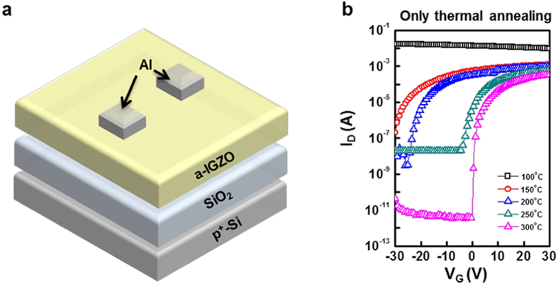
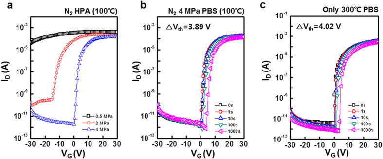
Figure 1b shows the transfer characteristics of the thermally activated a-IGZO TFTs, which were annealed for 1 hour at 100, 150, 200, 250 and 300 °C. The TFTs annealed at ≤250 °C did not exhibit satisfactory on/off current ratios for applications as switching devices (i.e. >106). Thus, the annealing temperature of sputter-processed a-IGZO TFTs should be at least 300 °C to activate the a-IGZO channel layer. The electrical characteristics of the thermally activated a-IGZO TFTs at 300 °C exhibited the following characteristics: μFE = 7.43 cm2/V.s, S.S = 0.39, the on/off current ratio = 1.10 × 10⁸, and the the threshold voltage (Vth ) = 2.08 V (Supplementary Table S1). Figure 2a shows the transfer characteristics of the HPA-activated a-IGZO TFTs annealed for 1 hour at 100 °C in N2 gas at pressures in the range from 0.5 to 4 MPa. The a-IGZO TFTs were activated with pressures of ≥2 MPa, and the transfer characteristics of devices activated at 4 MPa were superior to those at 2 MPa. Figure 2b,c show the results of PBS tests for the a-IGZO TFTs annealed in N2 at 4 MPa at 100 °C, and those annealed at 0 MPa and 300 °C. The positive Vth shift of the devices annealed in N2 at 4 MPa was 3.65 V, and that annealed at 0 MPa and 300 °C was 4.02 V. The PBS stability of the a-IGZO TFTs was also improved by annealing in N2. It has previously been shown that annealing in N2 gas improved the PBS stability of a-IGZO TFTs by reducing deep level defects in the channel layer12.
Figure 1.
(a) Schematic structure of fabricated a-IGZO TFTs (b) Transfer characteristics of a-IGZO TFTs with only thermal annealing.
Figure 2.
(a) Transfer characteristics of HPA activated a-IGZO TFTs varying N2 pressure at 100 °C, and PBS test results of HPA activated a-IGZO TFTs under (b) N2 4 MPa at 100 °C (c) 300 °C for 1000 s.
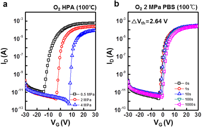
These results show that HPA in N2 improved the PBS stability of a-IGZO TFTs, while enabling the use of a low temperature of l00 °C to form the channel. However, the required pressure of N2 to activate the a-IGZO channel layer was relatively high. We also investigated the use of O2 gas during activation, exploiting both pressure and the metal–oxide construction (MOC) effect. Figure 3a shows the transfer characteristics of HPA-activated a-IGZO TFTs annealed in O2 at 100 °C and pressures of 0.5, 2 and 4 MPa. The transfer characteristics of the HPA-activated a-IGZO TFTs at 2 MPa were superior to those annealed at other pressures. The positive Vth shift of the a-IGZO TFTs annealed in O2 at 2 MPa was 2.64 V, as shown in Fig. 3b. The a-IGZO TFTs annealed in O2 at 2 MPa exhibited superior performance compared with the devices annealed in N2 at 4 MPa, despite the lower pressure (Supplementary Table S1). The electrical characteristics of the TFTs annealed in O2 at 2 MPa were as follows: μFE = 10.58 cm2/V.s, S.S = 0.45, the on/off current ratio = 1.34 × 10⁸, and Vth = 0.48 V.
Figure 3.
(a) Transfer characteristics of HPA activated a-IGZO TFTs varying O2 pressure at 100 °C (b) PBS test result of HPA activated a-IGZO TFTs under O2 2 MPa at 100 °C.
Discussion
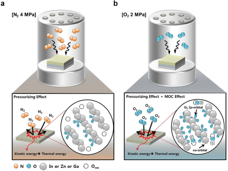
Figure 4a shows the activation mechanism of the a-IGZO TFTs annealed in N2 at 4 MPa and 100 °C, and Fig. 4b shows the activation mechanism annealed in O2 at 2 MPa and 100 °C. The activation of the a-IGZO channel layer in N2 gas can be described using the van der Waals equation, i.e.,
Figure 4.
The schematic mechanism of HPA activated a-IGZO channel layer under (a) N2 4 MPa and (b) O2 2 MPa at 100 °C.
 |
together with the ideal gas equations, i.e.,
 |
as well as the following thermodynamic relations:
 |
and
 |
where P, V, T, k, a, b, and R are applied to gas pressure, volume of HPA chamber, temperature, Boltzmann constant, intermolecular attractive force constant, volume of molecule, and gas constant, respectively. The van der Waals equation can be used to describe the activity of a gas in the HPA chamber13; however, we can use the ideal gas equation because the volume of the HPA chamber is much larger than nb (i.e., nb < V)14. The average kinetic energy of gas molecules can be described using equation (3). Pressure is proportional to temperature from equations (2) and (4) 15; thus, the kinetic energy of the gas molecules is equivalent to their thermal energy, and may serve as an energy source during thermal activation of the a-IGZO TFTs. We term this the “pressurizing effect”; when the pressurizing effect is applied with N2 gas, the a-IGZO channel layer can be activated by converting kinetic energy of the gas molecules to activation energy. The higher the pressure of N2 gas is applied, the greater the activation energy is supplied to activate a-IGZO channel layer. Therefore, the transfer characteristics of the HPA-activated TFTs annealed in N2 at 4 MPa were superior to those annealed at lower temperatures. We may expect that the collision frequency with N2 at 4 MPa will be double that in O2 at 2 MPa because it is proportional to the number of molecules16. Because the ratio of the molecular mass of N2 to O2 gas is 7:8, the average speed of the N2 molecules will be larger than that of the O2 gas molecules. Nonetheless, the O2 pressure required to activate the a-IGZO channel was half that with N2. This is attributed to the MOC effect as well as the pressurizing effect. The MOC effect indicates that the presence of the O2 gas during HPA aids the formation of direct overlapping ns orbitals among neighboring metals. Compared with HPA in N2 gas (without the MOC effect), more metal–oxygen bonds can be formed in an O2 environment. In addition, we could figure out that O2 gas improved PBS stability and had little effect on the on-current level of a-IGZO TFTs, as shown in Fig. 3b. It means that oxygen vacancies in deep levels are dominantly influenced by O2 gas15,17. Thus, we may expect that the density of oxygen vacancies (which act as electron trap sites) could be reduced by annealing in O2 gas.
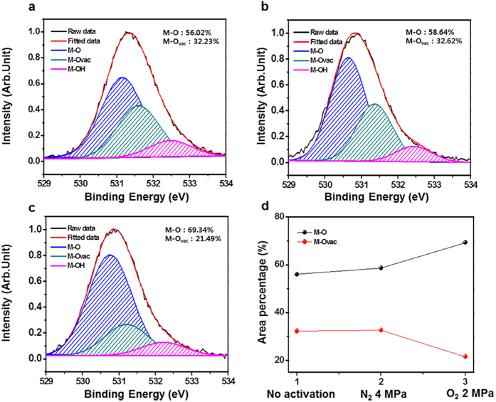
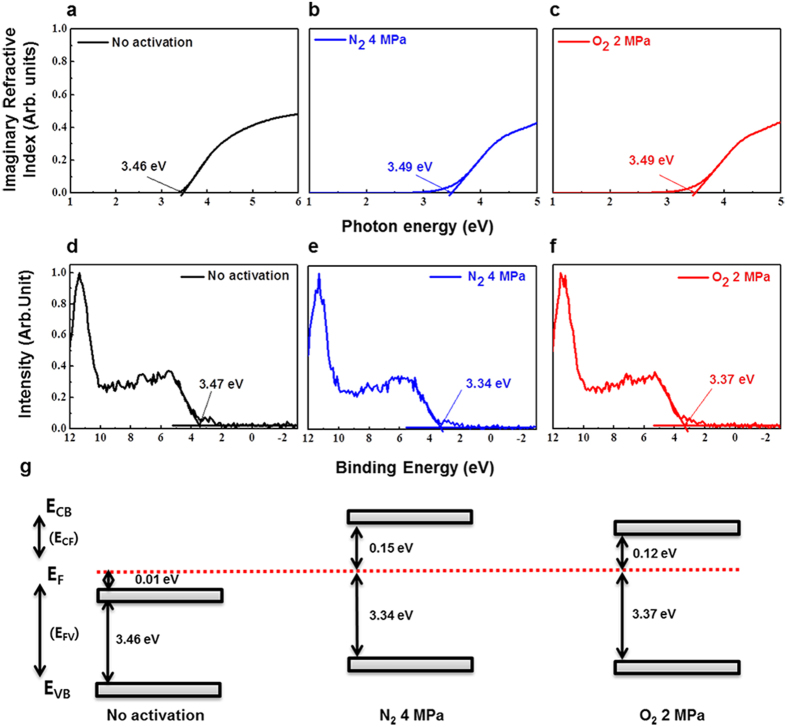
To investigate this mechanism of chemical composition change during HPA, we used X-ray photoelectron spectroscopy (XPS) to characterize the a-IGZO channel layers. Figure 5a–c show the O 1s peaks of the XPS spectra for the channel layers with no activation, with HPA in N2 at 4 MPa and 100 °C, and with HPA in O2 at 2 MPa and 100 °C. The ‘no activation’ indicates that a-IGZO channel layer is not influenced by thermal or pressuring process. There were three O 1 s peaks centered at 530.40 ± 0.1, 531.05 ± 0.1 and 532.35 ± 0.2 eV. These binding energy peaks indicate the metal–oxide (M-O), metal–oxygen vacancy (M-Ovac), and metal–hydrogen lattice (M-OH) bonds, respectively. The relative area of the M-O lattice, which forms conducting pathways for charge carriers, in HPA-activated a-IGZO channel layer formed in N2 at 4 MPa expanded slightly compared with the non-activated channel layer (M-O increased from 56.02% to 58.64%). The ratio of M-Ovac lattice in the non-activated channel layer was not significantly different from that in the channel annealed in N2 at 4 MPa (M-Ovac increased from 32.23% to 32.62%), as shown in Fig. 5a,b. The N2 gas had little effect on the formation of the a-IGZO channel layer because of its low reactivity. It follows that N2 activates the a-IGZO channel layer by forming M-O bonds due to the pressurizing effect. Comparing the HPA-activated a-IGZO channel layer annealed in O2 at 2 MPa (see Fig. 5c) with that annealed in N2 at 4 MPa (see Fig. 5b), the area of the M-O lattice was significantly larger for a-IGZO channel layer annealed in O2 2 MPa, whereas that of the M-Ovac lattice was significantly smaller (M-O increased from 58.64% to 69.34%, and M-Ovac decreased from 32.62% to 21.49%). We could figure out that the a-IGZO channel annealed in O2 at 2 MPa exhibited a higher ratio of M-O bonds compared with that annealed in N2 at 4 MPa. These results are summarized in Fig. 5d. It follows that more M-O bonds were formed by annealing in O2 at 2 MPa due to the pressurizing effect and the MOC effect. Furthermore, electron trapping is a dominant mechanism that explains the PBS stability of oxide TFTs18,19,20. The ionized Ovac defect related to M-Ovac leads to the PBS instabilities of oxide TFTs by forming trap sites for electrons. The a-IGZO channel layer annealed in O2 at 2 MPa exhibited a lower density of Ovac than that annealed in N2 at 4 MPa. This shows that HPA in O2 can activate the a-IGZO TFTs, as well as improve the PBS stability, using a lower pressure. Figure 6a–c show the imaginary part of the absorption coefficient from the spectroscopy ellipsometry (SE) spectra of a-IGZO channel layers with no activation, annealed in O2 at 2 MPa and 100 °C, and annealed in N2 at 4 MPa and 100 °C. The respective band gap energies were Eg = 3.46 eV, Eg = 3.49 eV and Eg = 3.49 eV. Figure 6d–f show the band offsets for each sample, including the Fermi energy EF and the valence band energy EVB, which were obtained from the XPS spectra in the vicinity of the valence band energy. Using these data, we calculated the valence band offsets, as well as the differences in EF and the conduction band energy ECB. We summarized the value of Eg, EVB − EF = EFV, and ECB − EF = ECF for each sample (Supplementary Table S2). Figure 6g shows the band alignments of the a-IGZO channels formed with the three conditions. With no activation, the a-IGZO channel layer was degenerate, as EF was located above ECB, and hence the channel layer was not semiconducting. The energy ECF of a-IGZO channel layer annealed in O2 at 2 MPa was lower than those annealed in N2 at 4 MPa. In general, the electron concentration decreases exponentially as ECF increases and the Hall mobility is proportional to the carrier concentration21,22. Furthermore, μFE is proportional to the Hall mobility in oxide semiconductors23,24,25. From these results, we may conclude that the μFE for the HPA-activated a-IGZO TFTs annealed in O2 at 2 MPa was larger than that for the devices annealed in N2 at 4 MPa. From the XPS and SE data, we may conclude that the sputter-processed a-IGZO TFTs should be activated for use as semiconductor devices; that the sputter-processed a-IGZO TFTs could be annealed in N2 at 4 MPa or O2 at 2 MPa and 100 °C; and that the electrical characteristics and PBS stability of the HPA-activated a-IGZO TFTs annealed in O2 at 2 MPa were superior to those annealed in N2 at 4 MPa, despite the lower pressure.
Figure 5.
The O 1 s peaks of XPS analysis in a-IGZO channel layer under different conditions (a) no activation, (b) N2 4 MPa at 100 °C, and (c) O2 2 MPa at 100 °C. (d) Area ratio of M-O and M-Ovac in each condition.
Figure 6.
(a–c) Imaginary part of SE spectra absorption coefficient, (d–f) XPS spectra near the valence band and (g) band alignment of a-IGZO channel layer under different conditions: no activation, O2 2 MPa at 100 °C, and N2 4 MPa at 100 °C.
We have investigated the effects of HPA as an energy source to activate the a-IGZO channel layers as well as a method to improve the PBS stability. Activated a-IGZO TFTs were formed by annealing for 1 hour at 100 °C in N2 at 4 MPa, and in O2 at 2 MPa. The a-IGZO TFTs annealed in O2 required lower pressure for activation, and exhibited superior electrical characteristics. Furthermore, we investigated the mechanisms of HPA activation; i.e., the pressurizing effect and the MOC effect. We fabricated a-IGZO TFTs with excellent electrical performances and PBS stability via HPA in O2 at 2 MPa and 100 °C. Furthermore, we suggest that this process is feasible for the low-temperature activation of AOS-TFTs based on various flexible substrates.
Methods
The a-IGZO TFTs were fabricated with inverted staggered structure. A SiO2 (1200 Å) layer was thermally oxidized on heavily boron-doped silicon (p+-Si) as a gate insulator. Then a-IGZO layer (40 nm) was deposited on the cleaned SiO2/p+-Si using radio-frequency (RF) magnetron sputtering at room temperature. The composition ratio of a-IGZO target was In2O3:Ga2O3:ZnO = 1:1:1. The RF power, operation pressure, and oxygen partial pressure ([O2]/[Ar + O2]) of sputtering process were fixed to 150 W, 5.0 × 10⁻³ Torr, and 0%, respectively. After a-IGZO channel was deposited on SiO2, the HPA was performed in different conditions: 100 °C under N2 (0.5, 2, and 4 MPa), and 100 °C under O2 gases (0.5, 2, and 4 MPa). The channel width and length were set to 1000 and 150 μm, respectively. Finally aluminum source/drain electrodes (200 nm) via shadow mask were deposited by thermal evaporation. Figure 1a shows the schematic structure of inverted staggered a-IGZO TFTs. Electrical characteristics of a-IGZO TFTs were measured by a HP 4156 C semiconductor parameter analyzer. To analyze the positive bias stability, PBS was conducted under VGS = 20 V and VDS = 10.1 V for 1000 s. The chemical bonding composition of a-IGZO channel layer was measured using X-ray photoelectron spectroscopy (XPS). Furthermore, we used XPS spectra near the valence band and spectroscopy ellipsometry (SE) to determine the valence band offset and the band gap energy of a-IGZO channel layer, respectively.
Additional Information
How to cite this article: Kim, W.-G. et al. High-pressure Gas Activation for Amorphous Indium-Gallium-Zinc-Oxide Thin-Film Transistors at 100 °C. Sci. Rep. 6, 23039; doi: 10.1038/srep23039 (2016).
Supplementary Material
Acknowledgments
This work was supported by Samsung Display and the National Research Foundation of Korea (NRF) grant funded by the Korea government (MSIP) (No. 2011-0028819).
Footnotes
Author Contributions W.G.K. designed the experimental process and wrote the main manuscript. Y.J.T. fabricated the device. B.D.A. measured the electrical characteristics of device. Y.J.T., B.D.A., T.S.J. and K.B.C. discussed the results and provided a theoretical advice for proceeding experiment. The project was guided by H.J.K.
References
- Hosono H. et al. Working hypothesis to explore novel wide band gap electrically conducting amorphous oxides and examples. J. Non-Cryst. Solids 198, 165–169 (1996). [Google Scholar]
- Nomura K. et al. Thin-film transistor fabricated in single-crystalline transparent oxide semiconductor. Science 300, 1269–1272 (2003). [DOI] [PubMed] [Google Scholar]
- Kim S. J. et al. Review of solution-processed oxide thin-film transistors. Jpn. J. Appl. Phys. 53, 02BA02 (2014). [Google Scholar]
- Nag M. et al. High performance a-IGZO thin-film transistors with mf-PVD SiO2 as an etch stop-layer. J. Inf. Disp. 22, 23–28 (2014) [Google Scholar]
- Ahn B. D. et al. A novel amorphous InGaZnO thin film transistor structure without source /drain layer deposition. Jpn. J. Appl. Phys. 48, 03B019 (2009). [Google Scholar]
- Stanley Williams R. Low energy Ar ion bombardment damage of Si, GaAs, and InP surfaces. Solid State Commun. 41, 153–156 (1982). [Google Scholar]
- Ji K. H. et al. Effect of high-pressure oxygen annealing on negative bias illumination stress-induced instability of InGaZnO thin film transistors. Appl. Phys. Lett. 98, 103509 (2011). [Google Scholar]
- Noh H. K. et al. Electronic structure of oxygen-vacancy defects in amorphous In-Ga-Zn-O semiconductors. Phys. Rev. B 84, 115205 (2011). [Google Scholar]
- Seo D. K. et al. Drastic improvement of oxide thermoelectric performance using thermal and plasma treatments of the InGaZnO thin films grown by sputtering. Acta Mater. 59, 6743–6750 (2011). [Google Scholar]
- Nomura K. et al. Room-temperature fabrication of transparent flexible thin-film transistors using amorphous oxide semiconductors. Nature 432, 488–492 (2004). [DOI] [PubMed] [Google Scholar]
- Kim M. J. et al. Low-temperature fabrication of high-performance metal oxide thin-film electronics via combustion processing. Nat. Mater. 10, 382–388 (2011). [DOI] [PubMed] [Google Scholar]
- Yoon S. H. et al. Study of nitrogen high-pressure annealing on InGaZnO thin-film transistors. ACS Appl. Mater. Interfaces 6, 13496–13501 (2014). [DOI] [PubMed] [Google Scholar]
- Tao J. et al. Accurate van der Waals coefficients from density functional theory. Proc. Natl. Acad. Sci. USA 109, 18–21 (2011). [DOI] [PMC free article] [PubMed] [Google Scholar]
- Kauzmann W. [Kinetic Theory of Gases ] [130–135] (W. A. Benjamin Inc., 1966). [Google Scholar]
- Ahn B. D. et al. Origin of electrical improvement of amorphous TaInZnO TFT by oxygen thermos-pressure-induced process. J. Phys. D-Appl. Phys. 47, 105104 (2014). [Google Scholar]
- Greiner M. et al. Emergence of a molecular Bose-Einstein condensate from a fermi gas. Nature 426, 537–540 (2003). [DOI] [PubMed] [Google Scholar]
- Park S. Y. et al. Improvement in the device performance of tin-doped indium oxide transistor by oxygen high pressure annealing at 150°C. Appl. Phys. Lett. 100, 162108 (2012). [Google Scholar]
- Kamiya T. et al. Electronic structure of oxygen deficient amorphous oxide semiconductor a-InGaZnO4-x: optical analyses and first-principle calculations. Phys. Status Solidi C 5, 3098–3100 (2008). [Google Scholar]
- Noh H. K. et al. Electronic structure of oxygen-vacancy defects in amorphous In-Ga-Zn-O semiconductors. Phys. Rev. B 84, 115205 (2011). [Google Scholar]
- Park J. H., Kim Y. G. et al. Simple method to enhance positive bias stress stability of In-Ga-Zn-O thin-film transistors using a vertically graded oxygen-vacancy active layer. ACS Appl. Mater. Interfaces 6, 21363–21368 (2014). [DOI] [PubMed] [Google Scholar]
- Avadhanulu M. N. & Kshirsagar P. G. A Textbook of Engineering Physics 8th edition (S. Chand & Company LTD, 2000). [Google Scholar]
- Takagi A. et al. Carrier transport and electronic structure in amorphous oxide semiconductor, a-InGaZnO4. Thin Solid Films 486, 38–41 (2005). [Google Scholar]
- Suzuki T. I. et al. Hall and field-effect mobilities of electrons accumulated at a lattice-matched ZnO/ScAlMgO4 heterointerface. Adv. Mater. 16, 1887–1890 (2004). [Google Scholar]
- Kim G. H. et al. Effect of indium composition ratio on solution-processed nanocrystalline InGaZnO thin film transistors. Appl. Phys. Lett. 94, 233501 (2009). [Google Scholar]
- Kim Y. H. et al. Effect of metallic composition on electrical properties of solution-processed indium-gallium-zinc-oxide thin-film transistors. IEEE Trans. Electron Devices 57, 1009–1014 (2010). [Google Scholar]
Associated Data
This section collects any data citations, data availability statements, or supplementary materials included in this article.


