

Abstract
A 30-μW wireless fast-scan cyclic voltammetry monitoring integrated circuit for ultra-wideband (UWB) transmission of dopamine release events in freely-behaving small animals is presented. On-chip integration of analog background subtraction and UWB telemetry yields a 32-fold increase in resolution versus standard Nyquist-rate conversion alone, near a four-fold decrease in the volume of uplink data versus single-bit, third-order, delta-sigma modulation, and more than a 20-fold reduction in transmit power versus narrowband transmission for low data rates. The 1.5-mm2 chip, which was fabricated in 65-nm CMOS technology, consists of a low-noise potentiostat frontend, a two-step analog-to-digital converter (ADC), and an impulse-radio UWB transmitter (TX). The duty-cycled frontend and ADC/UWB-TX blocks draw 4 μA and 15 μA from 3-V and 1.2-V supplies, respectively. The chip achieves an input-referred current noise of 92 pArms and an input current range of ±430 nA at a conversion rate of 10 kHz. The packaged device operates from a 3-V coin-cell battery, measures 4.7 × 1.9 cm2, weighs 4.3 g (including the battery and antenna), and can be carried by small animals. The system was validated by wirelessly recording flow-injection of dopamine with concentrations in the range of 250 nM to 1 μM with a carbon-fiber microelectrode (CFM) using 300-V/s FSCV.
Keywords: Wireless integrated circuit (IC), neurochemical monitoring, fast-scan cyclic voltammetry (FSCV), impulse radio, ultra-wideband (UWB) telemetry, flow-injection analysis, analog background subtraction, dopamine, carbon-fiber microelectrode
I. Introduction
DOPAMINE is a neurotransmitter that plays a fundamental role in motor control [1] and reward-seeking behaviors including drug addiction and eating disorders [2]. Fast-scan cyclic voltammetry (FSCV) has become the most widely used electrochemical method for studying the intricate relationship between brain dopamine release and behavior [3]. With its subsecond temporal resolution and high chemical selectivity, it is the preferred technique for monitoring rapid changes in dopamine concentration levels in ambulatory subjects during brain-behavior studies [4].
Recent technological advances have enabled miniaturized devices that can achieve stress-free, wireless FSCV monitoring of dopamine release in freely-moving small animals [5], [6]. The main drawback of these battery-operated systems is their limited power budget. Resolving wide-range neurochemical signals with high chemical and temporal resolution mandates high-precision conversions and high sampling rates, and thus, high wireless transmission data rates, which considerably decrease battery life. Long-term monitoring in complex, enriched environments is a promising research direction in behavioral neuroscience that can provide further insights into behaviors such as social interaction and reward-based learning [7], [8]. To enable these long-term behavioral studies, wireless FSCV systems must implement energy-efficient data acquisition and wireless transmission schemes that meet the stringent dynamic range requirements of FSCV with minimal power.
In FSCV, the electrode potential is scanned periodically with a triangular waveform, and the resulting current is measured. One drawback of the technique is the fact that the small (±10 nA) redox current indicating dopamine concentration is buried by the large (±500 nA) background current produced due to the charging of the double-layer capacitance of the electrode-electrolyte interface [4]. Recent wireless FSCV microsystems have overcome this limitation by using high-order delta-sigma (ΔΣ) modulation to acquire the full span of the background with reduced in-band quantization noise at the expense of increased wireless data transmission rates [9]–[11]. Since the background has been proven to be stable over several hundred scans [12], these systems waste a significant fraction of their limited power budget repeatedly resolving and transmitting the same background information over consecutive scans. In theory, these systems can achieve the same dynamic range at lower data rates by systematically removing the redundant background before transmission.
This paper reports an ultra-low-power wireless FSCV monitoring IC that directly extracts and transmits only the relevant background-subtracted redox current, i.e., the dopamine signal. The chip achieves a dynamic range that is still within the same order of magnitude as that of state-of-the-art wireless FSCV sensing microsystems albeit at a fraction of the power. Two key insights enable the improved performance. First, we introduce a novel analog-to-digital converter (ADC) architecture that leverages the fact that the background is a periodic signal with a known quantization error, to increase the dynamic range without noise shaping. The two-step cyclic ADC achieves an extended dynamic range by performing real-time analog and digital background subtraction on-chip. By removing the background before transmission, the data rate requirement of the transmitter (TX) is also reduced. Second, we make use of a duty-cycled impulse-radio ultra-wideband (IR-UWB) TX, with power directly proportional to the data rate, which takes advantage of the reduced data rate to achieve wireless transmission with minimal power consumption.
The remainder of this paper is organized as follows: Section II describes how analog background subtraction increases the dynamic range while decreasing the data rate. Section III introduces duty-cycled UWB telemetry as a low-power alternative for short-range, low-data-rate monitoring applications. Section IV presents the architecture of the wireless FSCV IC. Section V details the implementation of the key circuit blocks. Section VI reports detailed experimental measurement results. Section VII provides a noise analysis of the sensing interface.
II. Analog Background Subtraction
In 300-V/s FSCV at a carbon-fiber microelectrode (CFM), a periodic sequence of 10-ms triangle waveforms is applied to the electrode every T = 100 ms, as illustrated in Fig. 1. In the absence of dopamine, the total input current is equal to the background current. In the presence of dopamine, the total input current is the sum of the background current and a time-dependent dopamine signal. Because the background is stable immediately before and after dopamine release, it can be modeled as a periodic signal with period T, for which
| (1) |
Using (1) and assuming dopamine release occurs at k > 0, the input current xk collected on the kth scan is given by
| (2) |
where xda,k is the time-dependent dopamine signal on the kth scan. Conversion of xk using an N-bit ADC yields a quantized signal with a quantization error ϵk given by
| (3) |
where Q is the quantization operator, and ϵk has a quantization width Δ = R/2N, where R is the ADC’s full-scale range. Typically, numerical background subtraction in software is used to recover the dopamine signal. In this case, a copy of the background current acquired just before dopamine release (k = 0) is subtracted from the total current acquired during dopamine detection (k > 0). Thus, for k > 0, the output yk after numerical background subtraction can be written as
| (4) |
Applying (2) and (3) to (4) yields
| (5) |
where has a quantization width Δ′ given by
| (6) |
where xmax is the maximum amplitude of the input current xk, which also spans the full-scale range of the ADC. Equation (6) implies that accurate measurement of the very small dopamine signal requires a high-resolution N-bit ADC, where N is large. This is true even though many of the most significant bits are wasted on resolving the ever-present background signal that contains no new information. The need for a high-resolution ADC drives up the power budget for such systems.
Fig. 1.
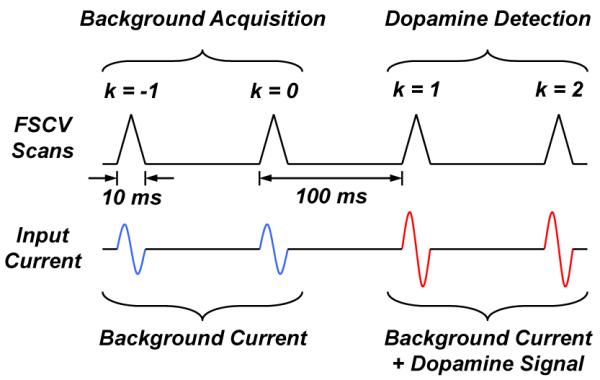
Dopamine detection using fast-scan cyclic voltammetry (FSCV) at a carbon-fiber microelectrode (CFM). For simplicity, a sinusoidal model with time-varying amplitude is used for the input current collected from the CFM.
Several techniques such as analog offset compensation [13], analog filtering [14], and analog background subtraction [15], have been proposed to reduce the magnitude of the background before conversion and thus increase the dynamic range of the ADC. Because the actual background is a nonlinear waveform, linear techniques such as offset compensation and filtering only achieve partial removal of the background. To circumvent this limitation, we present an analog background subtraction technique that performs coarse and fine quantization of the dopamine-free background signal over two consecutive FSCV scans. A key distinction of our work is that we subtract not just the periodic background signal but also its periodic quantization error. Subtraction of the latter signal is not possible in [15] due to the use of a high-resolution ADC with a quantization step size just above the uncorrelated noise of the system. Our implementation allows us to use a much lower resolution ADC and resolve a smaller number of significant bits by design, thus saving power in the TX. In our work, we restrict analog background subtraction to less than 40 seconds to minimize the distortion due to the drift of the background over extended timescales. This means that every 400 scans we repeat background acquisition and begin measuring the relative changes from that point in time. These can be recalibrated with respect to the initial current using the voltammograms measured just before the new background signal was acquired. As illustrated in Figs. 2 and 3, during the first scan (k = −1), a coarse copy of the background signal is digitized and stored in memory SRAM1 (solid blue line in Fig. 2a). During the second scan (k = 0), this coarse background copy is subtracted from a second background signal (dashed blue line in Fig. 2a) in the analog domain to recover the periodic quantization error of the background (Fig. 2b), which is quantized and stored in memory SRAM2. The sum of these two stored signals (coarse background + fine quantization error) is used to reconstruct a high-resolution background copy using a low-resolution ADC. This high-resolution copy is subsequently subtracted from the input signal during dopamine detection (k > 0) to recover the dopamine signal (Fig. 2c–2e). Thus, for k > 0, the output yk after analog background subtraction can be written as
| (7) |
where A is the gain of the rail-to-rail amplifier block in Fig. 3 needed to scale the background-subtracted residues (Figs. 2b and 2d) to span the ADC full-scale range. Choosing A = 2M, and applying (2) and (3) to (7) yields
| (8) |
where has a width Δ″ given by
| (9) |
Comparing (6) and (9) reveals analog background subtraction provides M additional bits of resolution for the same N-bit conversion. This increase in resolution compares favorably to that achieved through ΔΣ modulation, which roughly provides L+0.5 additional bits of resolution, where L is the modulator’s order, for each doubling of the oversampling ratio OSR. To achieve a dynamic range of N + M bits, where N + M is large, a single-bit ΔΣ modulator requires an OSR given by
| (10) |
Plugging N = 9 and M = 5 for the values used in this work and L = 3 for the third-order modulator in [10] into (10) yields an OSR of 32. This result indicates that even with the use of a high-order modulator, which increases design complexity and power consumption, a third-order ΔΣ ADC still requires 32× the sampling rate of the Nyquist ADC used in this work given the same dynamic range requirement. The reduced sampling rate in our work relaxes the wireless data rate requirement as follows. In a Nyquist ADC, the serialized unencoded data rate Rb is given by
| (11) |
where N is number of bits per sample, and fs is the Nyquist sampling rate. In an oversampling ΔΣ ADC, the undecimated unencoded data rate is given by
| (12) |
In [9]–[11], the unencoded data rate of the transmitter is equal to the undecimated data rate of the ΔΣ modulator because the decimation filter is implemented on the receiver side due to its complexity, area and power. Comparing (11) and (12) with N = 9 and OSR = 32 reveals the ADC in this work yields a 3.5× reduction in the wireless data transmission rate compared to the ADC in [10]. Assuming a wireless link with power directly proportional to the data rate, such as in a duty-cycled IR-UWB TX, this reduction also yields a 3.5× decrease in transmit power, the main component of the power budget in low-power wireless sensing systems.
Fig. 2.

Simplified diagram illustrating N-bit A/D conversion with analog background subtraction (a)-(e), versus ideal N + M-bit A/D conversion (f).
Fig. 3.

Simplified block diagram of the wireless FSCV monitoring microsystem with on-chip analog background subtraction and UWB telemetry.
III. UWB Telemetry
There has been considerable interest in high-data-rate UWB telemetry for biomedical applications requiring short-range, low-power wireless transmission. The inherent wide-spectrum (> 500 MHz) of UWB signals provides the bandwidth needed for multi-channel recording at high data rates [16], [17]. In fact, a high-data-rate IR-UWB-based transmission of in vitro FSCV measurements was recently demonstrated in [18]. UWB telemetry also offers numerous advantages for low-data-rate, energy-starved monitoring applications. The short duration of IR-UWB pulses (~2 ns) allows aggressive duty-cycling of the wireless link between consecutive pulses to achieve substantial power savings. In [19], we demonstrated duty-cycled IR-UWB radios consume considerably less power compared to narrowband systems at low data rates. This is because average power Pavg in a duty-cycled IR-UWB TX is linearly proportional to the data rate Rb, as given approximately by
| (13) |
where Eb is the energy efficiency (or energy per pulse), and P0 is a constant representing leakage and overhead power. Equation (13) suggests that for energy efficiencies in the order of 100 pJ/pulse, duty-cycled IR-UWB transmitters operating at a data rate of 100 kbps consume a few tens of microwatts, compared to the milliwatt power consumption of the narrowband systems in [9]–[11]. This orders-of-magnitude reduction in TX power associated with duty-cycled IR-UWB telemetry is critical to enable long-term brain-behavior studies.
IV. System Architecture
As noted in the introduction, the key insight of this paper is the combination of a transmitter topology for which the power consumption depends linearly upon the transmit data rate, and a data minimizing ADC that eliminates redundant background signals by design. Together, these two elements yield the low-power wireless FSCV microsystem depicted in Fig. 3, which operates as follows. A sequence of 300-V/s, 10-Hz FSCV scans generated off-chip is applied to a CFM via a low-noise potentiostat that also performs current-to-voltage (I/V) conversion. A 9-bit two-step cyclic Nyquist ADC performs analog background subtraction, as described in Section II, to directly resolve the dopamine signal during each 10-ms scan at 10-kS/s conversion rate. The core of the ADC is a switched-capacitor-based multiplying digital-to-analog (D/A) converter (MDAC), which achieves a high linearity by combining input sampling, D/A conversion, analog subtraction, and residue amplification into a single all-in-one block. As described in Section II, memories SRAM1 and SRAM2 are used to store the coarse and fine background copies during background acquisition. Both of the stored signals are subtracted from the input signal during dopamine detection to yield the background-subtracted dopamine signal. A stop bit is added to each 9-bit sampled data to form a 10-bit word that is then serialized at a data rate of 100 kbps. The serialized bit-stream is encoded at the IR-UWB TX into FCC-compliant pulses that are wirelessly transmitted via an off-chip surface mount UWB antenna to an external IR-UWB receiver (RX), previously demonstrated in [20], which achieves robust synchronization through a novel pulse-coupled oscillator scheme developed in [21].
V. Circuit Implementation
A. Low-Noise Potentiostat
Fig. 4 shows the schematic diagram of the low-noise potentiostat used in this work. The circuit is based on the current-mirror-based potentiostat described in [22] for a two-electrode electrochemical sensor. A two-electrode system is used in this work because the small currents involved in 300-V/s FSCV at a CFM produce a negligible ohmic drop that does not affect the reference electrode (RE) [23]. The potentiostat is a regulated common-gate (RCG) stage, also known as a regulated cascode amplifier (RCA) [24], consisting of a high-gain differential amplifier A(s) and transistor M1. The negative feedback loop in the RCG stage serves a three-fold purpose. First, it ensures that the potential of the working electrode (WE) is identical to the potential VSCAN. Second, it reduces the input resistance of M1 by the gain of the amplifier, ensuring that all of the input current iIN collected from the sensor is buffered to the drain of M1. Third, it increases the output resistance of M1 by the amplifier’s gain, ensuring that all of the buffered current is mirrored by an active current mirror onto resistor RP to produce a voltage VIN that is fed to the input of the ADC.
Fig. 4.
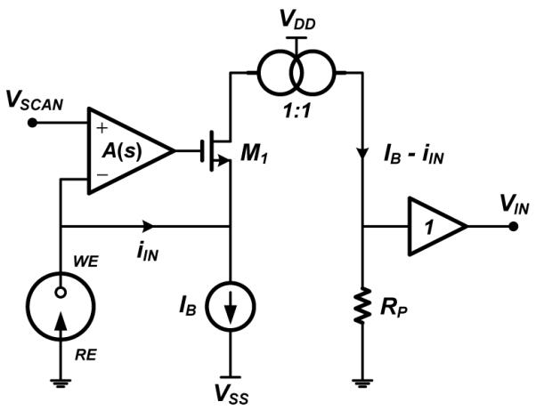
Schematic diagram of the current-mirror-based potentiostat, based on [22], designed for a two-electrode electrochemical sensor.
A transimpedance gain RP of 1 MΩ is used, followed by a unity-gain output buffer, which decreases the output resistance of the potentiostat. A single-stage, folded-cascode amplifier with a simulated open-loop gain of 50 dB and 3-dB bandwidth of 10 kHz is used for both the RCG feedback amplifier and the output buffer in the potentiostat. The RCG feedback amplifier draws 2 μA from a 3-V supply. The output buffer draws 10 μA during each 10-ms FSCV scan and is turned off for the 90-ms resting period between scans to save power. Thus, the duty-cycled buffer draws 1 μA from a 3-V supply. Duty cycling of the RCG amplifier is not possible as this block must stay active during the resting period to maintain the electrode potential at its resting value. A bias current IB is also used to allow the measurement of bidirectional redox currents [25].
B. Two-Step Cyclic ADC
As noted above, a key design element of this architecture is a two-step cyclic ADC, which is based upon a 1.2-V, 10-kS/s, 9-bit successive-approximation-register (SAR) ADC, depicted in Fig. 5, and two 100 × 9-bit, 6T-SRAM modules with their corresponding timing logic. As illustrated in Fig. 3, the core ADC samples the background signal and stores a copy in SRAM1. This quantized signal is then reproduced via a DAC and subtracted from a subsequent scan to form a residue. This signal is amplified to generate a periodic quantization error signal which is stored in SRAM2. This step is distinct from previous work by [15], and was first proposed by the authors in [26]. Together, these two signals form a high-fidelity background copy. The binary-weighted capacitor array of the SAR-ADC is laid out in a 1-D common-centroid geometry with a unit capacitance value of 62.5 fF for kT/C noise considerations as well as to mitigate offset and gain errors due to capacitor mismatch and charge injection.
Fig. 5.
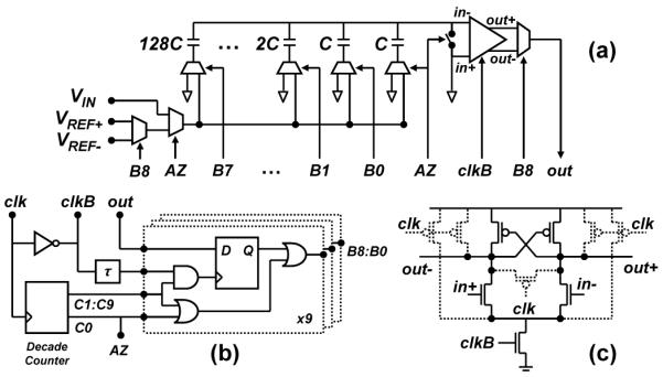
(a) Schematic diagram of the 9-bit successive approximation register (SAR) ADC with (b) its control logic and (c) dynamic latched-comparator.
Fig. 6 shows a circuit diagram of the 1.2-V, 10-kS/s, 9-bit, switched-capacitor MDAC block with offset cancellation. The MDAC uses an identical copy of the capacitor array in the SAR-ADC. A two-stage folded-cascode operational amplifier (op-amp) with simulated open-loop gain of 77 dB, unity-gain bandwidth of 3 MHz and phase margin of 65° is used as the residue amplifier. The op-amp draws 21 μA from a 1.2-V supply but is duty-cycled to draw an average current of 2 μA.
Fig. 6.
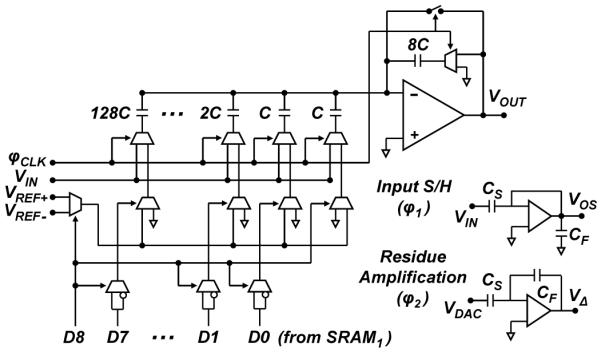
Schematic diagram of the switched-capacitor multiplying digital-to-analog converter (MDAC) circuit.
Reference voltages VREF+ and VREF− are set to 1.2 V and 0 V, respectively, to yield a full-scale range that spans the entire supply. The MDAC uses offset binary encoding to avoid bootstrapping and enable low-power operation from a 1.2-V supply. In this encoding scheme, the MSB (D8) of the data stored in SRAM1 simultaneously controls which reference gets selected and performs the necessary bit negation of the LSBs (D7–D0).
Fig. 7 shows the timing diagram of the core ADC. A hundred samples are acquired at a sampling rate of 10 kHz during each 10-ms FSCV scan. Each 100-μs conversion consists of a 10-μs input sample-and-hold (S/H) phase (ϕ1) and a 90-μs residue-amplification phase (ϕ2) to accommodate the op-amp settling times during each of the phases. During the input S/H phase, the capacitor array samples the input while the feedback capacitor samples the offset of the amplifier. During the second phase, the LSBs of the data stored in SRAM1 decide whether each capacitor in the array is connected to the MSB-selected reference or to mid-scale. The ratio between the sampling and feedback capacitances yields a residue amplification closed-loop gain of A = 32 in this phase.
Fig. 7.
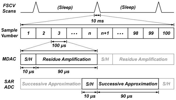
Timing diagram of the two-step cyclic core ADC.
C. IR-UWB Transmitter
The other critical design element to enable low power operation is the UWB transmitter. Fig. 8 (left) shows a schematic diagram of the duty-cycled IR-UWB TX implemented in this work. The topology is a modified version of the architecture in [27] with a unique digital tuning scheme. The TX block is comprised of an LC-tank voltage-controlled oscillator (VCO) and a class-C power amplifier (PA). An LC-tank oscillator is used over a ring oscillator for superior frequency stability and spectral purity. The design uses two 500-MHz sub-bands in the unlicensed 3.1–10.6 GHz UWB spectrum to transmit two types of pulses: synchronization (sync) pulses required for receiver synchronization, and data pulses, which are sent on separate 3.5 and 4.5 GHz channels, respectively, to improve interband isolation on the receiver side. On each rising and falling edge of the clock, a pulse generator outputs an enable signal that turns on the LC-tank oscillator for a brief duration to produce short wavelet pulses. As illustrated in Fig. 8 (right), sync pulses are sent on every positive edge of the clock, while data pulses are transmitted on the negative edge of the clock using an on-off-keying (OOK) encoding scheme. Triangular pulse-shaping is implemented with a simple charge-pump-based envelope generator to improve the spectral efficiency and to reduce the cross-talk between the two bands.
Fig. 8.

Schematic and timing diagrams of the duty-cycled IR-UWB transmitter with triangular pulse shaping and dual-band OOK pulse encoding schemes.
VI. Measurement Results
Fig. 9 shows a micrograph of the IC, which was fabricated in TSMC 65-nm CMOS process. The chip occupies 1.5 mm × 1.0 mm, including the bondpads. The measured average power consumption is 30 μW. The sensing interface, i.e. potentiostat and ADC, consumes 14.4 μW. The IR-UWB TX consumes 15.6 μW, which compares favorably against that of the IR-UWB TX reported in [18], which consumes ~19 μW from 1.2 V at 625 kHz and was implemented in a 90-nm CMOS node. The chip was packaged and assembled on a miniature PCB substrate with a few external components for ultra-low-power supply, bias, clock and triangle waveform generation. Fig. 10 illustrates the miniaturized wireless device, which draws a total average current of only 48 μA from a 3-V coin-cell battery. The triangle waveform generator was implemented off-chip for simplicity since the circuit required external RC integration and output filters in the first place. The block had a negligible contribution to the power budget of the miniaturized device due to the use of a 1.8-V, 700-nA COTS op-amp. The device measures 4.7 cm × 1.9 cm and weighs 4.3 g (including the battery and antenna), and thus can be carried by small animals. Table I summarizes the measured performance of the main circuit blocks of the fabricated chip. Table II compares the performance of the chip against that of recently published wireless FSCV monitoring microsystems.
Fig. 9.
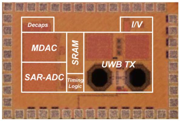
Micrograph of the 1.5 mm × 1.0 mm wireless FSCV monitoring IC.
Fig. 10.
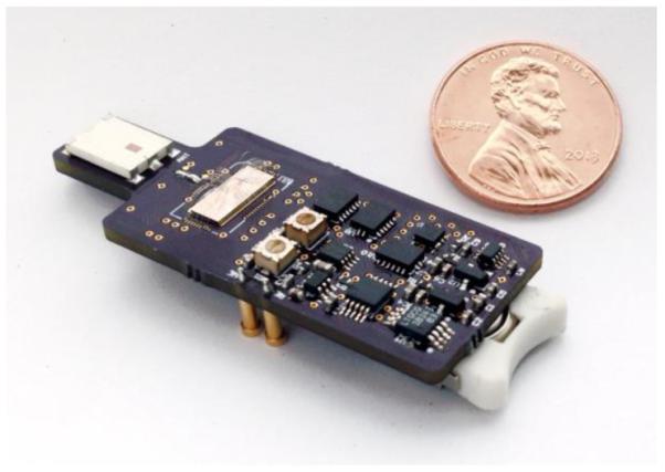
Miniaturized wireless device, which operates from a 3-V coin-cell battery, measures 4.7 cm × 1.9 cm, and weighs 4.3 g (with battery + antenna).
TABLE I.
Summary of Measured Performance
| Conversion Rate | 10 kS/s |
| Input Current Range | ±430 nA |
| Input-Referred RMS Noise | 92 pA (2-kHz BW) |
| Total Power Consumption | 30 μW |
| Power Supply | 1.2 V & 3.0 V (2.1 V, −0.9 V) |
| Total Chip Area | 1.5 mm × 1.0 mm |
| Communication Scheme | UWB @ 3.5 & 4.5 GHz |
| Unencoded Data Rate | 100 kbps |
| Technology | TSMC 65-nm CMOS |
TABLE II.
Performance Comparison of Wireless FSCV Microsystems
| This work | [9] | [10] | [11] | |
|---|---|---|---|---|
| No. Channels | 1 | 1 | 4 | 1 |
| ADC Scheme | Nyquist | 2nd−ΔΣ | 3rd−ΔΣ | 3rd−ΔΣ |
| TX Scheme | IR-UWB | FSK | FSK | FSK |
| TX Data Rate | Low | High | High | High |
| Carrier Freq. | 3.5-4.5 GHz | 433 MHz | 433 MHz | 433 MHz |
| Power Supply | 1.2, 3.0 V | ±1.3 V | ±1.25 V | −0.8, 1.7V |
| Sample Rate | 10 kHz | 10 kHz | 10 kHz | 10 kHz |
| Input Range | ±430 nA | ±430 nA | ±750 nA | ±950 nA |
| Input Noise1 | 92 pA | 132 pA | 57 pA | 55 pA |
| Bandwidth | 2 kHz | 5 kHz | 5 kHz | 5 kHz |
| Frontend Power | 14.4 μW | 57 μW | 76 μW | 9.3 μW |
| Transmit Power | 15.6 μW | ~1 mW | ~1 mW | ~0.4 mW |
| Total Power | 30 μW | ~1 mW | ~1 mW | ~0.4 mW |
| CMOS Node | 65 nm | 0.5 μm | 0.5 μm | 0.35 μm |
| Paradigm | In Vitro | In Vivo | In Vivo | In Vivo |
open input, ADC quantization noise included
A. Device Characterization
As described in Section II, the core ADC does not digitize absolute input currents but rather resolves directly small input current differences relative to an arbitrary baseline current. To test the static linearity of the potentiostat and the core ADC, the input current was swept linearly in the range of ±10 nA in steps of 50 pA relative to a DC offset baseline current using a Keithley 236 DC current source. Fig. 11 shows the measured output current for positive and negative baseline-subtracted input currents ranging from 50 pA to 10 nA. The distortion at ±10 nA was measured to be < 0.1% of the input range, and was found to be dominated by amplifier saturation. Thus, it could be accurately modeled with a simple hyperbolic tangent fit. A one-time calibration procedure using the inverse of this tanh fit was performed offline during post processing to further reduce the distortion for all input currents in the range of ±10 nA to < 0.01%. Fig. 12 (top) shows the measured ADC output spectrum for a 100-Hz ±10-nA sinusoidal input signal, from which ENOB values of 5.95 and 10.95 bits were calculated before and after analog background subtraction, respectively. As seen in Fig. 12 (bottom), the ADC exhibits minimal distortion with ∣INL∣ < 1 LSB.
Fig. 11.
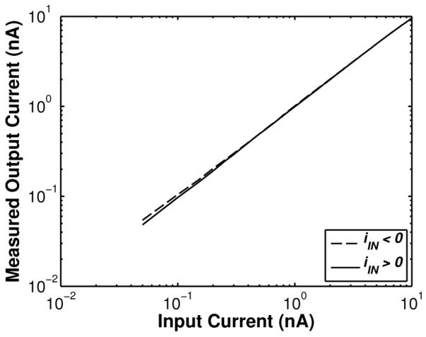
Measured static linearity of the potentiostat and A/D converter for positive and negative input currents in the range of 50 pA to 10 nA.
Fig. 12.
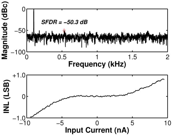
Measured dynamic (top) and static (bottom) ADC performance using a ±10-nA sinusoidal input and a slow-varying linear ramp, respectively.
B. Device Validation
For device validation with in vitro detection of dopamine, carbon fiber microelectrodes (CFMs) were fabricated as previously described in [15]. An individual carbon fiber with a 5-μm diameter was aspirated into a 1.8-mm glass capillary, which was heated and pulled on a micropipette puller. The exposed carbon fiber was cut to a length of ~150 μm under a microscope. Before use, the CFM was boiled in acetone and soaked in isopropanol purified with activated carbon for 15 minutes to remove surface impurities. The electrode was backfilled with a 150 mM KCl solution to promote electrical conduction between the CFM and a chlorinated silver wire inserted into the open end of the capillary. An Ag/AgCl electrode was used for the reference electrode. An in-house flow injection analysis apparatus was used to validate the chip. The CFM and reference electrode were positioned at the inlet of a flow cell reservoir connected to the outlet of a two-position, six-port sample injector. All experiments were done in a buffer solution mimicking physiological ion concentrations. The buffer solution contained 140 mM NaCl, 5 mM KCl, 2.5 mM CaCl2, 1 mM MgCl2, and 10 mM HEPES. NaOH was added to adjust the pH to 7.3. A 100 mM stock solution of dopamine, prepared on the same day of the experiments, was diluted in buffer solution to achieve concentration levels of 250 nM, 500 nM, and 1 μM. A syringe pump was used to introduce the buffer to the CFM at a flow rate of 1 mL/min. Before recording, consecutive 300-V/s, 10-Hz FSCV scans were applied to the CFM for 20 minutes to stabilize the electrode. The electrode voltage was swept from a resting value of −450 mV to a peak value of +1.05 V and back to its resting value in each scan. During recording, the sample injector was used to introduce a bolus of dopamine to the CFM. Background-subtracted dopamine signals were wirelessly recorded for all three concentrations. The CFM was kept immersed in the buffer solution during the entire recording session.
Fig. 13 illustrates a background-subtracted voltammogram (average of 10 scans) obtained from a wireless recording of flow injection of dopamine with a concentration level of 1 μM. The peak currents around +0.5 V and −0.2 V vs. Ag/AgCl correspond to dopamine oxidation and reduction, respectively. Fig. 14 illustrates the time course of the wirelessly-recorded dopamine oxidation current at +0.5 V (arrow in Fig. 13) after injection of a 250-μL, 15-second bolus of 1 μM dopamine solution at t = 0 seconds. The time course of the current reflects the dopamine concentration at the CFM. The slow decay at the end of dopamine injection is due to dopamine adsorption at the surface of the electrode, which decreases the response time. The strange dip observed around 15–20 seconds is an artifact that we believe was caused by small fluid perturbations at the inlet of the flow cell. Fig. 15 shows the calibration curve depicting measured dopamine oxidation current versus concentration. The data represent the mean of two independent wireless measurements for each concentration. In each trial, the mean is the average of 20 consecutive oxidation peaks starting at 8 seconds. The concentration dependence is linear with a sensitivity of 8.6 nA/μM. All eight (8) in vitro measurements were wirelessly transmitted and recorded at the receiver.
Fig. 13.
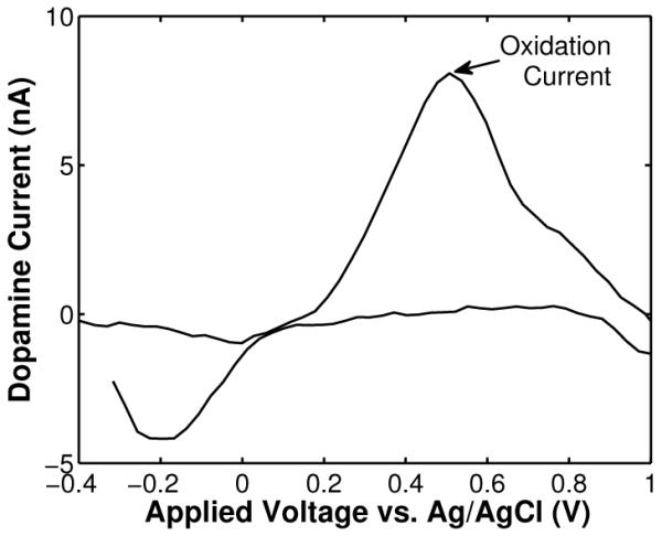
Background-subtracted cyclic voltammogram from a wireless recording of flow-injection of dopamine with a concentration level of 1 μM.
Fig. 14.
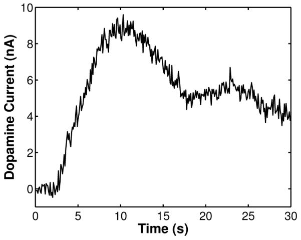
Time course of dopamine oxidation current from a wireless recording of flow-injection of a 250-μL bolus of 1-μM dopamine solution.
Fig. 15.
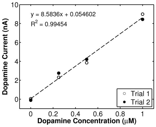
Calibration curve indicating oxidation current versus concentration, from wireless recordings of flow-injection of dopamine with concentration levels of 0 nM (buffer only), 250 nM, 500 nM, and 1 μM.
C. UWB Measurement Results
Fig. 16 illustrates the measured performance of the UWB transmitter. Fig. 16a depicts the measured output spectrum of the synchronization (sync) and data pulses at a pulse repetition rate of 100 kHz. Fig. 16b illustrates the measured transmitted time-domain sync pulse signal with triangular pulse shaping. Fig. 16c shows TX and RX timing signals indicating that the receiver can remain synchronized for at least up to 200 million cycles. Fig. 16d shows the position of the prototype TX and RX antennas used for the wireless FSCV experiments, which were carried out inside a grounded Faraday cage to minimize electrical interference. The antennas were separated by a distance of 0.6 m while still achieving a bit error rate (BER) better than 5×10⁻⁹.
Fig. 16.

UWB measurement results: (a) FCC-compliant spectrum of synchronization (sync) and OOK data pulses at a pulse repetition rate of 100 kHz, (b) time-domain sync pulse with triangle pulse shaping, (c) synchronized receiver (RX) over 200+ million cycles, and (d) antenna setup during FSCV monitoring.
VII. Noise Analysis
In this section we present a noise analysis of the major noise contributors of the wireless FSCV system. For simplicity, we ignore the ADC’s quantization noise as it is much smaller than the noise that appears at the input of the ADC during dopamine detection, which is predominantly input noise amplified by the potentiostat and MDAC stages. Fig. 17 shows a circuit diagram of the sensing interface, i.e., potentiostat and MDAC, interfaced to the CFM. The CFM is modeled with a simplified Randles circuit comprised of the solution resistance RS in series with the parallel combination of the charge-transfer resistance Rct and double-layer capacitance Cdl of the CFM. For the 150-μm CFM utilized in this work, values of RS = 100 kΩ, Rct = 100 MΩ, and Cdl = 1.5 nF were found to closely mimic the electrode’s response during flow injection analysis, respectively. The circuit in Fig. 17 has five dominant thermal noise sources: Vna1, Vna2, and Vna3, the equivalent input noise voltages of amplifiers OTA1, OTA2, and op-amp A3, respectively; and InRS and InM, the noise currents of the solution resistance and the current mirror transistors, respectively. Their spectral densities are given by
| (14a) |
| (14b) |
| (14c) |
| (14d) |
| (14e) |
where K is the Boltzmann constant, T is the absolute temperature, γ = 2/3 is the thermal noise coefficient for long-channel devices, gm1−3 and gm1−3,B are the transconductances of
| (15) |
| (16) |
the input and bias transistors of the amplifiers, respectively, and gm is the transconductance of the current mirror transistors. We neglect 1/f noise in (14a–14d) due to the use of long channel lengths, i.e., 40 μm. Neglecting channel-length modulation and body effect, and assuming all noise sources are uncorrelated, the output noise spectral density can be derived as (15), shown on the top of the page, where τz = RctCdl, τ1 = RSCdl, τ2 = RPCP, and τu is the inverse of the op-amp’s unity-gain bandwidth. In the derivation of (15), we have assumed OTA1 is a wideband single-stage amplifier with a time constant τa ⪡ τ1,2, and a high open-loop gain. Integrating (15) across 0 < f < ∞, as derived in [28], and dividing by yields the total input-referred noise current, given by (16). Applying (14) to (16), plugging design values and taking the square root yields an input noise current σn = 89 pArms in a 2-kHz bandwidth. This value is in excellent agreement with the measured value σn = 92 pArms, which is within the same order of magnitude as those reported in Table II. The last term in (16), which represents the reset noise of the MDAC op-amp, is the limiting factor degrading noise performance due to the small τu required to achieve a fast settling time of 10 μs during the input S/H phase (ϕ1). Reducing the op-amp’s unity-gain bandwidth is critical to improve the overall noise performance of the system. One way to achieve this goal is to redesign the MDAC block in a future design such that ϕ1 = ϕ2.
Fig. 17.
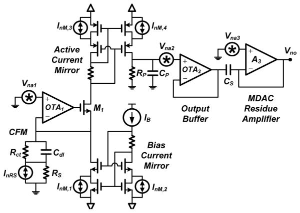
Schematic diagram illustrating the dominant noise sources in the sensing interface and the carbon-fiber microelectrode (CFM).
VIII. Conclusion
This paper reported an integrated wireless FSCV microsystem that combines analog background subtraction with UWB telemetry to achieve ultra-low-power, low-data-rate wireless transmission of high-precision FSCV measurements without loss of salient data. On-chip integration of these two techniques yielded a 32-fold increase in resolution versus standard Nyquist-rate conversion alone and near a four-fold decrease in the volume of uplink data versus single-bit, third-order, ΔΣ modulation, and more than a 20-fold reduction in transmit power versus narrowband transmission at reduced data rates. The microsystem was also validated with wirelessly-recorded flow-injection analysis experiments, and for the first time, IR-UWB telemetry in an experimental FSCV recording paradigm other than a single recording in saline [18] was demonstrated. A lightweight miniaturized device that can enable long-term monitoring studies in freely-behaving small animals was also reported. The device can operate from a single 3-V, 30-mAh coin cell battery for several weeks. To the best of the authors’ knowledge, the chip and miniaturized device presented in this work achieve the lowest power consumption among recently reported wireless FSCV sensing microsystems. Implementing the design in 65-nm technology offered a clear advantage in terms of power savings versus 0.35 μm designs. Since dynamic power scales according to P ∝ CV2f, it is evident that the reduced supply voltage played a major role in achieving the low power figures reported. Similarly, the reduced feature size allowed the integration of on-chip memory with minimal area and power. However, the reduced clock frequency due to use of Nyquist-based analog background subtraction over ΔΣ modulation was equally instrumental to the reduced power. A recent publication showed the overall power consumption can be reduced further, by an order of magnitude, by decreasing the scan repetition rate in FSCV from 10 Hz to 1 Hz [29]. Although this approach reduces the amount of data transmitted by a factor of 10×, it also reduces the total number of samples recorded by the same amount. Typically, in 10-Hz FSCV, data from 10 consecutive FSCV scans are averaged when producing the time course of dopamine. Lowering the repetition rate will similarly decrease the signal-to-noise ratio by a factor of . Finally, we note that ΔΣ modulation is, in fact, compatible with analog background subtraction, and that integration of both techniques into a single hybrid converter can further increase the overall dynamic range of either system.
Acknowledgment
The authors thank Joan S. Lenz for her excellent technical assistance and the TSMC University Shuttle Program for chip fabrication.
This work was supported in part by the National Science Foundation under Grant DGE-0654112 and the National Institutes of Health under Grant R01MH095046.
Biography

Carlos I. Dorta-Quiñones (S’07) received the B.S. degree in electrical engineering and computer science from Massachusetts Institute of Technology (MIT), Cambridge, MA, USA, in 2004, the M.S. degree in electrical engineering from Boston University, Boston, MA, USA, in 2007, and the Ph.D. degree in electrical and computer engineering from Cornell University, Ithaca, NY, USA, in 2014.
During his graduate studies, he held internships at IBM, Mitsubishi Electric Research Laboratories, and Freescale Semiconductor. He is currently with Cavium, Marlborough, MA, where he is working on the analysis and modeling of high-speed serial links. His research interests include analog, mixed-signal, and RF integrated circuit design.
Xiao Y. Wang (S’11) received the B.S. degree (with honors) in electrical engineering from the California Institute of Technology, Pasadena, CA, USA, in 2005, and the M.S. and Ph.D. degrees in electrical and computer engineering (with a minor in applied mathematics) from Cornell University, Ithaca, NY, USA, in 2010 and 2012, respectively.
He is currently with the Massachusetts Institute of Technology (MIT) Lincoln Laboratory, Lexington, MA, USA, where his research area is in equalization of receiver and ADC distortions through nonlinear system identification methods and baseband signal processing.

Rajeev K. Dokania received the B.Tech degree in electrical engineering from IIT Kharagpur, India, in 2003, and the M.S. and Ph.D. degrees in electrical and computer engineering from Cornell University, Ithaca, NY, USA, in 2008 and 2010, respectively.
He is currently with Intel Corporation, Hillsboro, OR. He has authored or co-authored more than 20 technical papers and patents. His research interests include low power radios, I/O circuit design, DFT/DFX, PM IC, optical interconnect, and hardware architecture.

Alycia Gailey received the B.S. degree in electrical engineering from the University of Massachusetts, Amherst, MA, USA, in 2006, and the M.S. and Ph.D. degrees in biomedical engineering from Cornell University, Ithaca, NY, USA, in 2009 and 2014.
She is currently a postdoctoral researcher at Arizona State University, Tempe, AZ, USA, where she is developing myoelectric-controlled hand prostheses. She is particularly interested in the link between robotics and neuro-motor control.

Manfred Lindau received the doctoral degree in physical chemistry from the Technical University of Berlin, Berlin, Germany, in 1983.
In 1988, he became Assistant Professor at the Free University of Berlin, Berlin, Germany. From 1992 through 1997, he was an Associate Member of the Max-Planck-Institute for Medical Research, Goettingen, Germany, and also taught biophysics at the University of Heidelberg, Heidelberg, Germany. He joined the faculty of Cornell University, Ithaca, NY, in 1997, where he is Professor of Applied and Engineering Physics and leads an interdisciplinary research group. He has developed biophysical techniques for cell and neurobiology including the first perforated patch recordings, improved cell-attached patch capacitance measurements, development of patch amperometry, and the first successful fabrication and application of surface-patterned amperometric electrode arrays. The central goal of his current research is to elucidate the mechanisms of exocytotic fusion and transmitter release. He is active as a consultant in the areas of biophysics, physiology, and cell biology. He is a Founding Member, Member of the Executive Committee and Program Coordinator of the Nanoscale Cell Biology Program at the Science and Technology Center for Nanobiotechnology at Cornell.
Dr. Lindau was elected as a Member of the Asian Institute of NanoBio-Science and Technology. In 2003 he received a Research Award from the Alexander von Humboldt Foundation, Germany, in recognition of his scientific achievements. He is a member of the Biophysical Society and the Society for Neuroscience.

Alyssa B. Apsel (S’94–A’02–M’03–SM’10) received the B.S. degree from Swarthmore College, Swarthmore, PA, USA, in 1995, and the Ph.D. degree from Johns Hopkins University, Baltimore, MD, USA, in 2002.
In 2002, she joined Cornell University, Ithaca, NY, USA, where she is currently an Associate Professor of electrical and computer engineering. She has authored or coauthored over 90 refereed publications in related fields of RF mixed-signal circuit design, interconnect design and planning, photonic integration with very large scale integration (VLSI), and process invariant circuit design techniques. She holds five patents with several patents pending. The focus of her research is on power-aware mixed-signal circuits and design for highly scaled CMOS and modern electronic systems.
Dr. Apsel has served as an associate editor for various journals, including the IEEE Transactions on Circuits and Systems—I: Regular Papers and IEEE Transactions on Circuits and Systems—II: Briefs. She was the chair of the Analog and Signal Processing Technical Committee of ISCAS 2011. She was the recipient of a Best Paper Award at ASYNC 2006. She had a MICRO “Top Picks” paper in 2006. She was the recipient of a college teaching award in 2007 and the National Science Foundation (NSF) CAREER Award in 2004. She was selected by Technology Review Magazine as one of the Top Young Innovators in 2004.
Contributor Information
Carlos I. Dorta-Quiñones, Cornell University, Ithaca, NY 14853 USA. He is now with Cavium, Marlborough, MA 01752 USA. (carlos.dorta@cavium.com).
Xiao Y. Wang, Cornell University, Ithaca, NY 14853 USA. He is now with MIT Lincoln Laboratory, Lexington, MA 02420 USA (xiao.wang@ll.mit.edu).
Rajeev K. Dokania, Cornell University, Ithaca, NY 14853 USA. He is now with Intel Corporation, Hillsboro, OR 97124 USA (rajeev.k.dokania@intel.com).
Alycia Gailey, Cornell University, Ithaca, NY 14853 USA. She is now with the School of Biological and Health Systems Engineering in Arizona State University, Tempe, AZ 85287 USA (alycia.gailey@asu.edu)..
Manfred Lindau, School of Applied and Engineering Physics, Cornell University, Ithaca, NY 14853 USA (ml95@cornell.edu)..
Alyssa B. Apsel, School of Electrical and Computer Engineering, Cornell University, Ithaca, NY 14853 USA (aba25@cornell.edu)..
References
- [1].Graybiel AM, Aosaki T, Flaherty AW, Kimura M. The basal ganglia and adaptive motor control. Science. 1994 Sep.265(no. 5180):1826–1831. doi: 10.1126/science.8091209. [DOI] [PubMed] [Google Scholar]
- [2].Baik JH. Dopamine signaling in reward-related behaviors. Front. Neural Circuits. 2013;7(no. 152):1–16. doi: 10.3389/fncir.2013.00152. [DOI] [PMC free article] [PubMed] [Google Scholar]
- [3].Garris PA, Ensman R, Poehlman J, Alexander A, Langley PE, Sandberg SG, Greco PG, Wightman RM, Rebec GV. Wireless transmission of fast-scan cyclic voltammetry at a carbon-fiber microelectrode: proof of principle. J. Neurosci. Meth. 2004;140(no. 1-2):103–115. doi: 10.1016/j.jneumeth.2004.04.043. [DOI] [PubMed] [Google Scholar]
- [4].Robinson DL, Venton BJ, Heien MLAV, Wightman RM. Detecting subsecond dopamine release with fast-scan cyclic voltammetry in vivo. Clin. Chem. 2003;49(no. 10):1763–1773. doi: 10.1373/49.10.1763. [DOI] [PubMed] [Google Scholar]
- [5].Roham M, Covey DP, Daberkow DP, Ramsson ES, Howard CD, Garris PA, Mohseni P. A miniaturized device for wireless FSCV monitoring of dopamine in an ambulatory subject. Proc. IEEE EMBS 32nd Annu. Int. Conf.; Aug. 2010; pp. 5322–5325. [DOI] [PubMed] [Google Scholar]
- [6].Kimble CJ, Johnson DM, Winter BA, Whitlock SV, Kressin KR, Horne AE, Robinson JC, Bledsoe JM, Tye SJ, Chang SY, Agnesi F, Griessenauer CJ, Covey D, Shon YM, Bennet KE, Garris PA, Lee KH. Wireless instantaneous neuro-transmitter concentration sensing system (WINCS) for intraoperative neurochemical monitoring. Proc. IEEE EMBS 31st Annu. Int. Conf.; Sep. 2009; pp. 4856–4859. [DOI] [PMC free article] [PubMed] [Google Scholar]
- [7].Garris PA, Greco PG, Sandberg SG, Howes G, Pongmaytegul S, Heidenreich BA, Casto JM, Ensman R, Poehlman J, Alexander A, Rebec GV. Electrochemical Methods for Neuroscience. CRC Press; Dec. 2006. In vivo voltammetry with telemetry; pp. 233–260. [Google Scholar]
- [8].Covey DP, Bennet KE, Blaha CD, Mohseni P, Lee KH, Garris PA. Integrated Microsystems. CRC Press; Oct. 2011. Technological evolution of wireless neurochemical sensing with fast-scan cyclic voltammetry; pp. 147–164. [Google Scholar]
- [9].Roham M, Daberkow DP, Ramsson ES, Covey DP, Pakdeerona-chit S, Garris PA, Mohseni P. A wireless IC for wide-range neurochemical monitoring using amperometry and fast-scan cyclic voltammetry. IEEE Trans. Biomed. Circuits Syst. 2008 Mar.2(no. 1):3–9. doi: 10.1109/TBCAS.2008.918282. [DOI] [PubMed] [Google Scholar]
- [10].Roham M, Covey DP, Daberkow DP, Ramsson ES, Howard CD, Heidenreich BA, Garris PA, Mohseni P. A wireless IC for time-share chemical and electrical neural recording. IEEE J. Solid-State Circuits. 2009 Dec.44(no. 12):3645–3658. [Google Scholar]
- [11].Bozorgzadeh B, Covey DP, Howard CD, Garris PA, Mohseni P. A neurochemical pattern generator SoC with switched-electrode management for single-chip electrical stimulation and 9.3 μW, 78 pArms, 400 V/s FSCV sensing. IEEE J. Solid-State Circuits. 2014 Apr.49(no. 4):881–895. [Google Scholar]
- [12].Hayes MA, Kristensen EW, Kuhr WG. Background-subtraction of fast-scan cyclic staircase voltammetry at protein-modified carbon-fiber electrodes. Biosens. Bioelectron. 1998;13(no. 12):1297–1305. doi: 10.1016/s0956-5663(98)00093-1. [DOI] [PubMed] [Google Scholar]
- [13].Howell JO, Kuhr WG, Ensman RE, Wightman RM. Background subtraction for rapid scan voltammetry. J. Electroanal. Chem. 1986;209(no. 1):77–90. [Google Scholar]
- [14].Cahill PS, Walker QD, Finnegan JM, Mickelson GE, Travis ER, Wightman RM. Microelectrodes for the measurement of catecholamines in biological systems. Anal. Chem. 1996;68(no. 18):3180–3186. doi: 10.1021/ac960347d. [DOI] [PubMed] [Google Scholar]
- [15].Hermans A, Keithley RB, Kita JM, Sombers LA, Wightman RM. Dopamine detection with fast-scan cyclic voltammetry used with analog background subtraction. Anal. Chem. 2008;80(no. 11):4040–4048. doi: 10.1021/ac800108j. [DOI] [PubMed] [Google Scholar]
- [16].Chae MS, Yang Z, Yuce MR, Hoang L, Liu W. A 128-channel 6 mW wireless neural recording IC with spike feature extraction and UWB transmitter. IEEE Trans. Neural Syst. Rehab. Eng. 2009 Aug.17(no. 4):312–321. doi: 10.1109/TNSRE.2009.2021607. [DOI] [PubMed] [Google Scholar]
- [17].Jafari HM, Abdelhalim K, Soleymani L, Sargent EH, Kelley SO, Genov R. Nanostructured CMOS wireless ultra-wideband label-free PCR-free DNA analysis SoC. IEEE J. Solid-State Circuits. 2014 May;49(no. 5):1223–1241. [Google Scholar]
- [18].Ebrazeh A, Mohseni P. 30 pJ/b, 67 Mbps, centimeter-to-meter range data telemetry with an IR-UWB wireless link. IEEE Trans. Biomed. Circuits Syst. 2014;PP(no. 99):1–1. doi: 10.1109/TBCAS.2014.2328492. [DOI] [PubMed] [Google Scholar]
- [19].Dokania RK, Wang XY, Tallur SG, Apsel AB. A low power impulse radio design for body-area-networks. IEEE Trans. Circuits Syst. I—Reg. Papers. 2011 Jul.58(no. 7):1458–1469. [Google Scholar]
- [20].Wang XY, Dokania RK, Apsel AB. A crystal-less self-synchronized bit-level duty-cycled IR-UWB transceiver system. IEEE Trans. Circuits Syst. I—Reg. Papers. 2013 Sep.60(no. 9):2488–2501. [Google Scholar]
- [21].Wang XY, Dokania RK, Apsel A. PCO-based synchronization for cognitive duty-cycled impulse radio sensor networks. IEEE J. Sensors. 2011 Mar.11(no. 3):555–564. [Google Scholar]
- [22].Ahmadi MM, Jullien GA. Current-mirror-based potentiostats for three-electrode amperometric electrochemical sensors. IEEE Trans. Circuits Syst. I—Reg. Papers. 2009 Jul.56(no. 7):1339–1348. [Google Scholar]
- [23].Murari K, Stanacevic M, Cauwenberghs G, Thakor NV. Integrated potentiostat for neurotransmitter sensing. 2005 Nov-Dec;24(no. 6):23–29. doi: 10.1109/memb.2005.1549726. [DOI] [PubMed] [Google Scholar]
- [24].Ayers S, Gillis KD, Lindau M, Minch BA. Design of a CMOS potentiostat circuit for electrochemical detector arrays. IEEE Trans. Circuits Syst. I—Reg. Papers. 2007 Apr.54(no. 4):736–744. doi: 10.1109/TCSI.2006.888777. [DOI] [PMC free article] [PubMed] [Google Scholar]
- [25].Genov R, Stanacevic M, Naware M, Cauwenberghs G, Thakor NV. 16-channel integrated potentiostat for distributed neurochemical sensing. IEEE Trans. Circuits Syst. I—Reg. Papers. 2006 Nov.53(no. 11):2371–2376. [Google Scholar]
- [26].Dorta-Quinones CI, Dokania RK, Apsel AB. Extending the dynamic range of implantable real-time neurochemical monitoring systems. 2011 Proc. IEEE Int. Symp. Circ. Syst. (ISCAS); May 2011.pp. 2353–2356. [Google Scholar]
- [27].Dokania R, Wang X, Tallur S, Dorta-Quinones C, Apsel A. An ultralow-power dual-band UWB impulse radio. IEEE Trans. Circuits Syst. II—Exp. Briefs. 2010 Jul.57(no. 7):541–545. [Google Scholar]
- [28].Oliveira LB, Leitao CM, Silva MM. Noise performance of a regulated cascode transimpedance amplifier for radiation detectors. IEEE Trans. Circuits Syst. I—Reg. Papers. 2012 Sep.59(no. 9):1841–1848. [Google Scholar]
- [29].Amos AN, Roberts JG, Lingjiao Q, Sombers LA, McCarty GS. Reducing the sampling rate of biochemical measurements using fast-scan cyclic voltammetry for in vivo applications. IEEE J. Sensors. 2014 Sep.14(no. 9):2975–2980. [Google Scholar]