Abstract
This paper presents the design, implementation, and performance of Rensselaer’s third-generation Adaptive Current Tomograph, ACT3. This system uses 32 current sources and 32 phase-sensitive voltmeters to make a 32-electrode system that is capable of applying arbitrary spatial patterns of current. The instrumentation provides 16 b precision on both the current values and the real and reactive voltage readings and can collect the data for a single image in 133 ms. Additionally, the instrument is able to automatically calibrate its voltmeters and current sources and adjust the current source output impedance under computer control. The major system components are discussed in detail and performance results are given. Images obtained using stationary agar targets and a moving pendulum in a phantom as well as in vivo resistivity profiles showing human respiration are shown.
I. Introduction
The goal of impedance imaging [2], [1], [9], [14] is to form estimates of the electrical impedance Z (p) at points p inside an object B. This impedance is, in general, a complex quantity, comprised of a real, or resistive, component and an imaginary, or reactive, component. The information for computing the estimate is derived from measurements of voltage made at the surface S of the object which arise as a result of the application of electric currents to S. The electric currents are typically sinusoidal at audio or higher frequency, and have maximum magnitudes on the order of 1 mA. In practice, data are collected on a finite number of electrodes, comprising an electrode array, attached to S. These voltage and current data form the input to a reconstruction algorithm, which computes the impedance distribution Z (p).
This paper discusses the design, implementation, and performance of Rensselaer’s third-generation Adaptive Current Tomograph, ACT3. The design goal for the resolution of ACT3’s phase sensitive voltmeters is one part in 216, or 16 b, for both the real and reactive voltage components. This is equivalent to a signal-to-noise ratio (SNR) of 104 dB for a full scale sinusoidal voltage input. In order to attain this high SNR, microprocessor-implemented discrete- time demodulators are used in place of traditional analog voltmeter techniques. Furthermore, in order to maintain a 16 b resolution throughout the system, the magnitudes of the currents output to the electrodes are specified to a similar resolution, and the interchannel phase coherence and phase linearity are strictly maintained. A high voltmeter resolution is of little value if the current source output impedance is not sufficiently large since a finite output impedance provides a path by which current output from the current source is shunted away from the electrode. It has been shown [8] that an output impedance of at least 64 MΩ is required, assuming a load impedance of 0–1 kΩ, to maintain 16 b accuracy. Maintaining an output impedance of this magnitude requires some sort of trimming arrangement for each current source. ACT3, a 32-electrode system, requires 32 independent current sources for the application of arbitrary current patterns. Such a large number of electrodes would require frequent, tedious manual adjustments to compensate for component variations with time and temperature. Therefore, ACT3 makes use of an automatic trimming procedure which uses a set of digitally programmable potentiometers to adjust the current source output impedances under computer control. Additionally, ACT3 provides the necessary hardware and software to automatically calibrate the voltmeters and current sources.
ACT3 acquires in 4.3 ms the voltages on all 32 electrodes that result from the application of one spatially distributed current pattern. Since a total of 31 current patterns are required for one resistivity image, the image acquisition rate of the ACT3 instrument is about 7.5 images/s with a voltmeter SNR of 104 dB. This acquisition rate can be increased, at the cost of reducing the voltmeter SNR, up to a maximum of about 480 images/s, at which the voltmeter SNR is reduced to 86 dB.
In anticipation of clinical trials, ACT3 provides several levels of patient protection. Safety features of ACT3 include optical isolation of all data communication signals, transformer isolation from the ac mains, and a novel ground current-monitoring system [7] which shunts all current away from the electrodes in the event of a system malfunction. The peak current applied to an electrode is a 0.5 mA, 30 kHz sinusoid. This ensures that the induced potential on the heart is significantly below the levels expected to induce fibrillation. A final safety feature of ACT3 is the gating of the output currents applied to the electrodes. That is, until the amplitude controls for all 32 output currents have been established internal to ACT3, currents are not applied to the electrodes. This results in a nearly instantaneous application of the 32 currents which together satisfy the conservation of charge constraint. ACT3 employs a 33rd ground electrode to serve as a voltage measurement reference; without this gating of the output current, a nonzero current would exist in this reference electrode until all 32 currents have been established on the electrodes at which the voltages are measured.
This paper first discusses the design of ACT3, and then presents data, in the form of quantitative results for system components and images, which illustrate the performance of the system.
II. ACT3 Design
ACT3 has been designed to implement as many functions as possible in digital, rather than analog, hardware. However, given the nature of an EIT instrument, several functions arc necessarily implemented in analog hardware. Details of the design and implementation of the main components are provided in the following sections.
A. Phase-Sensitive Voltmeter
The sinusoidal voltage appearing on an electrode is assumed to be of the form
where q (t) represents the presence of measurement noise. A major component in the impedance imaging system is the phase-sensitive voltmeter, which measures the real (Vr) and quadrature (Vq) voltages1 which are produced on the electrodes. A conventional approach to computing these voltage measurements is the continuous-time quadrature demodulator shown in Fig. 1. The structure in Fig. 1 consists of a pair of matched filters which, in principle, maximize the signal-to-noise ratio of the estimates at the sampling instant T. Analog multipliers are typically used in the hardware implementation of this voltmeter, but tend to suffer from limited dynamic range and relatively high noise levels. In addition, analog multipliers tend to exhibit nonlinearities on the order of 0.1% and direct signal feedthrough from input to output on the order of −60 dB. The analog integrators also introduce measurement error, as they are very sensitive to the dc offsets that are likely to be introduced by other analog components in the system. That these dc offsets vary with time and temperature further complicates matters. These nonidealities together serve to degrade the voltmeter SNR.
Fig. 1.
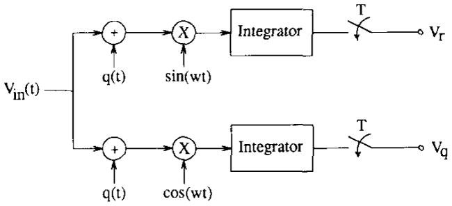
A continuous-time quadrature demodulator.
Due to the present availability of low-cost, high-speed digital signal processors (DSP’s) and the inherent limitations of the analog implementation, it is attractive to implement the demodulator in digital, rather than analog, hardware. Then, samples of the sin ωt and cos ωt demodulator signals can be computed analytically and stored in DSP memory, typically to at least 16 b of precision, and used to perform the quadrature demodulation. Denoting the sampled electrode voltage as Velec(i), the real and quadrature voltage estimates are given by
| (1) |
| (2) |
where N is the total number of samples in the observation interval. The multiplication and accumulation functions are performed digitally to great precision. Therefore, multiplier noise, which is a dominant noise source in the continuous-time implementation, is insignificant in the discrete-time implementation. Sampling noise can be reduced by employing a digital oscillator to generate a sinusoid with a high degree of magnitude and phase stability, and by choosing an analog-to-digital converter (ADC) with a very small sampling aperture uncertainty, such as Analog Devices’ 12 b AD678. This ADC has a resolution of 12 b and includes an on-chip sample-and- hold circuit.
I) Digital Voltmeter Signal-to-Noise Ratio
Consider for now the real channel of the voltmeter, defined by (1). Assuming that the noise sequence {q(i)} represents the quantization error introduced by the voltage sampling process,2 then the SNR of this channel is defined to be the ratio of the mean-squared value of the voltmeter output assuming no quantization noise and the mean-squared value of the voltmeter error due to quantization noise. Denoting the input to a ν bit uniform ADC as x(n) and the quantized output as x̃(n, ν), the mean-squared value of the quantization error, defined as eq(x; n, ν) ≡ x(n) − x̃(n, ν), is given by [6]
| (3) |
where (FS) is the full scale input range of the quantizer. The SNR of the real channel, then, is
| (4) |
If the noiseless, sampled input is taken to be
| (5) |
then (4) can be simplified [4] to produce
| (6) |
where it is assumed that the quantization noise is uncorrelated. Similarly, for the quadrature voltmeter channel,
| (7) |
Notice from (6) and (7) that for fixed N and ν, the SNR is maximized for M = FS and ϕ = 0° and ϕ = 90°, respectively. Therefore, N is chosen such that this maximum voltmeter SNR achieves a specified value. To achieve a maximum SNR of Γ dB requires, from (6) or (7), that N satisfy
| (8) |
A Γ of 104 dB by (8) requires that N ≥ 256 samples assuming an ADC resolution of 12 b. ACT3’s voltmeter uses N = 640 to allow overhead for SNR degradation caused by analog circuit noise and ADC sampling jitter.
Since the filter length N appears linearly in the quantities within square brackets in (6) and (7), every quadrupling of N results in a 6.02 dB increase in the SNR. This defines the tradeoff between the image acquisition rate and the SNR of the voltage estimates: reducing the value of N by a factor of 4δ allows the image acquisition rate to increase by a factor of 4δ while the SNR decreases by 6.02 × δ dB.
2) Nonuniform Sampling
One way to acquire the voltmeter input samples in (1) and (2) is to collect N uniformly spaced samples during one cycle of the sinusoid. However, for a sinusoid of 30 kHz and a filter length of 256 samples, the implementation of the discrete demodulator would require a sampling period of about 135 ns, which is unrealistic for low-cost 12 b ADC’s. Furthermore, it is not possible to achieve the same SNR improvement by acquiring R uniformly spaced samples, where R < N, and then averaging over N/R cycles for a total of N samples since this violates the assumption that the quantization noise sequence is uncorrelated. In fact, this would impose an R-periodic correlation on the sequence {q(j)} .The effect of averaging over the N/R cycles would therefore not improve voltmeter SNR beyond the theoretical limit obtainable by averaging R samples over one cycle. Of course, this assumes that the only noise source contributing to SNR degradation is quantization noise; averaging over several cycles would be useful in reducing the contribution from other uncorrelated noise sources.
A method of obtaining the voltmeter input samples which does not impose this R-periodicity upon the quantization sequence while allowing the use of available 12 b ADC’s is that of nonuniform sampling. R uniformly spaced samples are acquired during one cycle of a sinusoid of frequency ω0 rad/s for a total of S cycles. Unlike the uniform case outlined above, though, these R samples are delayed in time by 2π/ω0RS seconds cycle to cycle. Thus, a total of N ≡ R × S samples are acquired that, in effect, uniformly span one cycle of the sinusoid.
With uniform sampling, the voltmeter has a sin x/x frequency response [4] for frequencies near ω0. In order to assess the frequency response and bandwidth of the real and quadrature voltmeters defined by (1) and (2), a noise-free sinusoid of frequency α relative to the demodulator signal is applied to the input, and the output as a function of α is computed, this analysis is performed in [4], and the result for R = 5 and S = 128—the values used in ACT3—for a total of N = 640 samples is shown in Fig. 2. The full-width half-maximum (FWHM) bandwidth is found from the figure to be 122.4 Hz.
Fig. 2.
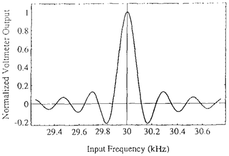
Frequency response of the real channel with R = 5. S = 128, and ϕ = 0—The half-power bandwidth is 100 Hz.
B. Analog Electronics
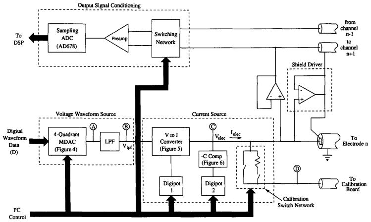
Fig. 3 is a block diagram of one analog board within the ACT3 instrument. Each analog board contains the analog hardware required for one electrode. The analog circuits have been divided into four functional units, two of which—the voltage waveform source and the current source—will be described below.
Fig. 3.
Block diagram of the analog circuits for one channel, showing the waveform source, current source, shield driver, and output signal conditioner.
1) Voltage Waveform Source [5]
In order to maintain a strict interchannel phase coherence, it is necessary that all channels derive the current to be applied to the electrode from a common, high-quality signal source. Digital sinusoid synthesis provides a practical means of establishing a highly phase- and magnitude-stable sinusoid. For the ACT3 system, rather than providing each channel with a high-speed PROM to store the sinusoid samples and the clocking circuitry to sequentially read through the PROM, a single PROM is centrally located on a master timing board. The digital sinusoid data are then placed on a waveform bus, to which all channels have access. Each channel need only implement a means of converting these digital data to an analog signal, which in turn forms the input to the current source subsystem. To allow for a variable magnitude output current, the output of the voltage waveform source must have a variable amplitude.
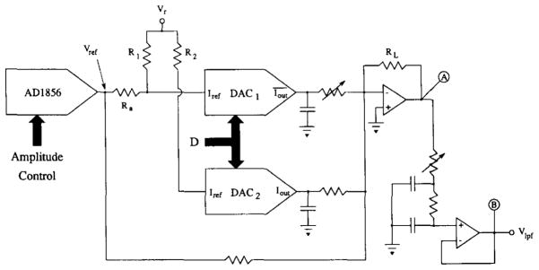
Conversion of the digital waveform data into a variable-amplitude analog signal is accomplished by a multiplying digital-to-analog converter (MDAC) system. The transfer equation of a current steering, R–2R ladder MDAC with η bits of resolution is given by
where d0 ⋯ dη−1 ≡ D is the digital input, Vref is the analog reference input, and Vout is the analog output voltage. The output of the MDAC is a current which is then input to an op amp current-to-voltage converter with transresistance –K.
One interpretation of the transfer equation is that the analog reference signal is attenuated by the value of D. However, the output impedance of the MDAC device is a nonlinear function of the value of D [5]. The op amp current-to-voltage converter following the MDAC is not ideal, but rather, has a finite bandwidth and nonzero input impedance. Therefore, the modulation of the MDAC output impedance causes a phase shift in Vout which depends upon D, and hence upon the amplitude of Vout.
To eliminate this dependence of output phase shift upon output magnitude, the roles of Vref and D are swapped: D now represents a sequence of quantized sinusoid samples and Vref the scaling factor. Vref is a dc signal, provided by a slow, high-resolution DAC with a constant reference, such as Analog Devices’ AD1856. The benefit of this interchange is that the amplitude-dependent phase shift is replaced by signal distortion, which is independent of amplitude. The amount of distortion can be reduced by using an op amp with a large gain–bandwidth product, so that the open-loop phase shift is small at the sinusoid’s frequency. The distortion is also decreased by utilizing bipolar MDAC devices which have smaller switch capacitances and are, therefore, faster than corresponding CMOS devices. Furthermore, the amplitude resolution is increased economically since it is the inexpensive, high-resolution AD 1856 that controls the amplitude.
Bipolar MDAC’s are only two-quadrant devices; while their output can be of either polarity, their reference input must always be positive for proper operation. To produce a sinusoid whose magnitude may be positive or negative (negative magnitudes are equivalent to a 180° phase shift) requires a four-quadrant MDAC subsystem, such as that shown in Fig. 4. This can be accomplished by subtracting the outputs of two two-quadrant devices, DAC1 and DAC2, with identical digital inputs D, such that device DAC2 has a fixed , while for DAC2, . Analog Devices’ 10 b, two-quadrant DAC10 provides both normal (I0) and complementary (Ī0) current outputs, related according to I0 + Ī0 = 2(1023/1024)Iref. Thus, the subtraction function can be realized by connecting the normal output of DAC1 and the complementary output of DAC2 to the summing node of the op amp current-to-voltage converter. Because each DAC10 is a two-quadrant device, the outputs of both DAC1 and DAC2 are in phase. Therefore, when Vref = 0, the two outputs cancel, resulting in zero output. When Vref > 0, the output amplitude of DAC1 is larger than that of DAC2, and the output has a phase of 180°. Conversely, when Vref < 0, the output amplitude of DAC1 is smaller than that of DAC2, and the output has a phase of 0°. The peak-to-peak value of the voltage at point A in Fig. 4, under the condition that R1 = R2, is given by [4] VA\p–p = 2RL(Vref/Ra). The RC networks placed on the output of DAC1 and DAC2 equalize the phase of the output currents from the two DAC’s. Phase differences as large as 0.010° have been measured between devices. The variable pole placed at the output of DAC1 allows for ±0.013° of phase adjustment relative to the output of DAC2. Finally, since this circuit implements a zero-order data hold, a two-pole low-pass filter is placed at the output to smooth the step discontinuities. Adjustment of the location of the filter poles is afforded by a potentiometer to accommodate interchannel phase differences.
Fig. 4.
Details of the voltage waveform source circuit for one channel—nodes labeled A and B are also shown in Fig. 3.
2) Current Source
The filtered output of the voltage waveform source is converted to a current which is then applied to the electrode by the current converter subsystem. As shown in Fig. 3, this subsystem consists of a voltage-to-current converter and an output impedance compensation and calibration network, both under computer control.
An important specification of a current source is its output impedance Zout, which appears in parallel with the load Zl connected to the current source output. A finite output impedance shunts current away from the load. Since Zl is unknown, a finite output impedance causes an error to exist between Iin, the current that is sourced, and Iload, the current applied to the load. In addition to causing errors in the reconstructed image, this disparity between sourced and applied current leads to errors in system calibration.
Since ACT3 is designed to image both the resistive and reactive parts of Z(p), Zout must be sufficiently large to limit error in the magnitude and phase of the applied current. To maintain an applied current accuracy of 1 part in 216 in both the real and reactive channels, assuming a load with impedance 0–1 kΩ and phase angle between 0° and 90°, the impedance of both the resistive and reactive part of Zout must exceed 64 MΩ, so that |Rout| ≥ 64 MΩ and |Cout| ≤ 0.083 pF [8].
The current source used in ACT3 is shown in Fig. 5. The current output to the electrode is given by
where the instrumentation amplifier (IA) gain Av is assumed to have the form Av ≡ A0/1+j(ω/ωc). Here, A0 is the dc gain of the IA and ωc is the dominant pole. If the IA has infinite bandwidth and unity dc gain, then Rout = ∞ and Cout = 0 so that Zout = ∞—the ideal case. Even for an amplifier with finite bandwidth, however, it is possible to cause either Rout → ∞ or Cout → 0, but not both, by an appropriate choice of A0. For the former, for example, A0 must be chosen such that [4]
Fig. 5.
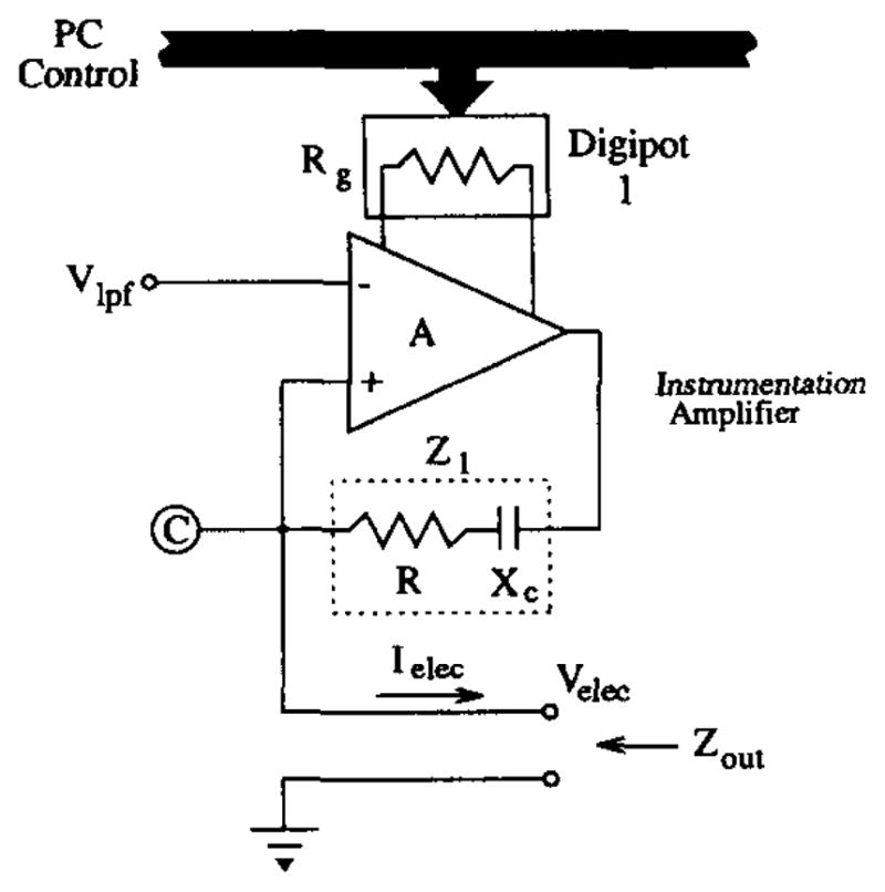
The design concept for an instrumentation amplifier-based voltage-to-current converter—node C also appears in Fig. 3.
| (9) |
For an amplifier with a small phase shift at 30 kHz, the gain A∞ is very nearly 1.0. Usually, IA’s are fabricated with internal gain-setting resistors chosen for large gains—a gain of 1.0 is somewhat unusual for such a device. However, one device that allows the gain to be set by external resistors is Analog Devices’ AMP05. This device has a bandwidth of ωc = 2π × 106 rad/s for A0 = 1.0, so that the phase shift at 30 kHz is small. The dc gain expression for the AMP05 is
| (10) |
A convenient means of adjusting this gain is afforded by realizing the gain setting resistor Rgain by a digitally programmable potentiometer whose value is under computer control.
The current source output capacitance can be nulled by a negative capacitance circuit, such as shown in Fig. 6 [13]. Analysis of this circuit assuming an op amp with open-loop gain A yields an input impedance of3
Fig. 6.
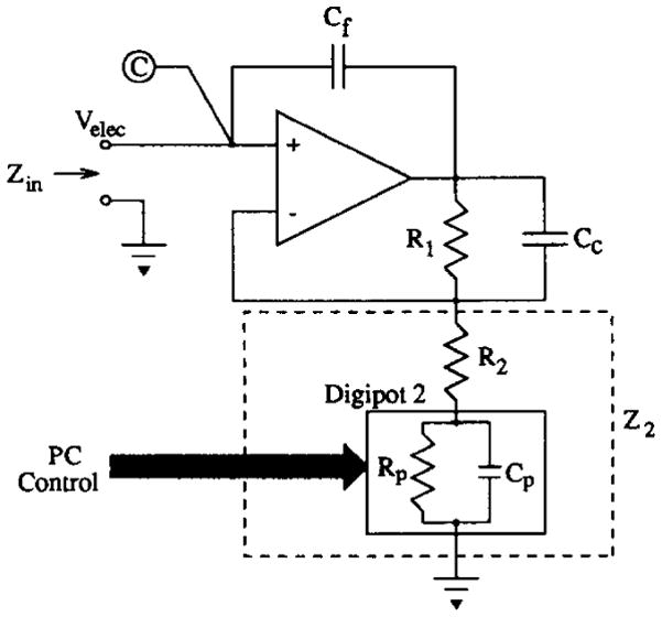
Conceptual schematic for the negative capacitance circuit used in ACT3. Node C also appears in Fig. 3.
The input capacitance of this circuit is adjusted by varying the digitally programmable potentiometer Rp. Fig. 7 shows plots of input resistance and capacitance under the assumption that the op amp has an open-loop dc gain of 100 dB and a dominant pole at ωc = 157 rad/s.
Fig. 7.
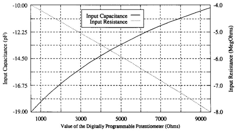
Increases in the value of the digitally programmable potentiometer produces larger negative values of input resistance and smaller negative values of input capacitance.
Since the output capacitance of the current source is usually negative, a capacitor is put in parallel with its output to make a positive net capacitance. The negative capacitance circuit is then used to null the overall capacitance. Additionally, note that the adjustments to peak output resistance and null output capacitance are not orthogonal since adjusting the output resistance changes the output capacitance and vice versa. The algorithm used to peak the total output impedance, then, has to simultaneously adjust both output resistance and capacitance.
3) Automatic Impedance Trim and System Calibration
The use of computer-controlled potentiometers to independently control the current source output resistance and capacitance allows for implementation of an automatic routine to trim the output impedance of the current source. For accurate and efficient impedance trimming, an algorithm is required which determines the direction and amount by which both potentiometers must be changed. Furthermore, a measurement scheme is required to provide this algorithm with the appropriate data. ACT3 uses a resistive droop technique, which works on the principle that the current through a load resistor connected between the current source output and ground depends upon the value of that resistor if the output impedance of the current source is finite. Thus, the output resistance and capacitance can be determined by measuring the amount by which the currents through two different but known loads, denoted and , differ. The resistive droop measurement scheme is shown in Fig. 8 where . Vcal, the op amp output voltage, is proportional to the current flowing through the load resistors.
Fig. 8.
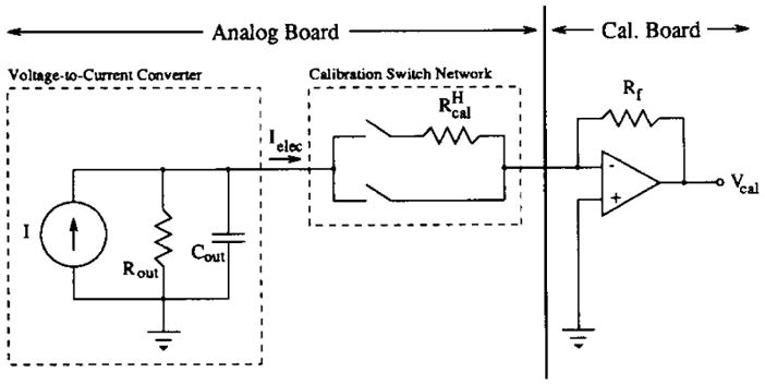
The circuit used to measure current source output impedance.
Define the voltages measured for the two calibration loads as
Then [4],
| (11) |
| (12) |
Notice that Cout → 0 and Rout → ∞ if and only if and . Automatic trimming of the digipots can be performed by noting the effect of the potentiometer settings upon Rout and Cout, computed by (12) and (11), respectively.
Measurement of and is performed by a calibration system, centrally located within the ACT3 instrument. In addition to the current-to-voltage converter shown on the right of Fig. 8, the calibration system contains a phase-sensitive voltmeter and voltage waveform source as described previously. A mode-switching network between these three units allows the calibration system to be used for the automatic output impedance trimming procedure and for automatic system calibration. As indicated in Fig. 3, point C on each analog board may be connected to the calibration board via the calibration switch network. The calibration board can measure the current output by the analog board for measurement of and and for calibration of the voltage-to-current converter. Also, the calibration board can apply a reference sinusoid to point C on each analog board for calibration of the phase-sensitive voltmeters. In this way, all system calibrations are performed with respect to the centrally located calibration system, which ensures system self-consistency.
III. Test Results
A. System SNR
The measured system SNR is computed based on a large number L of measurements of the voltage v(l) appearing at an electrode as a result of the application of a constant-magnitude current. The SNR can be computed by forming the ratio of the mean-squared value of these voltage measurements to the variance of the measurements
| (13) |
The experimentally determined SNR’s for all 32 electrodes, computed with L = 465, are plotted in Fig. 9. The mean of the experimentally measured SNR’s is 105.1 dB, while the minimum SNR measured is 104.0 dB. It must be noted that these data are obtained by applying a maximum amplitude current (500μA) to a 1 kΩ load, thereby resulting in a maximum amplitude sinusoid input to the voltmeter. In this way, the maximum experimental SNR of the instrument is obtained.
Fig. 9.
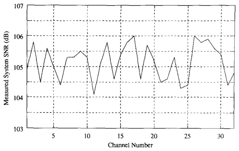
The signal-to-noise ratio exceeded 104 dB for all channels when studied using full-scale output currents and 1000 Ω (maximum) loads.
To demonstrate the accuracy of the ACT3 system, another test was performed on each channel. A sinusoidal current, with an amplitude of 500 μA, was applied to a known resistor (497.717Ω) connected one at a time to each channel. The voltage across the resistor was measured using each channel’s voltmeter. The mean resistance calculated from these measured data for all channels was 495.11Ω with a standard deviation of 0.12Ω. These data demonstrate an absolute accuracy for the ACT3 system of approximately 99.5% and a coefficient of variation of 0.024%. The variations among channels are a function of the system calibration accuracy, as well as dissimilarities among channels including electode lead resistance.
B. Current Source Output Impedance
The output resistance and capacitance are both monotonic functions of the values of the respective computer-controlled potentiometers. The output impedance will therefore have a unique maximum if the output resistance and capacitance are maximized and minimized, respectively, within the available potentiometer range, and an automatic trimming routine based on a bisection algorithm [4] will ultimately select potentiometer settings which yield this maximum impedance.
Fig. 10 shows an example of an experimentally determined current source output impedance surface, measured by the resistive droop technique. The values of the digitally programmable potentiometers are defined by an 8 b digital word; the x and y axes of the plot represent the values of the digital words, or steps, for the Rout and Cout compensating potentiometers. the output impedance peak extends to about 100 MΩ; the region of potentiometer settings that results in an output impedance of at least 64 MΩ is 2 × 2 potentiometer steps.
Fig. 10.
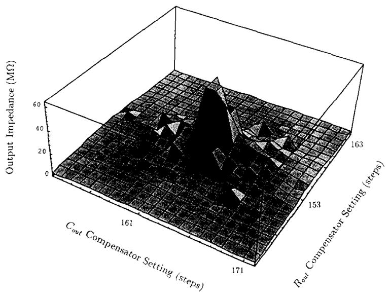
Current source output impedance exceeded 50 MΩ for at least four pairs of settings of the Rout and Cout compensators.
The output impedance peak cannot be expected to persist indefinitely at a given potentiometer pair setting since temperature changes and aging which affect component values will cause the output impedance peak to drift with time. For example, the output impedances for all 32 channels were found to be above 50 MΩ immediately following an automatic trimming procedure, with all but one channel having an output impedance in excess of 64 MΩ. After the instrument had been powered down for approximately 16 h and then allowed to warm up for 1.5 h, none of the 32 channels exhibited an output impedance in excess of 25 MΩ. Following another automatic trimming procedure, however, the output impedances for all channels again exceeded 50 MΩ. All channels maintained this high output impedance for 1 h after the trimming procedure; long-term adherence to the 64 MΩ output impedance requirement requires periodic trimming.
IV. ACT3 Images
Since the purpose of ACT3 is to provide the reconstruction algorithm [3] with the data necessary to compute an image of the electrical impedance distribution, perhaps the best way to qualify ACT3’s performance is to demonstrate the images produced. Of course, image quality is a function of the reconstruction algorithm as well as the ACT3 hardware.
A. Finite Contrast, Static Images
For test purposes, a tank of diameter 30 cm and height 5 cm has been constructed. Equally spaced around the circumference of the tank are 32 stainless steel electrodes, whose height and width are 2.54 cm. The tank is filled with saline of known conductivity, in which are placed targets of known conductivities and geometries. Reconstructed images can then be compared to this known impedance distribution. The current patterns used here are the trigonometric patterns; the adaptive current algorithm is not used [10].
In order to verify the imaging process, the tank was filled with saline of resistivity 607Ω · cm. A 46 g/L solution of agar in saline was prepared and allowed to gel in two cylinders of depth 2.54 cm and diameters of 9.0 and 4.4 cm. The resistivity of the agar cylinders at room temperature was measured and found to be 153Ω · cm, so that the ratio of background saline-to-target resistivity is 4.0. The two agar targets were placed in the tank, with their centers located halfway along the tank’s radius. The 4.4 and 9.0 cm diameter targets were placed at angular displacements of 90° and 135°, respectively. The voltage data were obtained for this target placement, and the resulting reconstructed image is shown at the left in Fig. 11; to the right of this image is shown the actual target placement. Clear in this image are the two agar targets, at the correct locations. The average reconstructed resistivity of the saline bath is approximately 500Ω · cm—a 17.6% error from the correct value of 607 ω · cm. Furthermore, while the two agar targets are clearly visible in the reconstructed image, their reconstructed resistivities are in error. The reconstructed 9.0 cm target shows a peak deviation from the saline background of 87 Ω · cm, while the 4.4 cm target shows a deviation of only 18.5 Ω · cm. These reconstructed values represent errors of 42 and 87.7%, respectively, from the actual value of 150 Ω · cm, a characteristic of the reconstruction algorithm.
Fig. 11.
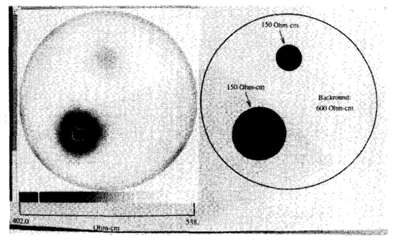
Reconstructed image of two agar targets having 150 Ω · cm resistivity located in a saline bath with a background resistivity of 600 Ω · cm.
Note that the image shown in Fig. 11 is an unsubtracted one; most EIT systems presently implemented require that a reference background image be algebraically subtracted from the target image, resulting in a subtracted image. The advantage of an unsubtracted image is that true values of resistivity and permittivity may be obtained. A disadvantage of unsubtracted images is that they are sensitive to errors introduced both by imperfect hardware calibration and by the reconstruction algorithm errors resulting from imperfect electrode modeling. For example, note the highly conductive (dark) layer at the boundary in Fig. 11. this phenomenon is absent in a subtracted image.
B. Pendulum Sequence
To demonstrate the imaging resolution and speed of the ACT3 system, a pendulum was formed from a weighted 8 mm diameter copper rod suspended by a 2 m long cord and allowed to swing across the diameter of the saline phantom. Since ACT3 can collect data for 14 images in 2 s, it can record 0.7 periods of this 2.8 s pendulum. The first eight images from such a sequence are shown in Fig. 12. This is a sequence of subtracted images since the errors due to incorrect electrode modeling and nonidealities of the phantom are large compared to the signal generated by this small target. A data set was therefore obtained from the homogeneous tank, and subtracted from each frame of the original sequence, resulting in the images shown in the figure.
Fig. 12.
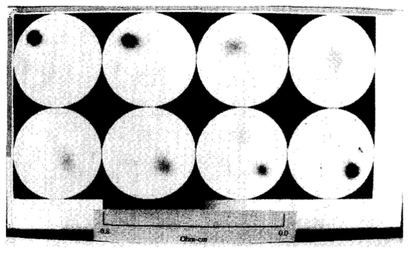
Sequence of eight images of an 8 mm diameter copper pendulum swinging through a saline phantom—images are separated by 133 ms.
Although the path of the pendulum is clear from the image sequence, the image of the 8 mm copper cylinder is blurred, and significantly larger than the cylinder itself. The full-width at half-maximum (FWHM) of the resistivity profile through the target is 14% of the phantom diameter when the pendulum is positioned at a radial distance equal to half of the radius. The reconstructed images in Fig. 12 appear larger than the actual target due to the broad point-spread function of the reconstruction algorithm, not due to properties of the data collection hardware.
Another feature of the reconstruction algorithm is that as the pendulum approaches the center of the tank, its image contrast is reduced. This is a manifestation of the decrease in distinguishability [10] as the distance from the object to the electrode array increases. Despite these shortcomings, these images provide evidence of the speed and precision of the data collection system.
C. In Vivo Respiration Sequence
A second demonstration involved in vivo studies on a human subject, imaging the events of pulmonary ventilation. An electrode array was attached around the chest of the subject. A detailed description of the electrode array properties and subject preparation are given in [12] and [11], respectively.
As with the pendulum experiment, data were collected in 14 frame sequences. However, a 150 ms delay was added between frames, slowing the acquisition rate to 3.5 frames/s and allowing 4 s for the respiratory maneuvers. The subject triggered the start of data acquisition manually, and observed the polygraph record to achieve the desired tidal volume. Data acquisition was started at Functional Residual Capacity (FRC). During the next 2 s, inspiration occurred at a rate of 0.85 L/s until the tidal volume reached about 1.3 L, after which the subject expired at the same rate until the inspired volume was reduced to 0.6 L.
The sequence of unsubtracted images [11] shows a peripheral layer of high resistivity (245–315 Ω · cm), which is attributed to skin and fat. Interior to this peripheral layer are bilateral regions of lower resistivity 150–200 Ω · cm). With inspiration, the resistivity of these regions increased. The average resistivity within these two regions of interest increased by 4.5%/L of inspired gas on the right and 5.2%/L on the left (Fig. 13). The absolute values of resistivity, particularly for centrally located structures, is artifactually reduced by the presence of out-of-plane currents. The actual resistivity of lung tissue is 1000–2000 Ω · cm. The values reported here are reduced by the added currents flowing above and below the electrode plane, which are not modeled by the reconstruction algorithm.
Fig. 13.
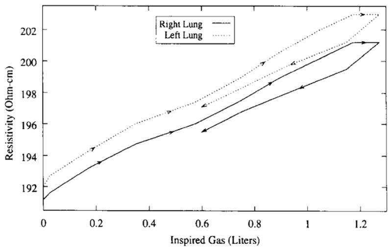
Plot of the average resistivity in both lung fields as air is imspired and expired, starting at Functional Residual Capacity—data points were obtained every 290 ms for 4 s.
V. Conclusions
The ACT3 instrument has been demonstrated to meet the design goals of having 16 b precision on both the current values and real and reactive voltage measurements. This precision was obtainable by implementing the phase-sensitive voltmeter and 30 kHz sinusoid generation using digital rather than analog techniques. System accuracy is maintained to a similar specification by incorporating automatic current source output impedance compensation and automatic system calibration features.
Acknowledgments
This work was supported in part by NIH Grants GM39388, RR-07104, and GM 42935 and by NSF Grant EET8706340.
We would like to thank Analog Devices Inc., Norwood, MA, for providing components; without their help, we could not have built an instrument as fast and accurate as ACT3. We would also like to thank C. McLeod of Oxford Polytechnic, UK, for early discussions concerning the system DSP architecture. Prof. M. Cheney has contributed significantly to the theoretical basis for EIT research at RPI. Finally, we wish to thank L. Carlyle for writing much of the high-level system software.
Biographies

Raymond D. Cook was born in Fairfax, VA, in 1966. He received the B.S. degree in biomedical engineering in 1988, the M.S. degree in biomedical engineering in 1991, and the Ph.D. degree in biomedical engineering with an emphasis in electrical engineering in 1992, all from Rensselaer Polytechnic Institute, Troy, NY.
From 1988 to 1992 he worked as a Research Assistant in the Department of Biomedical Engineering at Rensselaer Polytechnic Institute. His research interests included multidimensional signal processing, electrical impedance tomography, and high-speed analog and digital circuit design.
Gary J. Saulnier (S’80–M’84) was born in Fall River, MA. He received the B.S., M.E., and Ph.D. degrees in electrical engineering from Rensselaer Polytechnic Institute, Troy, NY, in 1980, 1982, and 1985, respectively.
In 1984 he joined General Electric Corporate Research and Development Center, Schenectady, NY, where he studied the design and implementation of bandwidth-efficient digital modulation techniques for fading channels. Since 1986 he has been on the faculty of the Electrical, Computer, and Systems Engineering Department at Rensselaer Polytechnic Institute, where he is currently an Associate Professor. His research interests include modems for mobile and mobile-satellite channels, antijam spread spectrum systems, and electronic instrumentation for biomedical applications.
David G. Gisser (S’41–M’47) was born in Kingston, NY, on December 6, 1922. He was educated in electrical engineering at Rensselaer Polytechnic Institute, Troy, NY, and received the D.Eng. degree in 1965.
He has been a member of the faculty of Rensselaer Polytechnic Institute since 1947. Currently, he is a Professor Emeritus in the Department of Electrical, Computer, and Systems Engineering. His research interests have been largely in the area of measurement instrumentation, as applied to many fields, especially nuclear and biomedical. He is coauthor of a textbook, Electrical Engineering: Concepts and Applications, as well as many papers.
Dr. Gisser is the recipient of a number of honors, notably an IEEE Centennial medal. He is a past Chairman of the Schenectady Section of IEEE and served for 20 years as Student Branch Counselor at Rensselaer Polytechnic Institute.

John C. Goble received the Ph.D. degree in computer science from Rensselaer Polytechnic Institute and the Sc.M. degree in radiological physics from The Johns Hopkins University.
He is currently an Assistant Professor in the Departments of Neurological Surgery and Biomedical Engineering at the University of Virginia, and Director of the Neurosurgical Visualization Laboratory. His present research focuses on the application of advanced computer and communications technologies to the academic and clinical efforts of the neurosurgeon. Current work in his lab includes knowledge-based image segmentation algorithms, 3D user interface design, fast volumetric rendering, and inverse radiosurgical planning techniques.
J. C. Newell (M’74) received the B.S. and M.S. degrees in electrical engineering from Rensselaer Polytechnic Institute, Troy, NY, where he graduated in 1968, and the Ph.D. degree in physiology from Albany Medical College, Albany, NY, in 1974.
He was with the Missile Systems Division of Raytheon Company before joining the Powers Trauma Research Center at Albany Medical College as a Biomedical Engineer in 1970. He is now Professor of Biomedical Engineering at Rensselaer Polytechnic Institute and Professor of Physiology and Surgery at Albany Medical College. His research interests have included the regulation of the pulmonary circulation in hypoxia, and pulmonary gas exchange in injured patients with acute respiratory failure. His recent work has been the development of an adaptive system for electrical impedance imaging.
David Isaacson (M’86) received the Ph.D. degree in mathematics from New York University’s Courant Institute of Mathematical Sciences in 1976.
He is a Professor of Mathematics at Rensselaer Polytechnic Institute, Troy, NY. He is currently working on problems arising in the use of electro-magnetic fields for the diagnosis and treatment of disease.
Footnotes
Knowledge of Vr and Vq is equivalent to knowledge of magnitude (M) and phase (ϕ) since the latter can be obtained from the former by means of a Cartesian-to-polar transformation.
To decrease system cost, high-speed, low-resolution (12 b) ADC’s are used to sample the voltage. Quantization noise from such devices dominates the noise introduced by low-noise analog circuitry and sampling uncertainty. A complete treatment of voltmeter SNR degradation due to all of these noise sources is given in [4].
The symbol “Za || Zb” denotes the parallel combination of the two impedances Za and Zb.
IEEE Log Number 9402538.
Contributor Information
Raymond D. Cook, Department of Biomedical Engineering, Rensselaer Polytechnic Institute, Troy, NY 12180 USA
Gary J. Saulnier, Department of Electrical, Computer, and Systems Engineering, Rensselaer Polytechnic Institute, Troy, NY 12180 USA.
David G. Gisser, Department of Electrical, Computer, and Systems Engineering, Rensselaer Polytechnic Institute, Troy, NY 12180 USA.
John C. Goble, Department of Neurosurgery, University of Virginia, Charlottesville, VA 22903 USA
JC. Newell, Department of Biomedical Engineering, Rensselaer Polytechnic Institute, Troy, NY 12180 USA.
David Isaacson, Departments of Mathematics and Computer Science, Rensselaer Polytechnic Institute, Troy, NY 12180 USA.
References
- 1.Brown B, Barber D, Jossinet J, editors. Clinical Physics and Physiological Measurement. Commission of the European Communities COMAC–BME Workshop. 1988 Oct;9(suppl A) [PubMed] [Google Scholar]
- 2.Brown B, Barber D, Tarassenko L, editors. Clinical Physics and Physiological Measurement. Commission of the European Communities COMAC–BME Workshop. 1987 Jul;8(suppl A) [PubMed] [Google Scholar]
- 3.Cheney M, Isaacson D, Newell JC, Simske S, Goble J. NOSER: An algorithm for solving the inverse conductivity problem. Int J Imaging Syst Technol. 1990 doi: 10.1002/ima.1850020203. [DOI] [PMC free article] [PubMed] [Google Scholar]
- 4.Cook RD. PhD dissertation. Rensselaer Polytechnic Inst; Troy, NY: 1992. ACT3: A high-speed, high-precision electrical impedance tomograph. [Google Scholar]
- 5.Cook RD. Master’s thesis. Rensselaer Polytechnic Inst; Troy, NY: 1992. A high speed, low phase distortion four quadrant multiplying DAC. [Google Scholar]
- 6.Defatta DJ, Lucas JG, Hodgkiss WS. Digital Signal Processing: A System Design Approach. New York: Wiley; 1988. [Google Scholar]
- 7.Edic PM. Ground current monitor for ACT3. RPI Internal Paper. 1991 [Google Scholar]
- 8.Gisser DG, Newell JC, Goble JC, Cook RD, Hochgraf C. Current sources for impedance imaging systems. Proc 12th Annu Int Conf, IEEE Eng Med Biol Soc. 1990:112–113. [Google Scholar]
- 9.Hames TK, editor. Proc Meet Elec Impedance Tomography. European Community Concerted Action on Electrical Impedance Tomography; Jul, 1990. [Google Scholar]
- 10.Isaacson D. Distinguishability of conductivities by electric current computed tomography. IEEE Trans Med Imaging. 1986;MI-5(2):91–96. doi: 10.1109/TMI.1986.4307752. [DOI] [PubMed] [Google Scholar]
- 11.Newell JC, Isaacson D, Cheney M, et al. In-vivo impedance images using sinusoidal current patterns. Proc 14th Annu Int Conf, IEEE Eng Med Biol Soc. 1992 [Google Scholar]
- 12.Newton C. Master’s thesis. Rensselaer Polytechnic Inst; Troy, NY: 1992. In vivo electrodes for electrical impedance imaging. [Google Scholar]
- 13.Roberge JK. Operational Amplifiers: Theory and Practice. New York: Wiley; 1975. [Google Scholar]
- 14.Webster JG, editor. Electrical Impedance Tomography. Adam Hilger; 1990. [Google Scholar]


