Abstract
Manipulating electronic and magnetic properties of two-dimensional (2D) transitional-metal dichalcogenides (TMDs) MX2 by doping has raised a lot of attention recently. By performing the first-principles calculations, we have investigated the structural, electronic, and magnetic properties of transitional metal (TM)-doped MoS2 at low and high impurity concentrations. Our calculation result indicates that the five elements of V-, Mn-, Fe-, Co-, and Cu-doped monolayer MoS2 at low impurity concentration all give rise to the good diluted magnetic semiconductors. By studying various configurations with different TM-TM separations, we found that the impurity atoms prefer to stay together in the nearest neighboring (NN) configuration, in which the doped TM atoms are FM coupling except for Fe doping at 12 % concentration. For V, Mn, and Fe doping, the total magnetic moment is smaller than the local magnetic moment of the dopants because the induced spins on the nearby host atoms are antiparallel to that of the doped atoms. In contrast, Co and Cu doping both give the higher total magnetic moment. Especially, Cu doping induces strong ferromagnetism relative to the local spins. However, the atomic structures of Co- and Cu-doped MoS2 deviate from the original prismatic configuration, and the magnetic moments of the doped systems decrease at 12 % impurity concentration although both elements give higher magnetic moments at 8 % impurity concentration. Our calculations indicate that V and Mn are promising candidates for engineering and manipulating the magnetism of the 2D TMDs.
Electronic supplementary material
The online version of this article (doi:10.1186/s11671-016-1376-y) contains supplementary material, which is available to authorized users.
Keywords: MoS2, Transitional metal, Doping, Magnetic interaction, First-principles calculations
Background
Research on two-dimensional (2D) transitional metal dichalcogenides (TMDs) has attracted considerable attention due to their distinct electronic, optical, and catalytic properties [1–5]. Group 6 TMDs (MX2, M = Mo, W, and X = S, Se, Te) hold promise for flexible and transparent electronics applications owing to their sizeable band gaps ranging from 1 to 2 eV. Current results have indeed revealed that MoS2 and WS2 form an exciting family of transistors [6–11]. On the other side, MoS2 and WS2 are nonmagnetic semiconductors. Accordingly, extensive studies have been performed to investigate the feasible ways to introduce magnetism to MoS2, such as morphology fabricating [12–14], external strain, [15–17] and impurity doping [18–28].
Developing approaches to effectively induce and manipulate magnetism are critical to the use of the magnetic nanostructures in quantum information devices. Among kinds of magnetic property engineering methods, doping attracts more attentions [18–28]. On the basis of previous studies, transitional metal (TM) atom doping can effectively induce magnetism into MoS2. For example, magnetism is observed for Mn [18, 20, 22, 24, 26, 28], Fe [18, 22, 24, 26, 28], Co [18, 22, 24, 26, 28, 29], Cr [18, 24], Zn [22, 24], Cd [24], and Hg [24] doping. And the magnetic moment of the 3d TM-doped MoS2 increases with the d-band filling of the TM dopants [18]. Additional, spin polarization was found in MoS2 with S atoms replaced by incomplete d-band atoms, such as Fe and V [30], and Group VA and III elements, such as N, P, As, B, Al, and Ga [28]. Moreover, adsorption of various atoms, such as H, B, C, N, and F, is also effective to turn MoS2 from nonmagnetic to magnetism [31]. It is worth noting that no magnetism is observed in V-doped MoS2 based on Ref [24], but according to Ref [18] and [28], V doping induces more than 1-μB magnetic moments into monolayer MoS2. And based on Lee’s study [22], the nonmagnetic element Cu doping brings strong magnetism into the doped MoS2.
More recently, substitutional doping MoS2 monolayer with magnetic atom and the interactions between the doped atoms has draw intensive attentions. Ramasubramaniam [20] have studied the Mn-doped monolayer MoS2 at concentration of 10–15 % by performing the density functional theory calculations and Monte Carlo simulations, which shows that the doped Mn atoms couple ferromagnetically. Schwingenschlögl et al. [24] predict that the doped TM atoms are ferromagnetic (FM) ordering for Mn, Zn, Cd, and Hg doping at 6.25 % impurity concentration and antiferromagnetic (AFM) ordering for Fe and Co doping. Similarly, Mishra et al. [26] predict the FM ordering in fairly diluted Mn doping MoS2, MoSe2, MoTe2, and WS2 and AFM coupling for Fe and Co doping at large separations. In contrast, a later study [18] found the ground states of Mn-, Fe-, and Co-doped MoS2 are all FM.
Clearly, current studies on the magnetic interactions in Mn-, Fe-, and Co-doped MoS2 disagree with each other. However, the magnetic ordering of the dopants as well as the orientations of the induced spins on the host atoms are critical factors to determine the magnetic property of the doped system. In this context, we examined the cases of different impurity concentrations and separations of the doped atoms to study the electronic and magnetic properties of TM-doped monolayer MoS2 and to find out the magnetic feature of the TM-doped 2D TMDs. Five 3d TM elements including V, Mn, Fe, Co, and Cu doping were studied in the present work by accurate calculations. Our calculations result indicates that the doped TM atoms prefer to stay in the nearest neighboring configurations and ferromagnetic coupling with each other. Additionally, we found that at high impurity concentrations, the local structures around the dopants were deformed from the original prismatic configurations. More importantly, it was found that V and Mn doping are the good candidate to induce and manipulate the magnetism into 2D TMDs, but Cu is not although it can induce strong magnetism.
Methods
The first-principles calculations were carried out by using the Vienna ab initio simulation package (VASP) based on the density functional theory (DFT) [32]. The electron-ion interactions were described by the projector-augmented wave (PAW) method [33, 34]. The generalized gradient approximation of the Perdew-Burke-Ernzerhof (PBE-GGA) [35] formula was used for the electronic exchange-correlation potential. In addition, Hubbard-U parameterization method with a common U value of 3.0 eV was assigned to all the 3d impurities. The U parameterization was not used for the host materials since there little impact on the magnetic ordering [18, 26, 36]. The substitutional TM doping was calculated with a 5 × 5 × 1 supercell. A vacuum region of 15 Å was added to avoid interactions between adjacent images. The Brillouin zone was sampled by the Monkhorst-Pack method [37] with a 2 × 2 × 1 k-point grid. The wave functions were expanded in a plane wave basis with an energy cutoff of 600 eV. The convergence criterion for the self-consistency process was set to 10−5 eV between two ionic steps, and the convergence criteria of 0.02 eV/Å were adopted for total energy calculations.
Results and Discussions
The fully relaxed lattice constants are a = b = 3.18 Å for single layer MoS2, and the distance between Mo and S atoms are 2.41 Å. Figure 1 shows the atomic structure and density of states for monolayer MoS2, which is nonmagnetic semiconductor. Our calculated band gap is 1.70 eV with the valence band maximum and conduction band minimum both locating at Κ point. Morphology fabricating such as atomic defects is a useful way to bring ferromagnetism into the low-dimensional materials [38, 39]. But according to previous study [17, 40], neither Mo vacancy nor S vacancy changes the nonmagnetic property of monolayer MoS2. Also, Si vacancy does not bring magnetism into silicene [41, 42]. As shown in Fig. 1, our calculation shows the same results.
Fig. 1.
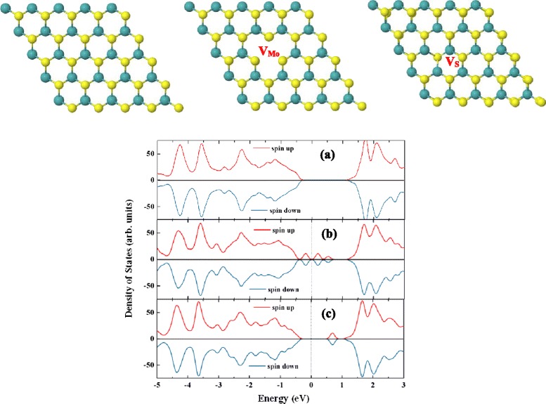
Top views and density of states of monolayer MoS2 without and with Mo/S vacancy. Density of states of monolayer MoS2 (a), monolayer MoS2 with Mo vacancy (b), monolayer MoS2 with S vacancy (c)
We firstly studied the doping at low impurity concentration. The doping concentration is defined as the number of doped TM atoms divides by the total number of Mo atoms. Hence, if one Mo atom is replaced by one TM atom in a 5 × 5 × 1 supercell, the corresponding impurity concentration should be 4 %. The formation energies of TM substitutional doping MoS2 are calculated via the following formula:
where E(TMMo, MoS2) and E(MoS2) represent the total energies of MoS2 with and without TM doping, respectively. μTM is the chemical potential of a single-doped TM atom in its stable bulk lattice. For Mo-rich condition, μMo is taken as the energy of a Mo atom in its stable fcc lattice and for S-rich condition μMo is determined from the energy difference between a S2 molecule and one MoS2 unit. Figure 2 shows our calculated formation energies for TM doping MoS2 as a function of μMo. It shows that the V and Mn doping are favorable energetically, especially under S-rich growth conditions. The C3v symmetry is destroyed after TM doping, and the distances between the doped TM and the nearest S atoms are 2.39, 2.36 2.44, 2.30, and 2.42 Å for V, Mn, Fe, Co and Cu doping.
Fig. 2.
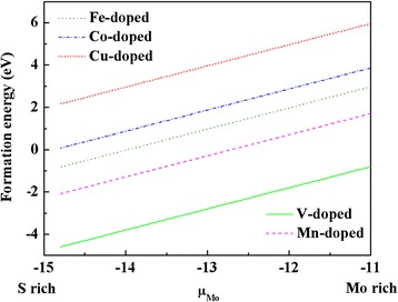
Formation energies for TM atom substitutional doping MoS2 as a function of chemical potential of Mo (μMo)
Figure 3 shows our calculated DOSs for TM-doped monolayer MoS2 at 4 % impurity concentration. As shown in Fig. 3, defect states appear within the band gap for all the doped systems and they are highly localized. The defect states are mainly contributed by the doped TM 3d states. Additionally, for the V-, Mn-, Fe-, and Cu-doped systems, both the defect states and Fermi level are more close to the valence band, but for the Co-doped system, the impurity level and Fermi level are more close to the conduction band. This is different from previous result by Lebruton et al. [28] Based on their DFT/PBE calculations, they have predicted that for Mn-, Fe-, and Co-doped MoS2, the impurity level and Fermi level both are more close to the conduction band. However, as shown in Additional file 1: Figure S1, our calculations result with no U parameterization which agrees with the results of Leburton et al. [28] and Lee et al. [22]. Moreover, all the doped systems are still semiconductor although the band gaps reduce a lot relative to the original value before doping.
Fig. 3.
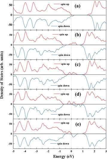
Density of states of monolayer MoS2 with V, Mn, Fe, Co, and Cu doping at 4 % impurity concentration. a V doping, b Mn doping, c Fe doping, d Co doping, e Cu doping
More importantly, Fig. 3 clearly shows the induced spin polarization for all the five doped systems. The corresponding magnetic moments are 1, 1, 2, 3, and 4.9 μB for V, Mn, Fe, Co, and Cu doping, respectively. An isolated V atom has a 3d44s1 electronic configuration with one valence electron less than Mo (4d55s1), which reflects the magnetic moment of the V-doped MoS2. The electronic configurations of isolated Mn, Fe, Co, and Cu atom are 3d54s2, 3d64s2, 3d74s2, and 3d104s1, respectively; they have one, two, three, and five additional valence electrons compared to Mo atom, which consist with the magnetic moment of Mn-, Fe-, Co-, and Cu-doped system. As shown in Fig. 3, the spin splitting appears near to the Fermi level, which is contributed by the defect states associated with the doped TM atom, p states of the adjacent S atoms, and d states of the nearby Mo atoms. We further calculated the spin-resolved charge density to investigate the distribution of these magnetisms.
As shown in Fig. 4, we can see the spin polarization localized on the dopants and the nearby S and Mo atoms, as well as the interstitial region. Strong hybridization between the TM 3d states and the p states of the adjacent S atoms yields spin splitting to the S atoms. For V and Mn doping, the spins of the dopants are antiparallel to the induced spin of the nearest three S atoms. In V-doped MoS2, the induced spins on the nearest six Mo atoms are parallel to that of the doped V atom; correspondingly, the total magnetic moment is little larger than the local magnetic moment of the dopant. For Mn doping, the induced spins on the nearest three S atoms and six Mo atoms are all antiparallel to the local spin on the impurity atom, which makes the total magnetic moment much smaller than the local magnetic moment of the dopant. Comparing to Mn doping, the induced spins on the three nearest S atoms are parallel to that of the Fe dopants. Plus, the local magnetic moment on Fe is larger than that on Mn. Consequently, the total magnetic moment of Fe-doped MoS2 is larger than that of the Mn-doped system. As for the Co and Cu doping, the induced spins on the nearest S and Mo atoms are all parallel to that of the doped TM, which give rise to the much larger total magnetic moment although the local magnetic moment on the dopants are small. Particularly, the local magnetic moment on the doped Cu is 0.5 μB, which induces 0.2–0.3 μB ferromagnetism on the nearby S and Mo atoms, plus the interstitial region; the consequent total magnetic moment of doped system is 4.9 μB.
Fig. 4.
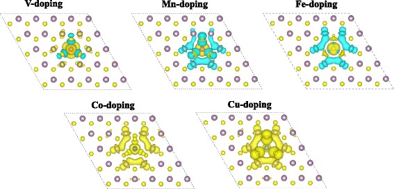
The spin-resolved charge density isosurface (isosurface value at 0.002 e/Å3) of TM-doped MoS2 monolayer at 4 % impurity concentration. Yellow and blue colors represent the spin-up and spin-down charges, respectively
In the last part, we have studied TM doping at 4 % impurity concentration by calculating one TM atom replacing one Mo atom in a 5 × 5 × 1 supercell, in which the distance between the dopants is around 16 Å. We further calculated two TM atoms replacing two Mo atoms in a 5 × 5 × 1 surpercell to investigate the TM doping at 8 % impurity concentration. There configurations with different TM-TM separations were considered: NN configurations in which the two TM atoms are in the nearest neighboring position with TM-TM distance of 3.2 Å, the second NN configurations in which the two TM atoms are in the next nearest-neighboring position with TM-TM distance of 5.5 Å, and the third NN configuration in which the distance between the two doped TM atoms are 6.5 Å.
Figure 5 summarized our calculated results on the energy differences between the FM and AFM states for the three configurations of NN, second NN, and third NN. For the four elements of V, Mn, Fe, and Co doping, the energy differences between the FM and AFM states are negative for all the three configurations, which means the FM states are more favorable energetically. Our results on the NN configuration for Mn, Fe, and Co doping agree with previous result [31, 33, 39], and our results on the third configuration agree with Ref [37]. As for Cu doping, the FM states are more favorable for the NN configurations, but for the second NN and third NN configurations, the AFM states are more stable. Table 1 lists the calculated total magnetic moments of the doped system and the local magnetic moments on the impurities for the ground states of the three configurations, and the spin-resolved charge density for the ground states is shown in Fig. 6.
Fig. 5.
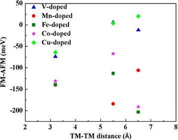
Energy differences of the FM ordering over AFM ordering for V-, Mn-, Fe-, Co-, and Cu-doped MoS2 as a function of the distance between the two doped TM atoms. The corresponding impurity concentration is 8 %
Table 1.
The magnetic moments (Σμi/μtotal) for V-, Mn-, Fe-, Co-, and Cu-doped MoS2 with impurity concentration at 4, 8, and 12 %
| 4 % | 8 % | 12 % | |||
|---|---|---|---|---|---|
| NN | 2nd NN | 3rd NN | NN | ||
| V | 0.9/1.0 | 2.2/2.0 | 1.9/0.0 | 1.8/2.0 | 3.6/3.0 |
| Mn | 2.9/1.0 | 5.8/2.0 | 5.8/2.0 | 6.4/2.0 | 6.3/5.0 |
| Fe | 3.4/2.0 | 3.6/2.0 | 4.4/4.0 | 6.4/4.0 | 7.3/2.0 |
| Co | 1.1/3.0 | 3.0/4.0 | 4.6/6.0 | 4.3/6.0 | 0.8/1.0 |
| Cu | 0.5/4.9 | 0.5/3.6 | 0.6/0.2 | 0.5/0.0 | 0.6/3.0 |
Both the local magnetic moments of the doped atoms (Σμi) and the total magnetic moments of the doped system (μtotal) are presented. Three configurations with different TM-TM distances were listed for 8 % impurity concentration
Fig. 6.
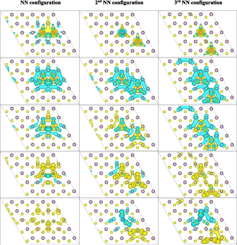
The spin-resolved charge density isosurface (isosurface value at 0.002 e/Å3) of TM-doped MoS2 monolayer at 8 % impurity concentration. The first, second, third, fourth, and fifth rows are the results for V-, Mn-, Fe-, Co-, and Cu-doped systems, respectively. And the first, second, and third columns correspond to the NN, second NN, and third NN configurations. Yellow and blue colors represent the spin-up and spin-down charges, respectively
As shown in Fig. 6, the spins of the two nearest neighbored dopants are parallel to each other for all the five doped systems. For V, Mn, and Fe doping, the induced spins on the nearby S and Mo atoms are antiparallel to that of the dopants. Thus, the total magnetic moments of the V-, Mn-, and Fe-doped system are smaller than the local magnetic moments on the dopants. As for Co and Cu doping, the total magnetic moments of the doped system are much larger than the local magnetic moments of the impurities because the spin polarizations on the nearby S and Mo atoms are all parallel to that of the dopants. Particularly, the total magnetic moment of the Cu-doped MoS2 in NN configuration at impurity concentration of 8 % is 3.6 μB although the local magnetic moments on the two Cu atoms are only 0.5 μB.
Figure 6 also shows that for V, Mn, Fe, and Co doping in the second NN and third NN configurations, the two dopants are FM coupling or even weakly AFM coupling (the energy difference between the FM and AFM states is 6 meV for V doping in the second configuration). This is similar with the NN configuration. Additionally, the magnetic orderings among the dopants and the nearby host atoms in second and third NN configuration for the four elements are similar with the situation in the NN configuration. In detail, the induced spins on the nearby S and Mo atoms are antiparallel to the impurities for V, Mn, and Fe doping, which leads to the smaller total magnetic moment relative to the local magnetic moments on the dopants, while the FM coupling between the doped Co atoms and the nearby S and Mo atoms makes the total magnetic moment larger than the local ones on the dopants. Moreover, the local magnetic moments of the Fe and Co dopants in second and third NN configurations are larger than those in the NN configuration; thus, the total magnetic moments of second and third NN configurations are larger than those in the NN configuration. For Cu doping in the second and third NN configurations, the AFM states are energetically more stable than the FM states; this is differing from the NN configuration. Figure 6 shows the AFM coupling between the two doped Cu atoms with large separations and the FM exchange with the nearby host S and Mo atoms like the NN configuration. Hence, the total magnetic moments for Cu doping in the second and third NN configurations are very close to 0.
According to our calculations, for the five elements except for Cu doping, the magnetic ordering between the doped atoms and host atoms in the second and third configurations is similar with those in the NN configurations. In contrast, Mishra et al. [39] predicted AFM coupling for the dopants with large separations and FM coupling for the dopants in NN configurations for Fe and Co doping. Additionally, according to Schwigenschlogal et al.’s study [37], Fe and Co doping also lead to AFM ground state in large separations. In this situation, we recalculated the NN, second and third configurations without U parameterizations. The energy differences between the FM and AFM states are summarized in Additional file 1: Figure S2. It shows that for Fe and Co doping in large separations, the AFM states are more favorable energetically, which agrees with previous results [37, 39]. More importantly, we found that the NN configurations are more favorable than the other two configurations with large separations. The total energy of the NN configuration is less than the second and third configurations by 0.2, 0.5, 0.8, 1.0, and 1.3 eV for V, Mn, Fe, Co, and Cu doping, respectively. This is consistent with Liu’s study which shows that the V atoms prefer to stay together in MoS2 monolayer.
On the basis of the study on doping at 8 % impurity concentration, we further studied the TM doping at higher impurity concentration in NN configurations. Three TM atoms replace three nearest neighboring Mo atoms in a 5 × 5 × 1 supercell; the corresponding impurity concentration is 12 %. As shown in Fig. 7, for the five elements except for Fe, the doped TM atoms are FM coupling with each other. For Fe doping, one of the three dopants is AFM coupling with the other two dopants. The reason making the spin polarization of this Fe atom (Fe1) differs from the other two Fe atoms (Fe2 and Fe3) mainly lies in atomic structure. Figure 8 shows the relaxed atomic structures for the five elements doped MoS2 monolayer at 12 % impurity concentration. As shown in Fig. 8, the Mn–S bond lengths for the three doped Mn atoms are close, which give rise to the similar spin polarization on the three Mn atoms. The respective local magnetic moments on Mn1, Mn2, and Mn3 are 2.9, 3.1 and 3.1 μB, respectively. Additionally, Fig. 8 shows that the Mn2–S2 and Mn3–S3 bond lengths are little larger than the other Mn–S bond lengths which makes the spin polarization on Mo* atom differs from the other nearby Mo atoms as shown in Fig. 7. As for Fe doping, the Fe–S bond lengths of the Fe1 atom are different from those of the Fe2 and Fe3 atoms. Particularly, the Fe1–S* bond length is larger than the Fe2–S* and Fe3–S* bond lengths, which makes the hybridization of Fe1 3d and S* 4p differs from the counterparts of Fe2 and Fe3 atoms. Consequently, spin of Fe1 is antiparallel to that of Fe2 and Fe3. More importantly, Fig. 8 shows that the atomic structures of V- and Mn-doped MoS2 maintain the original prismatic configuration, but the atomic structures of Co- and Cu-doped MoS2 deviate from the prismatic configuration, which is not good for applications in 2D materials.
Fig. 7.
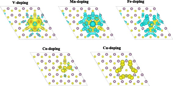
The spin-resolved charge density isosurface (isosurface value at 0.002 e/Å3) of TM-doped MoS2 monolayer at 12 % impurity concentration. Yellow and blue colors represent the spin-up and spin-down charges, respectively
Fig. 8.
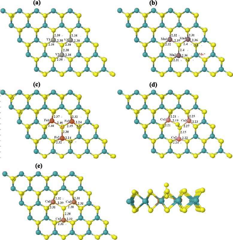
Atomic structures of TM-doped monolayer MoS2 at 12 % impurity concentration. a V doping. b Mn doping. c Fe doping. d Co doping. e Cu doping (top and side views)
Figure 7 shows that the magnetic ordering among the dopants and the nearby host atoms at 12 % impurity concentration is similar with the situation at 8 % impurity concentration; for V and Mn (Co and Cu) doping, the induced spins on the nearby host atoms are antiparallel (parallel) to those of the dopants. Thus, the total magnetic moment of V and Mn (Co and Cu) doping is less (larger) than the local magnetic moments of the three dopants. Additionally, our calculations result indicates that for V and Mn doping, the magnetic moments of the doped MoS2 increase as the increasing impurity concentration, whereas the magnetisms of Co- and Cu-doped system decrease when impurity concentration increases from 8 to 12 %.
Conclusions
Our study on MoS2 with TM doping at 4 % concentration tells us all the five 3d elements of V, Mn, Fe, Co, and Cu doping which give rise to the good diluted magnetic semiconductors. Additionally, we have found that the doped TM atoms prefer to stay in the nearest neighboring positions at high concentrations and couple with each other ferromagnetically. For V, Mn, and Fe doping, the induced spins on the nearby host atoms are antiparallel to that of the impurities, whereas for Co and Cu doping, they are parallel to that of the dopants. It indicates that the local structures around the impurities are deformed from the original prismatic configurations for Co and Cu doping at high impurity concentration although both doping induce strong ferromagnetism into the doped system. Our calculations show that, besides Mn, V is also good candidate to induce and manipulate the magnetism in 2D TMDs.
Acknowledgements
This work was supported by the National Natural Science Foundation of China (NNSFC) (21273172), the program for New Century Excellent Talents in University (NCET-13-0471). This work was also supported by the 111 Project (B08040) and the Fundamental Research Funds for the Central Universities (3102015BJ (II) JGZ005, 3102015BJ023) in China. The supports from the Beijing Computational Science Research Center and the CAEP Chengdu Science and Technology Development Center and the Chengdu Green Energy and Green Manufacturing Technology R&D Center are also appreciated.
Additional files
Supplemental information. Ferromagnetism in Transitional-Metal Doped MoS2 Monolayer. (DOC 228 kb)
Footnotes
Competing Interests
The authors declare that they have no competing interests.
Authors’ Contributions
XLF designed the study, performed the research, and drafted the manuscript. YRA and WJG participated in performing the research and helped to draft the manuscript. All authors read and approved the final manuscript.
References
- 1.Mark KF, Lee C, Hone J, Shan J, Heinz TF. Atomically thin MoS2: a new direct-gap semiconductor. Phys Rev Lett. 2010;105:136805. doi: 10.1103/PhysRevLett.105.136805. [DOI] [PubMed] [Google Scholar]
- 2.Gutiérrez HR, López NP, Elíast AL, Berkdemir A, Wang B, Lv R, Uríast FL, Crespi VH, Terronest H, Terrones M. Extraordinary room-temperature photoluminescence in triangular WS2 monolayer. Nano Lett. 2013;13:3447–3454. doi: 10.1021/nl3026357. [DOI] [PubMed] [Google Scholar]
- 3.Li Y, Wu D, Zhou Z, Cabrera CR, Chen ZJ. Enhanced Li adsorption and diffusion on MoS2 zigzag nanoribbons by edge effects: a computational study. Phys Chem Lett. 2012;3:2221–2227. doi: 10.1021/jz300792n. [DOI] [PubMed] [Google Scholar]
- 4.Fan XL, Yang Y, Xiao P, Lau WM. Site-specific catalytic activity in exfoliated MoS2 single-layer polytypes for hydrogen evolution: basal plane and edges. J Mater Chem A. 2014;2:20545–20551. doi: 10.1039/C4TA05257A. [DOI] [Google Scholar]
- 5.Fan XL, Wang SY, An YR, Lau WM. Catalytic activity of MS2 monolayer for electrochemical hydrogen evolution. J Phys Chem C. 2016;120:1623–1632. doi: 10.1021/acs.jpcc.5b10709. [DOI] [Google Scholar]
- 6.Radisavljevic B, Radenovic A, Brivio J, Giacometti V, Kis A. Single-layer MoS2 transistors. Nat Nanotechnol. 2011;6:147–150. doi: 10.1038/nnano.2010.279. [DOI] [PubMed] [Google Scholar]
- 7.Wang QH, Kalantar-Zadeh K, Kis A, Coleman JN, Strano MS. Electronics and optoelectronics of two-dimensional transitional metal dichalcogenides. Nat Nanotechnol. 2012;7:699–712. doi: 10.1038/nnano.2012.193. [DOI] [PubMed] [Google Scholar]
- 8.Cao T, Wang G, Han W, Ye H, Zhu C, Shi J, Niu Q, Tan P, Wang E, Liu B, Feng J. Valley-selective circular dichroism of monolayer molybdenum disulphide. Nat Commun. 2012;3:887. doi: 10.1038/ncomms1882. [DOI] [PMC free article] [PubMed] [Google Scholar]
- 9.Kim S, Konar A, Hwang WS, Lee JH, Lee JY, Yang JY, Jung CH, Kim HS, Yoo JB, Choi JY, Jin YW, Lee SY, Jena D, Choi W, Kim K. High-mobility and low-power thin-film transistors based on multilayer MoS2 crystals. Nat Commun. 2012;3:1011. doi: 10.1038/ncomms2018. [DOI] [PubMed] [Google Scholar]
- 10.Lembke D, Kis A. Breakdown of high-performance monolayer MoS2 transistors. ACS Nano. 2012;6:10070–10075. doi: 10.1021/nn303772b. [DOI] [PubMed] [Google Scholar]
- 11.Braga D, Gutiérrez LI, Berger H, Morpurgo AF. Quantitative determination of the band gap of WS2 with ambipolar ionic liquid-gated transistors. Nano Lett. 2012;12:5218–5223. doi: 10.1021/nl302389d. [DOI] [PubMed] [Google Scholar]
- 12.Pan H, Zhang YW. Edge-dependent structural, electronic and magnetic properties of MoS2 nanoribbons. J Mater Chem. 2012;22:7280–7290. doi: 10.1039/c2jm15906f. [DOI] [Google Scholar]
- 13.Zou X, Liu Y, Yakobson BI. Predicting dislocations and grain boundaries in two-dimensional metal-disulfides from the first principles. Nano Lett. 2012;13:253–258. doi: 10.1021/nl3040042. [DOI] [PubMed] [Google Scholar]
- 14.Cai L, He JF, Liu QH, Yao T, Chen L, Yan WS, Hu FC, Jiang Y, Zhao YS, Hu TD, Sun ZH, SQ W. Vacancy-induced ferromagnetism of MoS2 nanosheets. J Am Chem Soc. 2015;137:2622–2627. doi: 10.1021/ja5120908. [DOI] [PubMed] [Google Scholar]
- 15.Kou L, Tang C, Zhang Y, Heine T, Chen C, Frauenheim T. Tuning magnetism and electronic phase transitions by strain and electric field in zigzag MoS2 nanoribbons. J Phys Chem Lett. 2012;3:2934–2941. doi: 10.1021/jz301339e. [DOI] [PubMed] [Google Scholar]
- 16.Roldán R, Silva‐Guillén JA, López‐Sancho MP, Guinea F, Cappelluti E, Ordejón P. Electronic properties of single-layer and multilayer transition metal dichalcogenides MX2 (M = Mo, W and X = S, Se) Ann Phys. 2014;526:347–357. doi: 10.1002/andp.201400128. [DOI] [Google Scholar]
- 17.Zheng H, Yang B, Wang D, Han R, Du X, Yan Y. Tuning magnetism of monolayer MoS2 by doping vacancy and applying strain. Appl Phys Lett. 2014;104:132403. doi: 10.1063/1.4870532. [DOI] [Google Scholar]
- 18.Andriotis AN, Menon M. Tunable magnetic properties of transition metal doped MoS2. Phys Rev B. 2014;90:125304. doi: 10.1103/PhysRevB.90.125304. [DOI] [Google Scholar]
- 19.Feng N, Mi WB, Cheng YC, Guo ZB, Schwingenschlögl U, Bai HL. Magnetism by interfacial hybridization and p-type doping of MoS2 in Fe4N/MoS2 superlattices: a first-principles study. ACS Appl Mater Inter. 2014;6:4587–4594. doi: 10.1021/am500754p. [DOI] [PubMed] [Google Scholar]
- 20.Ramasubramaniam A. Mn-doped monolayer MoS2: an atomically thin dilute magnetic semiconductor. Phys Rev B. 2013;87:195201. doi: 10.1103/PhysRevB.87.195201. [DOI] [Google Scholar]
- 21.Sun QC, Mazumdar D, Yadgarov L, Rosentsveig R, Tenne T, Musfeld JL. Spectroscopic determination of phonon lifetimes in rhenium-doped MoS2 nanoparticles. Nano Lett. 2013;13:2803–2808. doi: 10.1021/nl401066e. [DOI] [PubMed] [Google Scholar]
- 22.Yun WS, Lee JD. Unexpected strong magnetism of Cu doped single-layer MoS2 and its origin. Phys Chem Chem Phys. 2014;16:8990–8996. doi: 10.1039/c4cp00247d. [DOI] [PubMed] [Google Scholar]
- 23.Feng N, Mi WB, Cheng YC, Guo ZB, Schwingenschlögl U, Bai HL. First principles prediction of the magnetic properties of Fe-×6 (X = S, C, N, O, F) doped monolayer MoS2. Sci Rep. 2014;4:3987. doi: 10.1038/srep03987. [DOI] [PMC free article] [PubMed] [Google Scholar]
- 24.Cheng YC, Zhu ZY, Mi WB, Guo ZB, Schwingenschlögl U. Prediction of two-dimensional diluted magnetic semiconductor: doped monolayer MoS2 system. Phys Rev B. 2013;87:100401. doi: 10.1103/PhysRevB.87.100401. [DOI] [Google Scholar]
- 25.Dolui K, Rungger I, Pemmaraju CD, Sanvito S. Possible doping strategies for MoS2monolayers: an ab initio study. Phys Rev B. 2013;88:075420. doi: 10.1103/PhysRevB.88.075420. [DOI] [Google Scholar]
- 26.Mishra R, Zhou W, Pennycook SJ, Pantelides ST, Idrobo JC. Long-range ferromagnetic ordering in manganese-doped two-dimensional dichalcogenides. Phys Rev B. 2013;88:144409. doi: 10.1103/PhysRevB.88.144409. [DOI] [Google Scholar]
- 27.Zhao X, Xia C, Wang T, Dai X. Electronic and magnetic properties of X-doped (X = Ti, Zr, Hf) tungsten disulphide monolayer. J Alloys Compd. 2016;654:574–579. doi: 10.1016/j.jallcom.2015.09.160. [DOI] [Google Scholar]
- 28.Lu SC, Leburton JP. Electronic structures of defect and magnetic impurities in MoS2 monolayer. Nanoscale Res Lett. 2014;9:676. doi: 10.1186/1556-276X-9-676. [DOI] [PMC free article] [PubMed] [Google Scholar]
- 29.Xiang ZC, Zhang Z, Xu XJ, Zhang Q, Wang QB, Yuan CW. Room-temperature ferromagnetism in Co doped MoS2 sheets. Phys Chem Chem Phys. 2015;17:15822. doi: 10.1039/C5CP01509J. [DOI] [PubMed] [Google Scholar]
- 30.Fuhr JD, Saul A, Sofo JO. Scanning tunneling microscopy chemical signature of point defects on the MoS2(001) surface. Phys Rev Lett. 2004;92:026802. doi: 10.1103/PhysRevLett.92.026802. [DOI] [PubMed] [Google Scholar]
- 31.He JG, Wu KC, Sa RJ, Li QH, Wei YQ. Magnetic properties of nonmetal atoms adsorbed MoS2 monolayers. Appl Phys Lett. 2010;96:082504. doi: 10.1063/1.3318254. [DOI] [Google Scholar]
- 32.Kresse G, Furthmüller J. Efficient iterative schemes for ab initio total-energy calculations using a plane-wave basis set. Phys Rev B. 1996;54:11169. doi: 10.1103/PhysRevB.54.11169. [DOI] [PubMed] [Google Scholar]
- 33.Kresse G, Joubert D. From ultrasoft pseudopotentials to the projector augmented-wave method. Phys Rev B. 1999;59:1758. doi: 10.1103/PhysRevB.59.1758. [DOI] [Google Scholar]
- 34.Blöchl PE. Projector augmented-wave Method. Phys Rev B. 1994;50:17953. doi: 10.1103/PhysRevB.50.17953. [DOI] [PubMed] [Google Scholar]
- 35.Perdew JP, Burke K, Ernzerhof M. Generalized gradient approximation made simple. Phys Rev Lett. 1996;77:3865. doi: 10.1103/PhysRevLett.77.3865. [DOI] [PubMed] [Google Scholar]
- 36.Chanier T, Sargolzaei M, Opahle I, Hayn F, Koepernik K. Electronic and magnetic properties of V-doped anatase TiO2 from first principles. Phys Rev B. 2006;73:134418. doi: 10.1103/PhysRevB.73.134418. [DOI] [Google Scholar]
- 37.Monkhorst HJ, Pack JD. Special points for Brillouin-zone integrations. Phys Rev B. 1976;13:5188. doi: 10.1103/PhysRevB.13.5188. [DOI] [Google Scholar]
- 38.Yazyev OV. Emergence of magnetism in graphene materials and nanostructures. Rep Prog Phys. 2010;73:056501. doi: 10.1088/0034-4885/73/5/056501. [DOI] [Google Scholar]
- 39.Yang JH, Kim DY, Hong JS, Qian XH. Magnetism in boron nitride monolayers: adatom and vacancy defects. Surf Sci. 2010;604:1603–1607. doi: 10.1016/j.susc.2010.06.001. [DOI] [Google Scholar]
- 40.Zhou YG, Yang P, Zu HY, Gao F, Zu XT. Electronic structures and magnetic properties of MoS2 nanostructures: atomic defects, nanoholes, nanodots and antidots. Phys Chem Chem Phys. 2013;15:10385–10394. doi: 10.1039/c3cp50381j. [DOI] [PubMed] [Google Scholar]
- 41.Sun XT, Wang L, Lin HP, Li YY. Induce magnetism into silicone by embedding transition-metal atoms. Appl Phys Lett. 2015;106:222401. doi: 10.1063/1.4921699. [DOI] [Google Scholar]
- 42.Gao JF, Zhang JF, Liu HS, Zhang QF, Zhao JJ. Structures, motilities, electronic and magnetic properties of point defects in silicene. Nanoscale Res Lett. 2013;5:9785. doi: 10.1039/c3nr02826g. [DOI] [PubMed] [Google Scholar]


