Abstract
Few-layer black phosphorus (BP) is the most promising material among the two-dimensional materials due to its layered structure and the excellent semiconductor properties. Currently, thin BP atomic layers are obtained mostly by mechanical exfoliation of bulk BP, which limits applications in thin-film based electronics due to a scaling process. Here we report highly crystalline few-layer black phosphorus thin films produced by liquid exfoliation. We demonstrate that the liquid-exfoliated BP forms a triangular crystalline structure on SiO2/Si (001) and amorphous carbon. The highly crystalline BP layers are faceted with a preferred orientation of the (010) plane on the sharp edge, which is an energetically most favorable facet according to the density functional theory calculations. Our results can be useful in understanding the triangular BP structure for large-area applications in electronic devices using two-dimensional materials. The sensitivity and selectivity of liquid-exfoliated BP to gas vapor demonstrate great potential for practical applications as sensors.
The increasing demand for elemental 2D materials, such as graphene and transition metal dichalcogenides (TMDCs), emerged for applications in sensors1,2,3, optoelectronics4,5, flexible displays6, and photovoltaics7,8. Although graphene has high carrier mobility9, its zero band gap limits various electronic applications10. Recent studies found that phosphorene, monolayer of black phosphorus, can be mechanically exfoliated similarly to graphene10,11,12,13,14. Contrary to graphene, black phosphorus (BP) has a band gap of 0.3–2 eV, which allows it to be exploited as an excellent semiconductor and potentially an alternative for graphene7,10,15,16,17,18. In addition, we reported that BP can be applied to produce highly efficient photocatalyst19,20.
Previous studies on the electronic applications of BP21,22 are based on the layer-dependent nature of BP23,24. Bulk BP layers are stacked together by the van der Waals force and can be easily peeled off layer by layer25. Most of the recent studies on BP are based on mechanically exfoliated BP bulk samples24. Although mechanical exfoliation is an effective technique to cleave bulk materials into mono or few layers, it is limited by a scaling process. Therefore, it is necessary to employ a liquid method for large scale and various practical applications.
Previous work proved that BP deposited on SiO2/Si by the liquid exfoliation forms high-quality single crystalline nanoflakes26. Brent et al. reported that few-layer phosphorene was produced by liquid exfoliation of BP in N-methyl-2-pyrrolidone27. Other studies on BP layers by liquid exfoliation showed that BP atomic layers look like debris or flakes with a random shape or orientation28,29,30. None of them, however, showed well-defined crystalline thin films covering whole substrates. Hence, they appear to be inappropriate for thin-film based electronic applications.
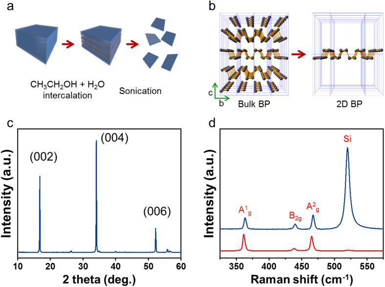
Our liquid exfoliation method uses higher sonication energies than the conventional method and different solutions, as illustrated in Fig. 1a, which allows us to obtain highly crystalline triangle-shaped BP thin films. Unlike the liquid-exfoliated BP flakes with random shapes reported in the literature, our BP sample cleaves into faceted triangular atomic layers, similar to triangle-shaped flakes commonly observed in MoS2 nanocrystals31,32,33,34. The thickness and the density of BP layers on the substrate can be easily changed by adjusting the sonic energy and the concentration of BP in our sample. Using our method, it is possible to produce ultrathin BP films varying in thickness from monolayers to few layers. It can be challenging to design uniform thin films using BP flakes with random shapes because high coverage of BP is needed to uniformly cover the whole substrate, which results in thick stacked BP layers close to bulk BP. The fabrication of nano devices using single BP flakes has been demonstrated in the literature35,36,37, which is not suitable for large-area processing. On the other hand, triangular BP layers can effectively cover the whole substrate with low coverage, which facilitates the fabrication of uniform thin films. This makes the liquid-exfoliated BP a perfect candidate for large-area applications in electronic devices.
Figure 1.
(a) Schematic illustration of liquid exfoliation procedure of BP using high energy ultrasonic irradiation (b) The corresponding atomic modelling depicting bulk BP cleaved into monolayer BP. (c) XRD pattern of liquid-exfoliated BP indicating the crystalline phase of BP. (d) Raman spectra of liquid-exfoliated BP. Inset: three types of optical phonon modes of BP depicting A1g at 363 cm−1, B2g at 440 cm−1 and A2g at 467 cm−1.
In this study, we used ultrasonic energy (Fig. 1b) to exfoliate bulk BP, breaking it down into mono or few layers, and investigated the surface properties of liquid-exfoliated BP multilayers on SiO2/Si (001) substrates using atomic force microscopy (AFM), scanning electron microscopy (SEM), transmission electron microscopy (TEM), Raman spectroscopy, and X-ray diffractometer (XRD) in combination with density functional theory (DFT) calculations. We found that the liquid-exfoliated BP forms a layer-by-layer structure with well-defined triangle-shaped crystals. In addition, the practical applications of liquid-exfoliated BP as chemical sensors were explored using field-effect transistors (FETs) and diode devices.
Results
Crystal structure of BP
The XRD measurements were carried out to examine the crystal structure of BP samples produced by liquid exfoliation. As shown in Fig. 1c, sharp and strong peaks were observed at 2θ = 16.89° for the (002) plane, 34.17° for the (004) plane and 52.32° for the (006) crystal plane. Based on the XRD data, we found that our BP samples have an orthorhombic structure with lattice constants of a = 3.32 Å, b = 4.38 Å and c = 10.48 Å, which agrees with the previous studies for BP38.
Raman spectroscopy measurements were performed to verify the crystalline structure of liquid-exfoliated BP. BP flakes were obtained from a droplet of the liquid- exfoliated BP on SiO2/Si (001). The sample was dried to remove the solvent. Figure 1d shows the Raman spectra measured at two different positions within a single BP flake. In the spectra, there are four prominent peaks at 363 cm−1, 440 cm−1, 467 cm−1 and 520 cm−1. The BP flake is thin enough to observe the Si peak at 520 cm−1 [ref. 39]. The peaks at 363 cm−1, 440 cm−1 and 467 cm−1 are known to result from the optical phonons of a crystalline lattice of BP40. They match the Raman shifts attributed to one out-of-plane vibration mode (A1g) at 363 cm−1 and two in-plane vibration modes (B2g and A2g) at 440 cm−1 and 467 cm−1. As shown in the inset of Fig. 1d, BP atoms vibrate along the c axis represented as A1g and along the b axis indicated as A2g. The model for B2g illustrates the in-plane vibration mode of BP atoms. The peak for each vibration mode of our BP sample deviates from that of bulk BP in the literature: 365 cm−1 for A1g, 442 cm−1 for B2g, and 470 cm−1 for A2g39. Instead, the positions of these peaks are consistent with the Raman shift values of BP multilayers by Lu et al.41, which implies that BP prepared by liquid exfoliation exhibits the crystalline thin-film phase.
Surface topography of BP
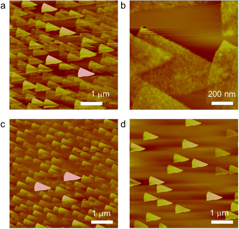
The surface morphology of BP was investigated using AFM. The repeatable measurements from a number of BP samples demonstrate that BP forms triangle-shaped atomic layers on SiO2/Si (001). As shown in Fig. 2, the triangular BP layers are faceted, which proves that the BP layers are single crystalline. The different contrast in the images indicates that BP forms a layered structure on SiO2/Si (001), as shown in Fig. 2a. The height of the triangular BP crystal in Fig. 2b is approximately 1 nm. A series of height measurements revealed that the triangular BP crystals in Fig. 2a have three different thicknesses: 1.10 ± 0.16 nm, 1.71 ± 0.12 nm and 2.50 ± 0.2 nm. The height data indicate that there are at least two BP atomic layers in each 1 nm-high triangle and roughly 4–8 atomic layers stacked on the higher triangles. The average lateral size of the triangular BP crystals is approximately 756 ± 25 nm. We also experimented with various conditions such as different sonication time and different spin coating rpm. In varying the sonication time from 5 min. to 40 min., we found that a change in the sonication time resulted in a change in the concentration of BP in the solution, which leads to a change in the size, density, and thickness of BP crystals. The thinnest BP layer we observed was about 3 Å in height.
Figure 2. Structure of liquid-exfoliated BP demonstrating single crystalline thin film phase.
(a) AFM image of triangle-shaped BP layers formed on SiO2/Si (001) spin-coated at 2500 rpm (5 μm × 5 μm), (b) Enlarged AFM image of BP layers (790 nm × 790 nm) (c) Degradation of BP thin film with lower concentration (5 μm × 5 μm). (d) Degradation of BP thin film with higher concentration (5 μm × 5 μm).
Figure 2c,d show the AFM images of liquid-exfoliated BP samples with two different concentrations. The concentration of the BP sample in Fig. 2d is higher than that of Fig. 2c. The biggest difference is that the number of thicker BP islands (>8 nm high) is larger in Fig. 2d. This means the higher BP concentration results in the larger density of higher triangles. The AFM image in Fig. 2c shows that the bottom part of each triangular crystal is not as clear as the top part because the BP thin film started to degrade (see Supplementary Fig. S2). The reason why the number of triangular BP crystals is less in Fig. 2d is that the AFM image was taken a few days after the sample was prepared. The thin BP islands (~1 nm high) were gone by that time and only thick BP crystals were survived.
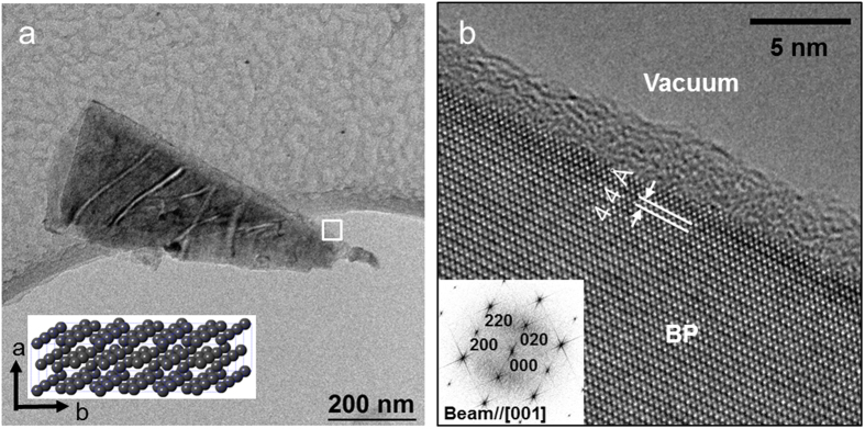
The formation of triangular BP layers is a characteristic feature of a BP crystal regardless of the substrates. Figure 3a shows a bright-field TEM image of BP produced by liquid-exfoliation formed on an amorphous carbon grid. The TEM image shows a BP flake formed in a triangular shape, which coincides with the AFM image. This morphological feature allows easy identification of the crystal orientation. The size of the crystal is approximately 800 nm, which is consistent with the size of the BP triangle in the AFM image. The atomic-scale image in Fig. 3b shows the lattice structure of BP from the straight edge of the triangular BP crystal marked as a rectangular box in Fig. 3a and the corresponding fast Fourier transform (FFT) pattern. The interlayer distance measured from the high-resolution TEM image was approximately 4.4 Å along the b-axis of the unit cell. This interlayer distance is very close to the lattice constant b = 4.38 Å measured from the XRD pattern. The comparison between the atomic model in the inset in Fig. 3a and the FFT pattern in Fig. 3b suggests that the straight edge of the triangular BP crystal is assigned to the (010) plane. The only difference between TEM and AFM results is that the BP flake in the TEM image is thicker than those of AFM images. Thin BP flakes degraded fast due to the incident electron beam during the TEM measurements.
Figure 3.
(a) Bright-field TEM image of liquid exfoliated BP on a quantifoil grid. Inset: BP atomic model (b) High-resolution TEM image at atomic scale. Inset: fast Fourier transform.
We also carried out SEM measurements in order to verify the observations from AFM. Similar to the TEM experiment, thin BP layers were hard to image during the SEM measurements because of the electron beam damage or a contamination problem (see Supplementary Fig. S2).
Practical Applications as Sensors
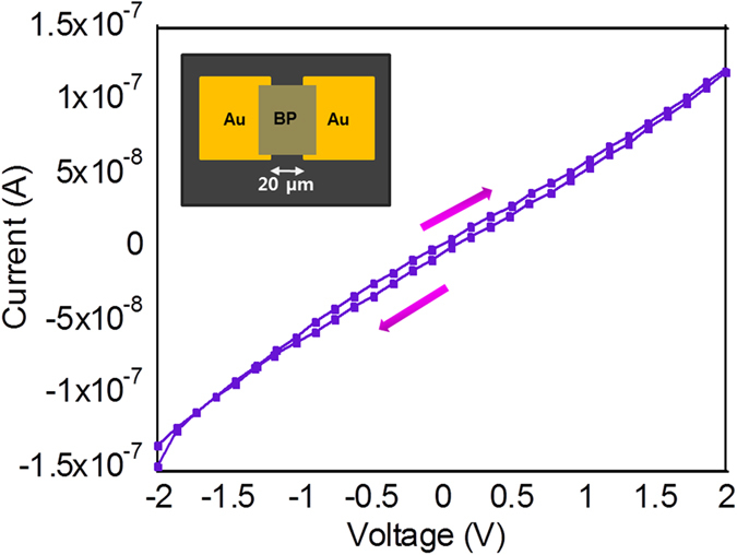
The carrier transport properties of liquid exfoliated BP were examined using a bottom-contact FET. The liquid-exfoliated BP was drop-casted on an FET where the source and the drain electrodes are pre-patterned onto the SiO2 gate dielectric substrate. The inset in Fig. 4 shows the structure of a BP FET with the channel length of 20 μm. Our results revealed that the drain current modulation induced by the gate electric field was not observed (see Supplementary Fig. S4a), which is attributed to the degradation of the FET device resulted from surface defects, oxidation and interface charge traps42 since ultrathin BP FETs are more sensitive to interface states than bulk BP. Instead the current-voltage (I–V) response of the BP FET was obtained as shown in Fig. 4. The arrows indicate the sweeping directions. The voltage was swept from −2 V to 2 V and the measured current was in the order of 10−7 A.
Figure 4. Current-voltage characteristic curve of liquid- exfoliated BP drop-casted on an FET with a channel length of 20 μm.
We tested if liquid-exfoliated BP can be applied in other electrical devices. The sensitivity of BP to the surrounding atmosphere can be applied as vapor sensors. Previous study reported that gas molecule adsorption led to change in the charge transport in phosphorene, which implies that phosphorene can be used as superior gas sensors43. We fabricated liquid-exfoliated BP sensors and examined the current as a function of time before and after the exposure to acetone (C3H6O). Acetone is a highly flammable toxic chemical widely used to dissolve substances, to make plastics, and to clean products. We found that the current was increased by two orders of magnitude after the device was exposed to acetone (see Supplementary Fig. S4b). This implies that liquid-exfoliated BP selectively detects acetone vapor and the sensing capability of BP can be used for practical applications.
Theoretical calculations
We performed DFT calculations to investigate the energetically preferred edge of the BP layer. Figure 5 shows the atomic structure of BP monolayer, and the black dotted box represents the unit cell. Using one-dimensional BP nanoribbons where the atomic layer is cut along the different lines as shown in Fig. 5, the formation energy of the edges was calculated as follows
Figure 5. Atomic structure of BP monolayer calculated by DFT.
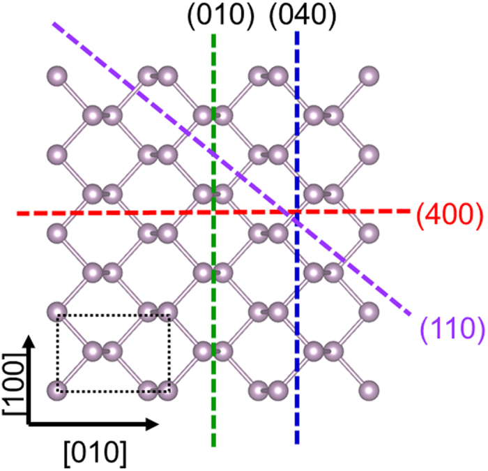
The green, blue, purple and red dashed lines represent (010), (040), (400) and (110) planes, respectively. The figure was generated by the VESTA software.
 |
where Etot[edge] is the total energy of the edge system, np is the number and μp is the chemical potential of phosphorus atoms. The factor 1/2 represents two equivalent edges in the nanoribbon. μp was calculated from the total energy of the pristine BP monolayer. The formation energies per unit cell for the (400) and (040) edges are the same as 1.24 eV (see Supplementary Table S1). On the contrary, the formation energy per unit cell for the (010) edge is 0.69 eV. Similarly, the formation energies per unit length for the (040), (400), (110) and (010) edges are 0.37, 0.27, 0.34 and 0.21 eV/Å, respectively, which indicates that the (010) edge is energetically most stable.
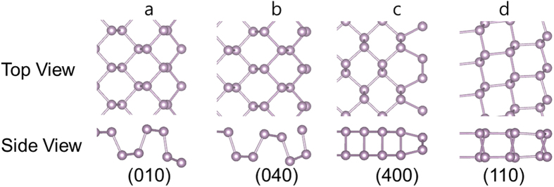
Figure 6 depicts the atomic model of the top view and the side view of the BP monolayer in DFT calculations. All the edges undergo significant lattice relaxations, except the (110) edge. The edge reconstructions result in a decrease in the energy of the edges by lowering or self-passivating dangling bond levels. We calculated the formation energy of the (110) edges and found that the (110) edge also has higher energy density than the (010) edge (see Supplementary Table S1). While the (040) and (400) edges have two dangling bonds per unit cell, the (010) edge has only one dangling bond, which explains why the (010) edge has the lowest energy. Our first-principle calculations show that the (010) edge is the most stable structure. Comparison between the AFM and TEM images, as well as the calculations, suggests that the straight edge of each triangular BP layer is formed along the (010) plane because it is an energetically preferred facet.
Figure 6. Top and side views of atomic structure of BP monolayer calculated by DFT.
(a) (010) plane, (b) (040) plane, (400) plane and (d) (110) plane.
Discussion
Our XRD and Raman data clearly indicate that the liquid-exfoliated BP has a single crystalline phase. The AFM results show that it is possible to fabricate BP thin films with triangle-shaped crystals in various thicknesses from monolayers to multilayers of BP. In the AFM images of BP in Fig. 2, notice that the lower side of each triangle is curved while the upper side is straight, which presumably might reflect different edge reconstructions15. Previous study of DFT calculations on BP predicted that 2D phosphorene has two edge states: armchair and zigzag15. Our ongoing work to differentiate armchair edges from zigzag edges in the triangular BP layer is in progress.
The AFM results show that the liquid-exfoliated BP samples degrade with time as shown in Fig. 2 and Fig. S2 (see Supplementary Fig. S2). The reason why there are no thin BP layers observed in Fig. 2d is that over time thinner BP layers disappear faster than thicker layers. Previous studies reported that BP atomic layers degrade in ambient air, which arises from surface reactions with ambient gas molecules. In addition, the degradation of BP is ascribed to surface defects, oxidation and interface trap states42. The degradation process of BP has never been observed in real-space images. According to the AFM images, the bottom part of each triangular BP crystal disappears first, and the straight edge part degrades more slowly (see Supplementary Fig. S2). We assume that the smearing phenomenon may result from different edge reconstructions of a BP island, and the bottom part of each island may have an atomic structure that breaks up easily in ambient air23. There might be more defects leading to surface oxidation in the bottom part of the triangular BP crystals. Atomic-scale study is required to examine the edge terminations.
The structure of liquid-exfoliated BP was examined based on the surface topography in combination with DFT calculations. Our results demonstrated that BP produced by the liquid exfoliation forms triangular crystalline structure on SiO2/Si (001) as well as amorphous carbon substrates. The triangular BP crystals are faceted with the preferred orientation of (010) plane, which suggests that liquid-exfoliated BP forms a well-defined thin-film phase on the substrates. In addition, varying the concentration of BP in the solution can change the size, thickness, and density of the BP crystals.
Our findings show that simple fabrication for large area processing and the layer-by-layer structure of highly crystalline BP films allow for integration into electronic devices. Particularly, BP can be optimized for applications in chemical sensors since the layer-by-layer structure of the BP layer induces uniform reaction sites. Indeed, our chemical BP sensors demonstrated that the highly crystalline faceted structure of BP layers has great potential for high selectivity and sensitivity of chemical vapor (see Supplementary Figs S4 and S5). Furthermore, facile processing conditions into hetero-structured thin films provide flexibility in designing functional interfaces requiring efficient charge transfer, which enables applications as photovoltaic and hydrogen producing devices.
Methods
Experimental
Structural studies of the BP on SiO2/Si (001) were performed using AFM (Digital Instruments: Nanoscope Multimode IV). The AFM measurements were carried out in four different areas of each sample with different scan sizes from 1 μm to 15 μm. Antimony-doped n-type Si (001) with 0.008–0.02 Ω·cm resistivity was used as a substrate and cleaned using the interuniversity microelectronics center (IMEC) process44. The bulk BP was cleaved and chemically exfoliated into few atomic layers of BP in an appropriate solution. Figure 1(a) depicts the liquid-exfoliation procedure of BP. The 0.2 g of BP 6.4 mmol was dispersed in a 200 mL of deionized water (100 ml)/anhydrous ethyl alcohol (100 ml) solution by high-energy ultrasonic irradiation for 20 min. to form few layers of BP. The dispersion of BP layers was performed using high-energy ultrasound at 20 kHz applied from the top of a polypropylene bottle reactor (500 mL) using a Sonics and Materials VC750 ultrasonic generator. The electrical energy input was maintained at 100 W. As shown in Fig. 1b, once bulk BP is cleaved into monolayers, a phosphorus atom is covalently bonded with three neighboring phosphorus atoms to form a puckered Honeycomb structure in a 2D sheet25,45. The crystalline structure of BP was investigated using XRD (Rigaku RDA-cA X-ray diffractometer) patterns obtained using Cu Kα radiation through a nickel filter. Raman spectroscopy was also performed (Renishaw, RM1000-Invia) in a backscattering configuration excited with a visible laser light (wavelength = 514 nm), a notch filter cut-off frequency of 50 cm−1, and a focus spot size of 5 μm. Spectra were collected through a 100× objective and recorded with 1800 lines mm−1 grating providing the spectral resolution of ~1 cm−1. To avoid laser-induced heating and ablation of the samples, all spectra were recorded at low power levels P ~ 0.1 mW and short integration times (~5 s). For structural analysis using AFM, liquid-exfoliated BP in a solution was spin-coated at 2500 rpm for 30 s twice and baked in an oven overnight. For TEM measurements, the BP sample was dispersed on a qantifoil TEM grid and dried thoroughly. Then the measurements were carried out using a Libra 200 energy-filtered TEM with an aberration corrector (Carl Zeiss). For SEM measurements, spin coated BP on a Si substrate was investigated by means of MERLIN (Carl Zeiss), with the accelerating voltage ranging from 100 eV to 1 kV for BP films. A bottom-contact FET was fabricated in which source and drain electrodes (Au/Ti) were patterned on a 200 nm thick SiO2 gate dielectric using photolithography. Highly doped p-type silicon was used as a gate electrode. BP thin films were drop-casted from a solution and dried at 90 °C in air. All the electrical measurements were carried out in air.
Theoretical
Our calculations are based on DFT with the Perdew-Burke-Ernzerhof exchange-correlation functional46, as implemented in the VASP code47. Projector augmented wave potentials are used to represent ion cores48. Wave functions are in a plane-wave basis with an energy cut-off of 400 eV. Optimized lattice constants were used, and all atoms were fully relaxed until the residual forces are less than 0.01 eV/Å. The Brillouin zone is sampled by k-point meshes equivalent to the 15 × 11 Monkhorst-Pack mesh for a (1 × 1) cell. BP is separated from its periodic images by 12 Å vacuum regions.
Additional Information
How to cite this article: Seo, S. et al. Triangular Black Phosphorus Atomic Layers by Liquid Exfoliation. Sci. Rep. 6, 23736; doi: 10.1038/srep23736 (2016).
Supplementary Material
Acknowledgments
This research was supported by the Korean Basic Science Institute research Grant No. E36800.
Footnotes
Author Contributions S.S., H.U.L. and J.L. designed the project and organized the entire research. S.S. and H.K. carried out the AFM measurements and data analysis. H.U.L. and S.C.L. performed the chemical exfoliation of B.P. and Y.K. measured the Raman spectra. J.B. did the DFT calculations. J.W. performed the TEM measurements and structure analysis. Y.K. and Professor B.P. performed the electrical measurements for practical applications. J.L. also coordinated and supervised the entire project.
References
- Perkins F. K. et al. Chemical vapor sensing with monolayer MoS2. Nano Lett. 13, 668–673 (2013). [DOI] [PubMed] [Google Scholar]
- Kumar B. et al. The role of external defects in chemical sensing of graphene field effect transistors. Nano Lett. 13, 1962–1968 (2013). [DOI] [PubMed] [Google Scholar]
- Shao Y. et al. Graphene based electrochemical sensors and biosensors: a review. Electroanalysis 22, 1027–1036 (2010). [Google Scholar]
- Lopez-Sanchez O., Lembke D., Kayci M., Radenovic A. & Kis A. Ultrasensitive photodetectors based on monolayer MoS2. Nat. Nanotechnol. 8, 497–501 (2013). [DOI] [PubMed] [Google Scholar]
- Kuc A., Zibouche N. & Heine T. Influence of quantum confinement on the electronic structure of the transition metal sulfide TS2. Phys. Rev. B 83, 245213 (2011). [Google Scholar]
- Kim K. S. et al. Large-scale pattern growth of graphene films for stretchable transparent electrodes. Nature 457, 706–710 (2009). [DOI] [PubMed] [Google Scholar]
- Buscema M. et al. Fast and broadband photoresponse of few-layer black phosphorus field-effect transistors. Nano Lett. 14, 3347–3352 (2014). [DOI] [PubMed] [Google Scholar]
- Deng Y. et al. Black phosphorus-Monolayer MoS2 van der Waals heterojunction p-n diode. ACS Nano 8, 8292–8299 (2014). [DOI] [PubMed] [Google Scholar]
- Heyd J., Scuseria G. E. & Ernzerhof M. Hybrid functional based on a screened Coulomb potential. J. Chem. Phys. 118, 8207–8215 (2003). [Google Scholar]
- Liu H. et al. Phosphorene: An unexplored 2D semiconductor with a high hole mobility. ACS Nano 8, 4033–4041 (2014). [DOI] [PubMed] [Google Scholar]
- Xia F., Wang H. & Jia Y. Rediscovering black phosphorus as an anisotropic layered material for optoelectronics and electronics. Nat. Commun. 5, 4458 (2014). [DOI] [PubMed] [Google Scholar]
- Das S. et al. Tunable transport gap in phosphorene. Nano Lett. 14, 5733–5739 (2014). [DOI] [PubMed] [Google Scholar]
- Koenig S. P., Doganov R. A., Schmidt H., Castro Neto A. H. & Özyilmaz B. Electric field effect in ultrathin black phosphorus. Appl. Phys. Lett. 104, 103106 (2014). [Google Scholar]
- Castellanos-Gomez A. et al. Isolation and characterization of few-layer black phosphorus. 2D Mater. 1, 025001 (2014). [Google Scholar]
- Liang L. et al. Electronic bandgap and edge reconstruction in phosphorene materials. Nano Lett. 14, 6400–6406 (2014). [DOI] [PubMed] [Google Scholar]
- Tran V., Soklaski R., Liang Y. & Yang L. Layer-controlled band gap and anisotropic excitons in few-layer black phosphorus. Phys. Rev. B 89, 235319 (2014). [Google Scholar]
- Cai Y., Zhang G. & Zhang Y.–W. Layer-dependent band alignment and work function of few-layer phosphorene. Sci. Rep. 4, 6677 (2014). [DOI] [PMC free article] [PubMed] [Google Scholar]
- Guan J., Zhu Z. & Tománek D. Phase coexistence and metal-insulator transition in few-layer phosphorene: a computational study. Phys. Rev. Lett. 113, 046804 (2014). [DOI] [PubMed] [Google Scholar]
- Lee H. et al. Stable semiconductor black phosphorus (BP) @ titanium dioxide (TiO2) hybrid photocatalysts. Sci. Rep. 5, 8691 (2015). [DOI] [PMC free article] [PubMed] [Google Scholar]
- Lee H. et al. Black phosphorus (BP) nanodots for potential biomedical applications. Small 12, 214–219 (2015). [DOI] [PubMed] [Google Scholar]
- Sun J. et al. Formation of stable phosphorus-carbon bond for enhanced performance in black phosphorus nanoparticle-graphite composite battery anodes. Nano Lett. 14, 4573–4580 (2014). [DOI] [PubMed] [Google Scholar]
- Sun L.–Q. et al. Electrochemical activity of black phosphorus as an anode material for lithium-ion batteries. J. phys. Chem. C 116, 14772–14779 (2012). [Google Scholar]
- Buscema M., Groenendijk D. J., Steele G. A., van der Zant H. S. J. & Castellanos-Gomez A. Photovoltaic effect in few-layer black phosphorus PN junctions defined by local electrostatic gating. Nat. Commun. 5, 4651 (2014). [DOI] [PubMed] [Google Scholar]
- Li L. et al. Black phosphorus field-effect transistors. Nat. Nanotechnol. 9, 372–377 (2014). [DOI] [PubMed] [Google Scholar]
- Appalakondaiah A., Vaitheeswaran G., Lebègue S., Christensen N. E. & Svane A. Effect of van der Waals interactions on the structural and elastic properties of black phosphorus. Phys. Rev. B 86, 035105 (2012). [Google Scholar]
- Yasaei P. et al. High-quality black phosphorus atomic layers by liquid-phase exfoliation. Adv. Mater. 27, 1887–1892 (2015). [DOI] [PubMed] [Google Scholar]
- Brent R. et al. Production of few-layer phosphorene by liquid exfoliation of black phosphorus. Chem. Commun. 50, 13338–13341 (2014). [DOI] [PubMed] [Google Scholar]
- Kang J. et al. Solvent exfoliation of electronic-grade, two-dimensional black phosphorus. ACS Nano 9, 3596–3604 (2015). [DOI] [PubMed] [Google Scholar]
- Lu S. B. et al. Broadband nonlinear optical resonance in multi-layer black phosphorus: an emerging infrared and mid-infrared optical material, Optics Express 23, 11183–11194 (2015). [DOI] [PubMed] [Google Scholar]
- Hanlon D. et al. Liquid exfoliation of solvent-stabilized few-layer black phosphorus for applications beyond electronics. Nat. Commun. 6, 8563 (2015). [DOI] [PMC free article] [PubMed] [Google Scholar]
- Helveg S. et al. Atomic-scale structure of single-layer MoS2 nanoclusters. Phys. Rev. Lett. 84, 951–954 (2000). [DOI] [PubMed] [Google Scholar]
- Yin X. et al. Edge nonlinear optics on a MoS2 atomic monolayer. Science 344, 488–490 (2014). [DOI] [PubMed] [Google Scholar]
- Van der Zande A. M. et al. Grains and grain boundaries in highly crystalline monolayer molybdenum disulphide. Nat. Mater. 12, 554–561 (2013). [DOI] [PubMed] [Google Scholar]
- Duan X. et al. Lateral epitaxial growth of two-dimensional layered semiconductor heterojunctions. Nat. Nanotechnol. 9, 1024–1030 (2014). [DOI] [PubMed] [Google Scholar]
- Doganov R. A. et al. Transport properties of pristine few-layer black phosphorus by van der Waals passivation in an inert atmosphere. Nat. Commun. 6, 6647 (2015). [DOI] [PubMed] [Google Scholar]
- Cui S. et al. Ultrahigh sensitivity and layer and layer-dependent sensing performance of phosphorene-based gas sensors. Nat. Commun. 6, 8632 (2015). [DOI] [PMC free article] [PubMed] [Google Scholar]
- Viti L. et al. Black phosphorus terahertz photodetectors. Adv. Mater. 27, 5567–5572 (2015). [DOI] [PubMed] [Google Scholar]
- Carts L., Srinivasa S. R., Riedner R. J., Jorgensen J. D. & Worlton T. G. Effect of pressure on bonding in black phosphorus. J. chem. Phys. 71, 1718–1721 (1979). [Google Scholar]
- Chen H. et al. Crosshatching on a SiGe film grown on a Si (001) substrate studied by Raman mapping and atomic force microscopy. Phys. Rev. B 65, 233303 (2002). [Google Scholar]
- Koh Y. K., Bae M.–H., Cahill D. G. & Pop E. Reliably counting atomic planes of few-layer graphene (n > 4). ACS Nano 5, 269–274 (2011). [DOI] [PubMed] [Google Scholar]
- Lu W. et al. Plasma-assisted fabrication of monolayer phosphorene and its Raman characterization. Nano Res. 7, 853–859 (2014). [Google Scholar]
- Na J. et al. Few-layer black phosphorus field-effect transistors with reduced current fluctuation. ACS Nano 8, 11753–11762 (2014). [DOI] [PubMed] [Google Scholar]
- Kou L., Frauenheim T. & Chen C. Phosphorene as a superior gas sensor: Selective adsorption and distinct I–V response. J. Phys. Chem. Lett. 5, 2675–2681 (2014). [DOI] [PubMed] [Google Scholar]
- Meuris M. et al. The IMEC clean: A new concept for particle and metal removal on Si surfaces. Solid State Technol. 38, 109–112 (1995). [Google Scholar]
- Brown A. & Rundqvist S. Refinement of the crystal structure of black phosphorus. Acta Crystallogr. 19, 684–685 (1965). [Google Scholar]
- Perdew J. P., Burke K. & Ernzerhof M. Generalized gradient approximation made simple. Phys. Rev. Lett. 77, 3865–3868 (1996). [DOI] [PubMed] [Google Scholar]
- Kresse G. & Furthmüller J. Efficiency of ab-initio total energy calculations for metals and semiconductors using a plane-wave basis set. Comput. Mater. Sci. 6, 15–50 (1996). [DOI] [PubMed] [Google Scholar]
- Blöchl P. E. Projector augmented-wave method. Phys. Rev. B 50, 17953–17979 (1994). [DOI] [PubMed] [Google Scholar]
Associated Data
This section collects any data citations, data availability statements, or supplementary materials included in this article.


