Abstract
An inductively-powered wireless integrated neural recording system (WINeR-7) is presented for wireless and battery less neural recording from freely-behaving animal subjects inside a wirelessly-powered standard homecage. The WINeR-7 system employs a novel wide-swing dual slope charge sampling (DSCS) analog front-end (AFE) architecture, which performs amplification, filtering, sampling, and analog-to-time conversion (ATC) with minimal interference and small amount of power. The output of the DSCS-AFE produces a pseudo-digital pulse width modulated (PWM) signal. A circular shift register (CSR) time division multiplexes (TDM) the PWM pulses to create a TDM-PWM signal, which is fed into an on-chip 915 MHz transmitter (Tx). The AFE and Tx are supplied at 1.8 V and 4.2 V, respectively, by a power management block, which includes a high efficiency active rectifier and automatic resonance tuning (ART), operating at 13.56 MHz. The 8-ch system-on-a-chip (SoC) was fabricated in a 0.35-μm CMOS process, occupying 5.0 × 2.5 mm2 and consumed 51.4 mW. For each channel, the sampling rate is 21.48 kHz and the power consumption is 19.3 μW. In vivo experiments were conducted on freely behaving rats in an energized homecage by continuously delivering 51.4 mW to the WINeR-7 system in a closed-loop fashion and recording local field potentials (LFP).
Index Terms: Wireless neural recording, dual-slope charge sampling, wireless power transmission, stimulus artifact rejection, implantable medical devices
I. Introduction
Wireless neural interfacing technology has significant potential in treatment of neurological diseases as well as neuroscience research [1]. Devices that target neurological diseases must be chronically implantable, safe, and highly reliable for use in humans as part of a therapeutic paradigm. Size, power consumption, electromagnetic exposure, and operating temperature are highly constrained in these and other implantable medical devices (IMDs) to minimize damage to the host body [2]–[5].
We introduced a wireless integrated neural recording system (WINeR-6) in [6] as a substitute for hardwired setups that record neural activities from freely-behaving animal subjects particularly in behavioral neuroscience research applications. WINeR-6 was equipped with inductive power transmission to enable long-term experiments while eliminating bulky and heavy batteries in wireless recording systems [7]. However, to compensate for animal movements and minimize the effect of inductive power interference on the wirelessly received signal, it is desirable to reduce the power consumption of the analog front-end (AFE), increase the transmitter (Tx) output power, as well as improve the efficiency of inductive power transmission all the way from external power source on the transmitter (Tx) side through the inductive link, to the power management block in the WINeR chip on the receiver (Rx) side.
The low-noise amplifier (LNA) is a key block in design of the neural recording systems. Achieving a low-cutoff frequency in the sub-hertz range with a small footprint, low noise, and low power consumption is challenging. However, several high performance LNA architectures have been proposed recently. One of these configurations focuses on improving the noise efficiency factor (NEF) [8] using source degeneration resistor [9]. The noise contribution from a source-degenerated load is mainly from degeneration resistors that is essentially thermal, whereas MOSFETs in a regular active load that contribute a large amount of 1/f noise. As another example, Zhang et al. proposed complementary input stage to double the effective transconductance with a given bias current [10].
Muller et al. used a mostly digital architecture to reduce the chip area and enable operation at 0.5 V supply. Their prototype occupies 0.013 mm2 while consuming 5 μW and achieving 4.9 μVrms of input-referred noise over a 10 kHz bandwidth [11]. Gao et al. used switched-capacitor filtering to provide a well-controlled frequency response, and utilized windowed integrator sampling to mitigate noise aliasing and enhancing noise/power efficiency [12]. Borna et al. developed a 9-channel wireless neural recording system, weighing 2.2 g including batteries [13]. Finally, Muller et al. also developed inductively-powered 64-channel 225 μW wireless electrocorticographic (ECoG) sensing system [14]. In terms of wireless powering, Cong et al. developed an implantable blood pressure sensing microsystem with adaptive RF powering, and demonstrated it in mice [15]. However, none of the previous work has demonstrated wireless in vivo neural recording experiments on animals freely behaving in a wirelessly-powered arena.
We presented a dual-slope charge sampling (DSCS) architecture to improve the power efficiency of the AFE for multichannel neural recording systems [16]. This architecture employed a charge sampling mechanism because it offers wideband operation and provides an inherent pre-filtering function by integration as opposed to voltage sampling [12], [17], [18]. Moreover, the proposed DSCS-AFE architecture converts input signals to PWM pulses, eliminating the need for high-speed ADCs on the Tx unit. These features make the proposed DSCS-AFE architecture a suitable choice for large channel count systems with limited available power and chip area. However, since it uses an open loop architecture, channel to channel variations can be significant. It suffers from reduced dynamic range, as explained in Section III.
In order to address the dynamic range limitation, channel to channel variations, and power efficiency of the AFE for large multichannel neural recording systems, here we present a wide-swing dual-slope charge sampling architecture, used in the presented WINeR-7 system prototype, which has an 8-ch wide-swing DSCS AFE with additional control circuitry.
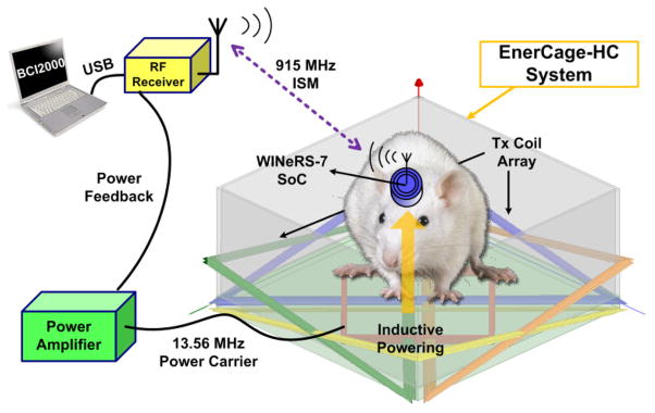
A conceptual view of the WINeR-7 system, which is fully compatible with our wirelessly-powered homecage system, called the EnerCage-HC [19], is shown in Fig. 1. The WINeR-7 system includes power management and wireless Tx, which allows it to be utilized in wireless and battery less experiments on animals freely behaving in a standard homecage. Section II describes different building blocks of the WINeR-7 system. The new wide swing DSCS-AFE architecture is presented in Section III, including DSCS FPGA demodulation algorithm. Section IV includes benchtop measurement results, followed by in vivo experiment results and conclusion in Sections V and VI, respectively.
Fig. 1.
A conceptual view of the inductively-powered wireless neural recording system-on-a-chip (WINeR-7) for long-term neural recording from small freely behaving animals (rats).
II. WINeR-7 System Architecture
A. Signal Path of the WINeR-7 Tx Unit
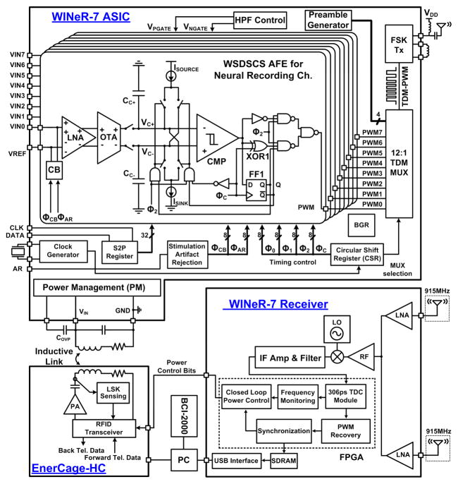
A simplified block diagram of the WINeR-7 ASIC is shown on the top side of Fig. 2, in which fully differential low-noise amplifiers (LNAs) amplify and filter neural signals with a gain of 100 V/V (40 dB) and an adjustable bandwidth (3–8 kHz). An operational transconductance amplifier (OTA) with variable-gm converts the LNA output to a current with 3-bit binary control over gm. The DSCS block pulse-width modulates the neural signal by comparing a pair of differentially charged and discharged capacitors, CC+ and CC−, via a rapid hysteresis comparator. The time division multiplexing block combines the eight PWM outputs of the DSCS array and generates the pseudo-digital TDM-PWM signal. A crystal-controlled circular shift register (CSR) is in charge of the AFE timing. A wireless Tx transmits the TDM-PWM signal through a wideband monopole antenna after frequency-shift keying (FSK). A serial-to-parallel (S2P) 32-bit register is also used to control various adjustable parameters among the eight channels.
Fig. 2.
Block diagram of the 8-channel DSCS-based wireless integrated neural recording (WINeR-7) system. Top: the transmitter unit with WINeR-7 ASIC and a few off-chip components, Bottom: the receiver unit and EnerCage-HC.
B. Power Path of the WINeR-7 Tx Unit
The power management (PM) unit includes an active dual supply rectifier, a battery charger, three regulators (LDOs), an automatic-resonance tuning (ART) block, and an amplitude-shift-keying (ASK) demodulator for data transmission. A power amplifier (PA) drives the Tx coil, L2, at the designated carrier frequency, fc = 13.56 MHz. The AC signal across the Rx LC-tank is rectified by the active rectifier. Three LDOs generate constant VDD = 2.1 V, VDDA = −0.3 V and VSS = −2.1 V. VDD and VSS are used together for the FSK Tx to provide a 4.2 V supply at a high Tx RF output power. On the other hand, VDDA and VSS are used together to provide a 1.8 V supply for the recording blocks, while lowering power consumption [20].
C. Receiver (Rx) Unit
The architecture of the WINeR-7 Rx unit, which block diagram is depicted at the lower right side of Fig. 2, is similar to the one we presented in [21] with 18 MHz of bandwidth. It demodulates and digitizes the incoming FSK-TDM-PWM signal (909/921 MHz, centered at 915 MHz), which is within the 902 to 928 MHz industrial-scientific-medical (ISM) band. For better coverage of the experimental arena, the WINeR-7 Rx has two antennas and LNAs, followed by a control circuit that connects the RF path with a stronger signal to a mixer, which down-converts the received RF signal to baseband (44/56 MHz) before demodulating the FSK signal in an FPGA [21]. The resulting baseband TDM-PWM signal is fed into a time-to-digital converter (TDC) in the same FPGA to generate digitized samples. These digitized samples are demultiplexed in the FPGA and buffered in a 1-Mbit SDRAM that is used to handle data transfer delays to a PC through a USB port. A general-purpose open-source platform, BCI2000 [22], runs on the PC to display the received neural signals on the screen and store them on a hard disk in real-time for further processing.
D. Closed-Loop Powering of WINeR-7 ASIC
When WINeR-7 is operated in the inductively powered mode, the most critical issue is the stabilization of the received power. This is challenging particularly when the distance and alignment between the power Tx and Rx coils constantly vary due to the movements of the freely behaving animal subject.
In WINeR-7 system, when the received power is out of the normal operation range, the frequency of the Tx VCO, which depends on its supply voltage, changes. In this case, the varying Tx frequency can be used to indicate the rectifier output voltage because the WINeR-7 Rx can detect the down-converted RF transmission frequencies by the TDC algorithm, introduced in Section III.C, and compare them with the fixed local oscillator frequency. This means that the Rx can detect the power supply voltage of the ASIC by monitoring the Tx frequency as the feedback signal, and correct it by controlling the PA output power. In practice, the PA power will be increased if the active rectifier output voltage on the Tx is less than its nominal value of 4.5 V. Conversely, when the rectifier output voltage > 4.5 V, the PA supply voltage is decreased. In this fashion, the closed-loop PA power control stabilizes the rectifier output.
III. Wide-Swing DSCS Analog Front End
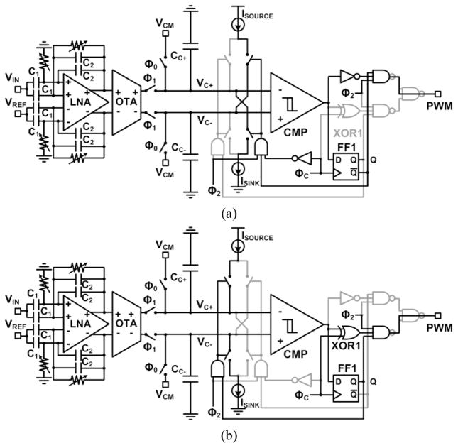
The previous DSCS-AFE [16] converted the amplified neural signal into a differential pair of currents, which were integrated in a pair of capacitors for a fixed time period. After the charging period, a pair of constant current source and sink discharged the stored charges to generate a PWM signal. Although the fabricated DSCS-AFE exhibited low-power, low noise, and robust operation, the dynamic range was limited only to half of the supply voltage. To eliminate the limitations of the DSCS-AFE architecture in [16], the wide swing DSCS-AFE architecture in Fig. 3 is proposed.
Fig. 3.
WINeR-7 wide swing DSCS-AFE operating schematic diagrams when, (a) VC+ > VC− and Q = 0, (b) VC+ < VC− and Q = 1.
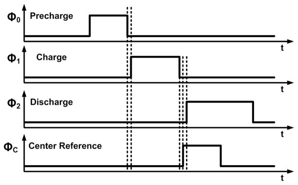
Four clock signals for the system are shown in Fig. 4, in which ΦC does not overlap with Φ1 and is faster ahead of Φ2. Therefore, the D flip-flop, FF1, in Fig. 2 can distinguish the two cases when it is triggered by ΦC prior to Φ2. During Φ2, if VC+ > VC−, the FF1 output, Q, is ‘0’; if VC+ < VC−, Q is ‘1’.
Fig. 4.
Four clock signals for the wide swing DSCS-AFE, used in WINeR-7.
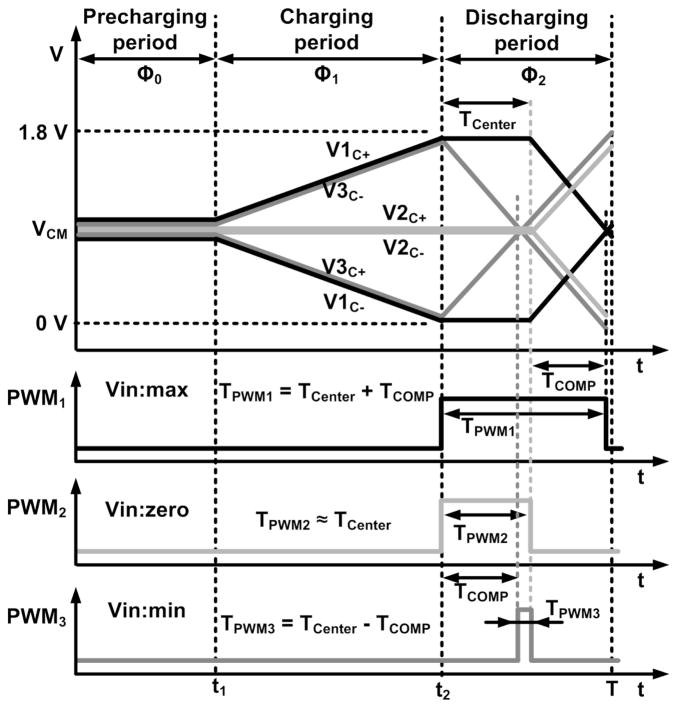
The operating waveforms of the system are shown in Fig. 5. In the new DSCS, half of the supply voltage VCM is used to precharge VC+ and VC− during a precharging period, Φ0. In addition, both VC+ and VC− can swing within the entire supply range. After a charging period, Φ1, the system verifies whether VC+ or VC− is higher prior to a discharging period, Φ2. Using this information, during Φ2, ISOURCE is connected to the lower output and ISINK is connected to the higher output. The PWM pulse width for VC+ > VC− should be longer than the PWM pulse width for VC+ < VC−. The center reference clock signal ΦC, which period, TCenter, is half of the Φ2 period, is used to distinguish the two cases. If VC+ > VC−, discharging of the output capacitors begins after ΦC changes from ‘1’ to ‘0’. V1C+, V1C−, and the resulting PWM1 in Fig. 5 demonstrate this case, in which TPWM = TCENTER + TCOMP. If VC+ < VC−, CC+ and CC− begin discharging immediately at Φ2 and TPWM = TCENTER − TCOMP. If VC+ ~ VC−, the resulting PWM pulse width, TPWM2, would be similar to TCENTER. When a minimum input is attained, V3C+, V3C−, and PWM3 are generated. The pulse width output can be formulated as follows:
| (1) |
| (2) |
Fig. 5.
Operating waveforms for different input voltages.
Two different operations of the system are shown in Fig. 3. First, the circuitry of Fig. 3a is activated when VC+ > VC− and Q = 0. Here, ISOURCE and ISINK are connected to VC− and VC+, respectively, after ΦC changes from ‘1’ to ‘0’ during Φ2. The PWM output is the inverted version of the CMP output. Therefore, TPWM = TCENTER + TCOMP. Second, the circuitry of Fig. 3b is activated when VC+ < VC− and Q = 1. Here, ISOURCE and ISINK are connected to VC+ and VC−, respectively, during Φ2. The PWM output is the exclusive ‘OR’ operation of the CMP output and ΦC. Therefore, TPWM = TCENTER − TCOMP.
A. LNA for Power Scheduling Operation
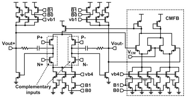
A schematic of the LNA and its common-mode feedback (CMFB) is shown in Fig. 6. The LNA uses a complementary input stage to increase the effective transconductance with a given current by two-fold [10]. Two-bit digital control over bias currents offers a programmable low-pass cutoff frequency, which is realized by gate-enabled bits B0 and B1 and change the tail currents of the main LNA and CMFB circuits. These control bits are also employed for power-scheduling mechanism, which was introduced in [6]. They keep the majority of the LNAs that are not being sampled in sleep mode, reducing their power consumption by disabling B0 and B1.
Fig. 6.
Schematic of the fully differential LNA with the CMFB circuitry.
B. Stimulus Artifact Rejection
The WINeR-7 system has a stimulus artifact rejection mechanism, shown in Fig. 2, for closed-loop neural interfacing, which requires simultaneous stimulation and recording. During stimulation, the LNA can be disconnected from the signal path by the stimulus-artifact rejection (AR) switches. In addition, the charge balancing (CB) switch in Fig. 2 connects the recording electrode to the reference electrode to ensure charge balancing between the two electrodes. This approach allows the accumulated charge at the sites to be minimized. These operations also help with rapid recovery of the neural recording function as soon as the stimulation is terminated.
C. DSCS FPGA Demodulation for the WINeR-7 System
Our conventional PWM-based WINeR-6 system required a PWM mask to separate PWM pulses of each channel because it did not have an accurate clock generator [6]. The DSCS in WINeR-7, on the other hand, does not require a PWM mask because it functions based on an accurate crystal-based clock signal. Without a PWM mask, the channel PWM pulse may disappear when the input is too low or PWM pulses from two channels may be combined when the input is too high. An FPGA TDC demodulation method was needed on the Rx side to correctly distinguish these special cases. Since the time bin of the WINeR-7 system is accurately defined by a crystal-based oscillator, once predefined marker signals followed by eight channel data are detected, the sequence of events within every time bin can be determined in the Rx, without requiring every channel to contain a mask.
For synchronization, the preamble generator block in Fig. 2 generates a sequence of four pulses equivalent to 1) zero, 2) maximum, 3) zero, and 4) half of the maximum amplitude, followed by a sequence of 8 PWM pulses from channels 1 to 8. The preamble bits are detected by the TDC method described in [21]. After detection of the preamble bits, eight time bins can be established following the end point of the preamble pulses, as shown in blue in Fig. 7. This will help the PWM signals to be accurately detected without any mask function on the Tx side by searching for the channel PWM signals within the time bins, where the minimum pulse width can be 0 s, and the maximum pulse width can be as same as the duration of the time bin.
Fig. 7.
WINeR-7 Rx TDC in the FPGA.
IV. WINeR-7 Measurement Results
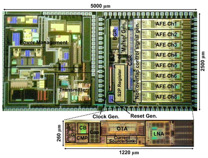
An 8-channel WINeR-7 prototype ASIC was fabricated in the TSMC 0.35-μm 4-metal 2-poly CMOS process. Fig. 8 shows the chip micrograph and floor planning, which occupies 5.0 × 2.5 mm2, including the padframe. In this implementation, each wide swing DSCS AFE channel occupies 1.22 × 0.26 mm2.
Fig. 8.
Die photomicrograph of the 8-channel wireless integrated neural recording (WINeR-7) SoC with the wide swing DSCS-AFE, implemented in the TSMC 0.35-μm CMOS (size: 5.0 × 2.5 mm2).
A. Wide Swing DSCS Performance
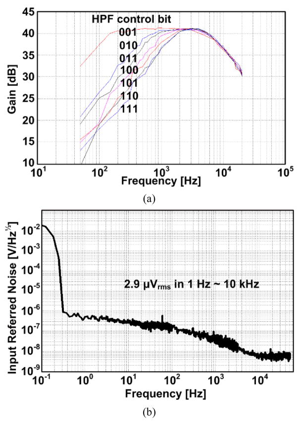
In the DSCS AFE channel, shown in Fig. 3, C1 was 8 pF, C2 was 80 fF, and Cc+ and Cc− were 10 pF each. The lower cutoff frequency of the LNA could be tuned from 1 to 800 Hz in 8 steps, and the higher cutoff frequency of the LNA was tunable from 3 to 8 kHz in 4 steps by voltage-controlled pseudo resistors. The fully differential design of the LNA yielded a power supply rejection ratio (PSRR) of 65.5 dB and a common mode rejection ratio (CMRR) of 56.4 dB, with an input referred noise of 2.9 μVrms in the frequency range of 1 Hz to 10 kHz for the LNA. The charging time Φ1 can be adjusted from 2.7 μs to 15.0 μs in 6 steps by programming the S2P register, leading to an adjustable gain of 200 V/V to 7800 V/V with the programmable transconductance from 7.43 μS to 50 μS in the OTA per channel.
The gain, bandwidth, and input referred noise of the LNA were measured from five chips, and the averaged characteristics are shown in Figs. 9a and 9b, respectively.
Fig. 9.
LNA measurements of (a) the gain and bandwidth and (b) the input referred noise.
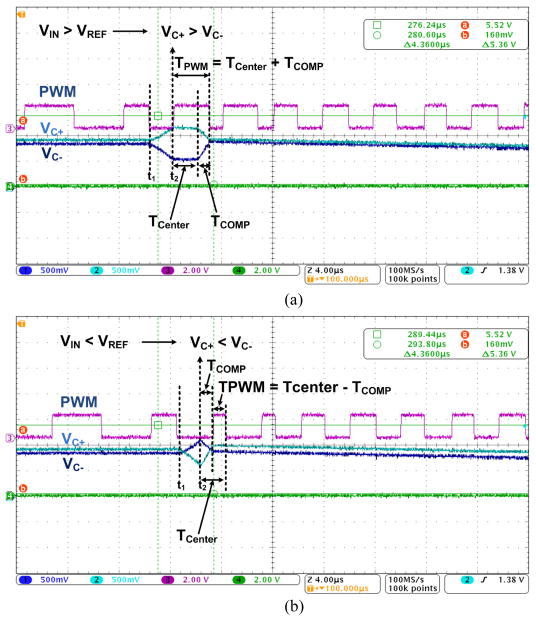
Fig. 10 presents some of the main operating waveforms in the DSCS-AFE for two different cases, similar to what was explained in Section III. The purple waveform is the TDM-PWM output signal, which combines the PWM signals from all eight channels. In Fig. 10a, the input is higher than VRef; thus, VC+ > VC−, and the measurement results of TPWM = TCENTER + TCOMP are attained. In Fig. 10b, the input is lower than VRef; thus, VC+ < VC−, and the measurement results of TPWM = TCENTER − TCOMP are attained. It should be noted that in both cases, the pulse width TPWM is proportional to the input signal.
Fig. 10.
WSDSCS-AFE measurement waveforms when (a) VC+ > VC− and Q = 0, (b) VC+ < VC− and Q = 1.
B. Stimulus Artifact Rejection
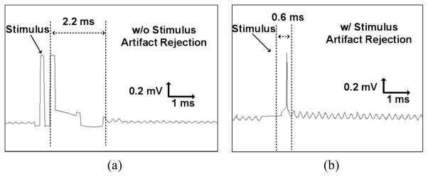
The stimulus artifact rejection function was tested in an in vitro setup with the custom-designed biphasic current-based stimulator described in [23]. A differential stimulation current of 840 μA was applied to a saline solution via electrodes. The stimulus artifact rejection and charge balancing mechanisms, which ensures that the residual charge is neutralized after biphasic stimulation, were triggered simultaneously in the WINeR-7 AFE units. To determine whether the AFE is saturated, a 1 kHz sinusoidal input signal was also applied in the saline, representing the desired extracellular neural signal. In this experiment, the AFE bandwidth was set to 0.4 to 8 kHz. First, the setup was tested without stimulus artifact rejection, the WINeR-7 Tx transmitted a recorded signal in the saline, and the Rx recovered and displayed it in BCI2000, as shown in Fig. 11a. In this figure, the LNA saturation is distinctly visible and it takes ~2.2 ms for the LNA to recover from saturation. When the same test was performed with stimulus artifact rejection active, the recovery time was decreased to less than 0.6 ms, as shown in Fig. 11b, and LNA saturation was avoided.
Fig. 11.
Recorded waveforms in the BCI2000 (a) without stimulus artifact rejection, (b) with stimulus artifact rejection.
C. Linearity Measurements with Battery Powered Setup
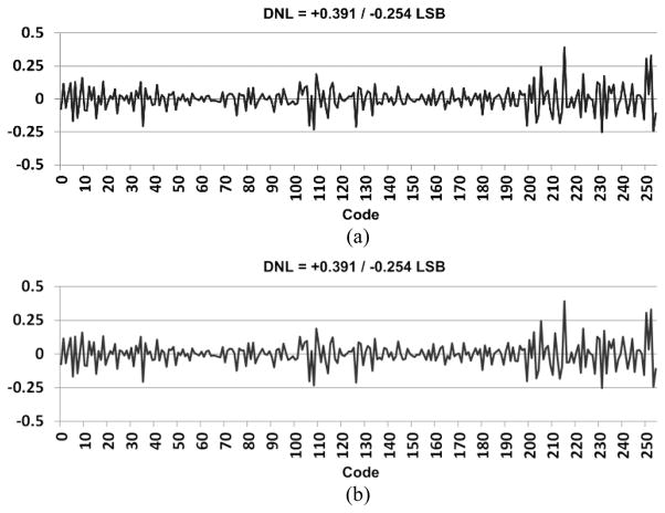
Bypassing the LNA block, the integral nonlinearity (INL) and differential nonlinearity (DNL) of the remainder of the WINeR-7 system were measured, as shown in [21]. By varying the DC input from rail to rail, i.e. 0 to +1.8 V, the increments in the 16-bit digitized value from the same channel were recorded on the Rx side, which was located 1.5 m away from the Tx antenna. Considering a dynamic OTA range, a window between +0.4 and 1.4 V was selected to measure the DNL and INL, and the LSB size was set to 3.9 mV for an expected 8-bit resolution. Fig. 12 presents the measured DNL and INL for the WINeR-7 prototype, which are within (+0.391, −0.254) LSB and (+0.353, −0.415) LSB, respectively.
Fig. 12.
(a) INL and (b) DNL measurements for the entire WINeR-7 system at a Tx-Rx distance of 150 cm with battery powered setup.
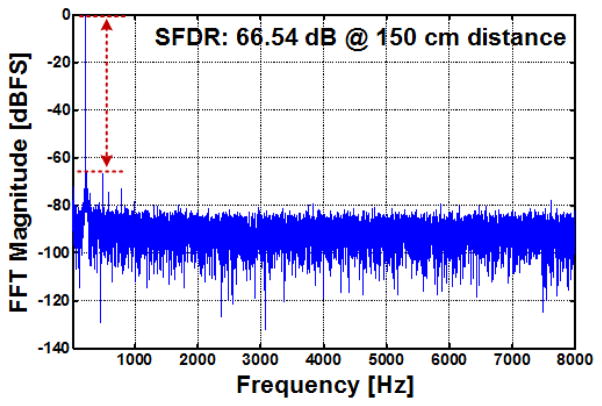
In addition to the INL and DNL, a tone test was conducted by applying a 217 Hz sinusoidal waveform with 3.2 VPP amplitude to ch-5 LNA output. The test results indicate a spurious-free dynamic range (SFDR) of 64.95 dB with a hardwired link. The SFDR and SNDR were 50.05 dB and 66.54 dB, respectively, during wireless operation with Tx-Rx separation of 150 cm, as shown in Fig. 13. Therefore, the effective number of bits (ENOB) is 8.02 bits at the nominal Tx-Rx distance of 1.5 m. The INL/DNL and the tone test were conducted with the battery powered setup. Because the inductive powering interferes with the RF link to a certain level, as described in the following session, and here the linearity of the system was measured without this interference.
Fig. 13.
Tone test measurements of the WINeR-7 system at a Tx-Rx distance of 150 cm with battery-powered setup.
D. WINeR-7 Noise Performance
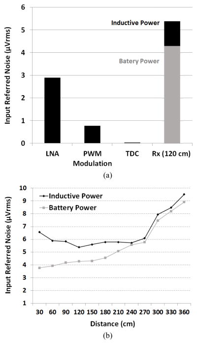
To analyze the noise contribution from different WINeR-7 blocks, noise measurements were performed in an unshielded laboratory environment in several configurations, similar to [21]. In each case, Fast Fourier Transform (FFT) was applied to 20 s of the recorded signal to derive its spectrum and refer it back to the input. In all noise measurements, the LNA bandwidth was set to 10 Hz ~ 8 kHz, whereas the input referred noise was integrated over the range of 1 Hz to 10 kHz.
The Tx-Rx distance was changed from 30 cm to 360 cm to observe the effect of Tx-Rx separation on the noise of the wireless link without shielding. The input-referred noise amplitudes for these measurements are shown in Figs. 14a and 14b. According to these graphs and our theoretical analysis in [24], the noise from the wireless Rx is the dominant source for the current 8-channel WINeR-7 system prototype, especially when the Tx-Rx separation is large. At the nominal Tx-Rx distance of 2 m, the linearity of the system is more than 8 bits considering the INL and DNL measurements in Fig. 12.
Fig. 14.
(a) Noise contributions of different WINeR-7 blocks at 21 kSps, (b) Noise measurement of the entire WINeR-7 vs. Tx-Rx distance.
An interesting observation in Fig. 14b illustrates that when the Tx-Rx separation is less than 120 cm in the inductively powered mode, a higher noise level is measured compared to battery-powered shorter distances, in which the input referred noise continues to drop. This is due to the RF interference from the wireless power transmitter in the EnerCage-HC. When the Rx antenna is close to the Tx, although Rx antenna can detect a strong RF signal at 915 MHz, the in-band harmonics of the power carrier signal at multiples of 13.56 MHz are also more prominent and the overall signal to noise-interference ratio drops. Considering the compromise between the SNR drop due to RF attenuation at longer distances and interference from power carrier harmonics at lower distances, Fig. 14b indicates that 120 cm is the experimentally-determined optimal Rx antenna position in this particular implementation of the wirelessly-powered neural recording system.
Table I compares the specifications of the WINeR-7 with other recently reported systems. WINeR-7 system shows good power/ch performance with wide LNA bandwidth for both local field potentials (LFP) and single unit activity (SUA). Only [11] has less power/ch compared with the proposed system at the same bandwidth. However, [11] requires an external FPGA for digital filtering for each channel, which make it difficult to implement in high channel-count recording systems. The input referred noise of the entire inductively-powered WINeR-7 system was measured by grounding the LNA inputs and conducting an FFT on the recorded signal for 10 s. Integration of these curves from 1 Hz to 10 kHz resulted in an input-referred noise of 5.38 μVrms at Tx-Rx distance of 120 cm.
Table I.
WINeR-7 Specifications and Benchmarking
| Publication | 2012 [12] | 2012 [11] | 2011 [25] | 2014 [13] | 2015 [27] | This work |
|---|---|---|---|---|---|---|
| Technology | 0.13-μm | 65-nm | 0.35-μm | 0.5-μm | 65-nm | 0.35-μm |
| Supply voltage (V) | 1.2 | 0.5 | 1.5 | 1.5, 3 | 0.5 | *1.8, **4.2 |
| Die size (mm2) | 5 × 5 | 0.13 | 3.3 × 3.3 | 2.85 × 3.84 | 2.4 × 2.4 | 5.0 × 2.5 |
| System size (cm3) | - | - | - | 2.2 × 1.1 × 0.5 | - | 3.5 × 2.5 × 0.8 |
| No. of channels | 96 | 1 | 4 | 9 | 64 | 8 |
| Total power (mW) | 6.5 | 0.005 | 0.42 | 5 | 13.225 | 51.4 |
| Power/ch. (μW) | 68 | 5.04 | 26.9 | 55.68 | 2.3 | 19.3 |
| Area/ch. (mm2) | 0.26 | 0.13 | - | - | 0.025 | 0.29 |
| Sampling rate (kSps/ch) | 31.25 | 20 | 63 (Max.) | 200 | 1 | 21.48 |
| LNA gain (dB) | - | > 32 | 51.9 – 65.5 | 39.35 | - | 40 |
| LNA input ref. noise (μVrms) | 2.2 | 4.9 | 3.12 | 4.58 | 1.25 | 2.90 |
| LNA HPF (Hz) | <1, 280 | 300 | 1.1 – 525 | 178 – 302 | 1 – 8 | 1 – 800 |
| LNA LPF (kHz) | 10 | 10 | 5.1 – 12 | 6.92 – 8.13 | 0.5 | 3 – 8 |
| System input ref. noise (μVrms) | - | - | - | 4.58 | - | ***5.38 |
AFE
Tx
Inductively-powered operation, BW: 1 Hz – 10 kHz, Distance: 120 cm
V. In Vivo Animal Experiments
To demonstrate the functionality of the WINeR-7 system, we conducted in vivo experiments in a wirelessly-powered standard homecage, with 30 × 28 × 18 cm3 dimensions [19]. Two 200 mF super-capacitors were connected to the positive and negative rectifier outputs to supply the mobile unit when the inductive coupling was weak due to the large distance or misalignment of the power Tx-Rx coils. Additional details of the closed-loop external powering system can be found in [19], [28], [29].
A custom designed 16-channel multi-electrode array (Tucker Davis Technologies; Alachua, FL) was stereotactically implanted in a male Sprague-Dawley rat (>350 g; Charles River Laboratories; Wilmington, MA) for chronic simultaneous recording the LFP from the CA1 and CA3 areas of the hippocampus. All work was conducted in accordance with the National Institutes of Health Guide for the Care and Use of Laboratory Animals and approved by Emory University’s Institutional Animal Care and Use Committee.
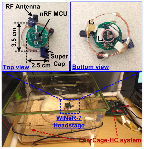
The in vivo test setup of WINeR-7 mobile unit in the inductively-powered homecage, also known as the EnerCage-HC system, is shown in Fig. 15 with the top and bottom views of the mobile unit and power Rx coils, L3 and L4. Eight of the electrodes were connected to the WINeR-7 to record LFPs, while the animal carried the WINeR-7 headstage inside the EnerCage-HC system. The geometries of L3 and L4 were optimized based on the design procedure in [30] to maximize the PTE, leading to diameter/number of turns of 3.5 cm/2 and 1 cm/6, respectively (see Table I in [19] for more details). The WINeR-7 mobile unit is positioned not to be reachable to the animal during in vivo experiment. Neural recordings were performed while the animal was awake and freely moving. Fig. 16 shows 8-channel LFP recordings by the inductively-powered WINeR-7 system from a freely behaving rat in the EnerCage-HC system with a wide bandwidth of 1 Hz to 10 kHz. The SNR in these waveforms is lass than desired, but they clearly show the LFP patterns.
Fig. 15.
In vivo test setup of WINeR-7 headstage for inductively-powered homecage system.
Fig. 16.
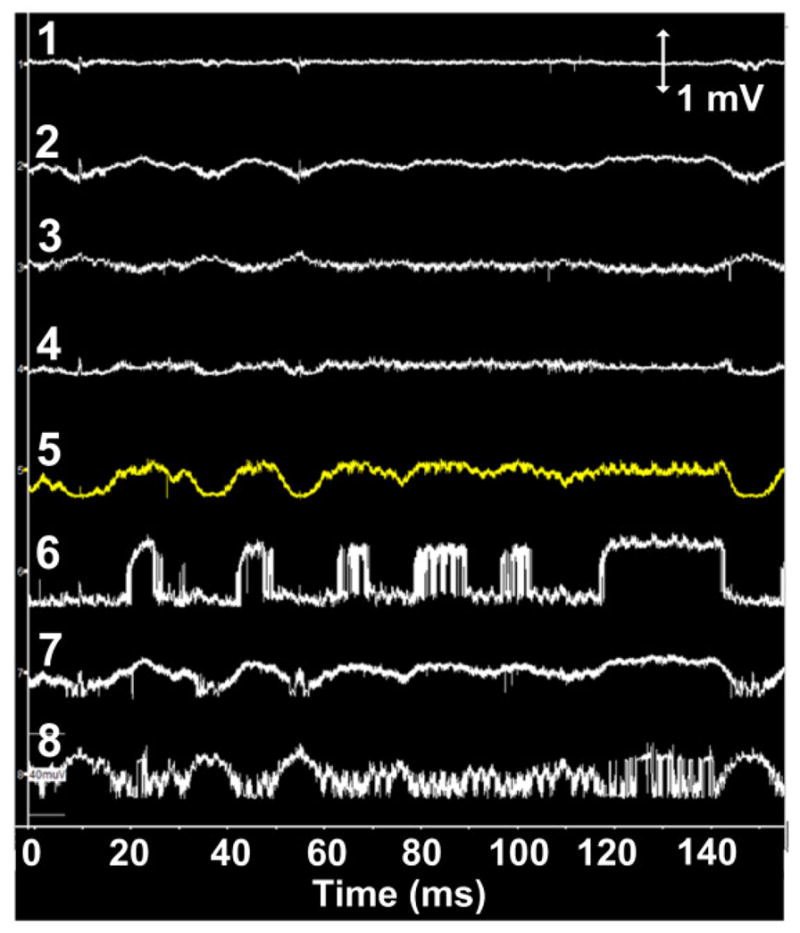
8-channel LFP recordings from the WINeR-7 system for a freely-moving rat in EnerCage-HC system with a bandwidth of 1 Hz to 10 kHz.
VI. Conclusions
An 8-channel WINeR-7 system with a novel wide swing DSCS AFE architecture has been developed and tested in vivo without batteries in a wirelessly-powered environment. The new DSCS AFE converts neural signals into currents to charge capacitors, which voltages are then compared based on a time and amplitude based logic to convert the neural signal amplitudes to pulse width (PWM). The presented DSCS-AFE achieves amplification, filtering, sampling, and amplitude-to-time conversion (ATC), simultaneously, while consuming a small amount of power. In this system, the closed-loop inductive power control with optimal coil design provides high PTE while maintaining the received power at the headstage constant despite animal movements. The WINeR-7 system enables neuroscientists to eliminate cables from their electro-physiology experiments without adding the burden of carrying large battery payloads on the freely behaving animal subjects, or shortening the duration of the trial. The ultimate goal is to enable acquiring high-density and high-fidelity neural signals over unlimited periods of time with smaller and lighter Rx coil inside the wirelessly-powered homecage.
Acknowledgments
This work was supported in part by the National Institutes of Health grants 5R21EB009437, 1R21EB018561, and the National Science Foundation under awards ECCS-1408318 and IIP-1346416.
The authors would like to thank members of the GT-Bionics lab for their help in the original design and benchtop testing of the WINeR-7 system.
Biographies

Seung Bae Lee (S’08-M’15) received the B.S. degree in electrical engineering from Hanyang University, Seoul, Korea, in 2007. He received his M.S. and Ph.D. degrees in Electrical and Computer Engineering from the Georgia Institute of Technology in 2010 and 2014, respectively. He is currently a mixed-signal design engineer at Texas Instruments Inc., Dallas, TX, USA. He is involved in system-on-chip designs for various sensor modules.

Byunghun Lee (S’11) received the B.S. degree from Korea University, Seoul, South Korea, and the M.S. degree from Korea Advanced Institute of Technology (KAIST), Daejeon, South Korea, in 2008 and 2010, respectively. From 2010 to 2011, he worked on wireless power transfer systems at KAIST as a design engineer. He is currently pursuing his Ph.D. degree in Electrical and Computer Engineering at Georgia Institute of Technology. His research interests include analog/mixed-signal IC design and wireless power transfer systems for biomedical applications.
Mehdi Kiani (S’09) received the B.S. degree from Shiraz University, Shiraz, Iran, and the M.S. degree from Sharif University of Technology, Tehran, Iran, in 2005 and 2008, respectively. He received his M.S. and Ph.D. degrees in Electrical and Computer Engineering from the Georgia Institute of Technology in 2012 and 2013, respectively. He is currently an Assistant Professor in the Department of Electrical Engineering at the Pennsylvania State University. His research interest is integrated circuits and systems design for bio application. He was the recipient of the Georgia Tech Sigma Xi Best PhD Thesis Award, and Georgia Tech Chih Foundation Research Award for excellent research in the fields of engineering and health sciences.
Babak Mahmoudi received a BSc in electrical engineering from University of Tehran in 1999, a MSc in bio-electrical engineering from Iran University of Science and Technology in 2003 and a Msc and PhD in Biomedical engineering from the University of Florida in 2009 and 2011 respectively. In 2004, he was invited to RIKEN Brain Science Institute, Japan, as a visiting scholar. Dr Mahmoudi was the recipient of a Howard Hughes Medical Institute fellowship at the University of Florida in 2009. He completed postdoctoral trainings in the University of Miami and the Emory University School of Medicine where he was awarded a NIH NRSA fellowship for translational research in neurology. His research interests are focused on designing intelligent neural interface systems with application in neurorehabilitation and neuromodulation therapies. He has published more than 40 peer reviewed papers in the area of neural interface systems.

Robert Gross MD, PhD is the MBNA/Bowman Professor of Neurosurgery at Emory University, with appointments in Neurology, Neuroscience and Biomedical Engineering. He completed his neurosurgical residency at Albert Einstein College of Medicine, followed by fellowship training in functional and stereotactic neurosurgery at University of Toronto and epilepsy surgery at Yale University. He is presently Director of the Emory MD/PhD Program, and co-founder and Director of the Emory Neuromodulation and Technology Innovation Center (ENTICe). In addition, he directs the Translational Neuroengineering Research Group, which focuses on neuromodulation for epilepsy and movement disorders, including closed-loop feedback strategies. Dr. Gross is active in organized neurosurgery, holding a variety of positions in neurosurgical and neurological societies including Secretary/Treasurer of the Amercian Society for Stereotactic and Functional Neurosurgery, and is an editor for several major journals. Dr. Gross’s research interests include neuromodulation and novel surgical techniques for movement disorders, depression, epilepsy and memory. His research has been continuously supported by the NIH and various foundations.
Maysam Ghovanloo (S’00–M’04–SM’10) received the B.S. degree in electrical engineering from the University of Tehran, Tehran, Iran, in 1994, the M.S. degree in biomedical engineering from the Amirkabir University of Technology, Tehran, Iran, in 1997, and the M.S. and Ph.D. degrees in electrical engineering from the University of Michigan, Ann Arbor, in 2003 and 2004, respectively. From 2004 to 2007, he was an Assistant Professor at the Department of Electrical and Computer Engineering, NC-State University, Raleigh, NC. He joined the faculty of Georgia Institute of Technology, Atlanta, GA in 2007 where he is currently an Associate Professor and the Founding Director of the GT-Bionics Lab in the School of Electrical and Computer Engineering. He has authored or coauthored more than 150 peer-reviewed publications.
Contributor Information
Seung Bae Lee, GT-Bionics lab, School of Electrical and Computer Engineering at the Georgia Institute of Technology, Atlanta, GA 30308, USA.
Byunghun Lee, GT-Bionics lab, School of Electrical and Computer Engineering at the Georgia Institute of Technology, Atlanta, GA 30308, USA.
Mehdi Kiani, GT-Bionics lab, School of Electrical and Computer Engineering at the Georgia Institute of Technology, Atlanta, GA 30308, USA.
Babak Mahmoudi, Department of Neurosurgery at Emory University.
Robert Gross, Department of Neurosurgery at Emory University.
Maysam Ghovanloo, GT-Bionics lab, School of Electrical and Computer Engineering at the Georgia Institute of Technology, Atlanta, GA 30308, USA.
References
- 1.Donoghue JP. Bridging the brain to the world: a perspective on neural interface systems. Neuron. 2008;60:511–521. doi: 10.1016/j.neuron.2008.10.037. [DOI] [PubMed] [Google Scholar]
- 2.Harrison RR, Kier RJ, Chestek CA, Gilja V, Nuyujukian P, Ryu S, Greger B, Solzbacher F, Shenoy KV. Wireless neural recording with single low-power integrated circuit. IEEE Trans Neural Syst Rehab Eng. 2009 Aug;17(4):322–329. doi: 10.1109/TNSRE.2009.2023298. [DOI] [PMC free article] [PubMed] [Google Scholar]
- 3.Schwartz AB, Cui XT, Weber DJ, Moran DW. Brain-controlled interfaces: movement restoration with neural prosthetics. Neuron. 2006 Oct;52:205–220. doi: 10.1016/j.neuron.2006.09.019. [DOI] [PubMed] [Google Scholar]
- 4.Miranda H, Gilja V, Chestek CA, Shenoy KV, Meng TH. HermesD: a high-rate long-range wireless transmission system for simultaneous multichannel neural recording applications. IEEE Trans Biomed Circuits and Systems. 2010 Jun;4(3):181–191. doi: 10.1109/TBCAS.2010.2044573. [DOI] [PubMed] [Google Scholar]
- 5.Kringelbach ML, Jenkinson N, Owen SLF, Aziz TZ. Translational principles of deep brain stimulation. Nature Reviews Neuroscience. 2007 Jun;8(8):623–635. doi: 10.1038/nrn2196. [DOI] [PubMed] [Google Scholar]
- 6.Lee SB, Lee H, Kiani M, Jow U, Ghovanloo M. An inductively powered scalable 32-channel wireless neural recording system-on-a-chip for neuroscience applications. IEEE Trans Biomed Circ and Sys. 2010 Dec;4(6):360–371. doi: 10.1109/TBCAS.2010.2078814. [DOI] [PMC free article] [PubMed] [Google Scholar]
- 7.Fan D, Rich D, Holtzman T, Ruther P, Dalley JW, Lopez A, Rossi MA, Barter JW, Salas-Meza D, Herwik S, Holzhammer T, Morizio J, Yin HH. A wireless multi-channel recording system for freely behaving mice and rats. PLoS ONE Neuroscience. 2011 Jul;6(7):e22033. doi: 10.1371/journal.pone.0022033. [DOI] [PMC free article] [PubMed] [Google Scholar]
- 8.Harrison RR, Charles C. A low-power low-noise CMOS amplifier for neural recording applications. IEEE J Solid-State Circuits. 2003 Jun;38(6):958–965. [Google Scholar]
- 9.Wattanapanitch W, Fee M, Sarpeshkar R. An energy-efficient micropower neural recording amplifier. IEEE Trans Biomed Circ and Sys. 2007 Jun;1(2):136–147. doi: 10.1109/TBCAS.2007.907868. [DOI] [PubMed] [Google Scholar]
- 10.Zhang F, Holleman J, Otis BP. Design of ultra-low power biopotential amplifiers for biosignal acquisition applications. doi: 10.1109/TBCAS.2011.2177089. accepted for publication in IEEE Trans. Biomed. Circ. and Sys. [DOI] [PubMed] [Google Scholar]
- 11.Muller R, Gambini S, Rabaey J. A 0.013mm2, 5μW, DC-coupled neural signal acquisition IC with 0.5 V supply. IEEE J Solid-State Circuits. 2012 Jan;47(1):232–243. [Google Scholar]
- 12.Gao H, Walker RM, Nuyujukian P, Makinwa KA, Shenoy KV, Murmann B, Meng TH. Hermes-E: A 96-channel full data rate direct neural interface in 0.13 μm CMOS. IEEE J Solid-State Circuits. 2012 Apr;47(4):1043–1055. [Google Scholar]
- 13.Borna A, Najafi K. A low power light weight wireless multichannel microsystem for reliable neural recording. IEEE J Solid-State Circuits. 2014 Feb;48(2):439–451. [Google Scholar]
- 14.Muller R, Le H, Li W, Ledochowitsch P, Gambini S, Bjorninen T, Koralek A, Carmena JM, Maharbiz MM, Alon E, Rabaey JM. A miniaturized 64-channel 225μW wireless electrocorticographic neural sensor. Digest of technical papers IEEE Intl Solid State Cir Conf. 2014 Feb;:412–413. [Google Scholar]
- 15.Cong P, Chaimanonart N, Ko WH, Young DJ. Wireless and batteryless 10-bit implantable blood pressure sensing microsystem with adaptive RF powering for real-time laboratory mice monitoring. IEEE J Solid-State Circuits. 2009 Dec;44(12):3631–3644. [Google Scholar]
- 16.Lee SB, Lee B, Gosselin B, Ghovanloo M. A dual slope charge sampling analog front-end for a wireless neural recording system. Proc IEEE 36th Engineering in Medicine and Biology conference. 2014 Aug;:763–766. doi: 10.1109/EMBC.2014.6944287. [DOI] [PMC free article] [PubMed] [Google Scholar]
- 17.Rieger R. Variable-Gain, Low-Noise Amplification for Sampling Front Ends. IEEE Trans Biomed Circ and Sys. 2011 Jun;5(3):253–261. doi: 10.1109/TBCAS.2010.2104320. [DOI] [PubMed] [Google Scholar]
- 18.Xu G, Yuan J. Performance analysis of general charge sampling. IEEE Trans Circuits Syst II, Exp Briefs. 2005 Feb;52(2):107–111. [Google Scholar]
- 19.Lee B, Kiani M, Ghovanloo M. A smart wirelessly-powered homecage for long-term high-throughput behavioral experiments. IEEE Sensors. 2015 doi: 10.1109/JSEN.2015.2430859. [DOI] [PMC free article] [PubMed] [Google Scholar]
- 20.Lee B, Kiani M, Ghovanloo M. A triple-loop inductive power transmission system for biomedical applications. IEEE Trans Biomed Circuits Syst. 2015 doi: 10.1109/TBCAS.2014.2376965. [DOI] [PubMed] [Google Scholar]
- 21.Lee SB, Yin M, Manns J, Ghovanloo M. A wideband dual-antenna receiver for wireless recording from animals behaving in large arenas. IEEE Transactions on Biomedical Engineering. 2013 Jul;60(7):1993–2004. doi: 10.1109/TBME.2013.2247603. [DOI] [PMC free article] [PubMed] [Google Scholar]
- 22.Yin M, Ghovanloo M. A low-noise clockless simultaneous 32-channel wireless neural recording system with adjustable resolution. Analog Integrated Ckts & Sig Proc. 2011 Mar;66(3):417–431. BCI-2000 homepage, [Online]. Available: http://www.bci2000.org. [Google Scholar]
- 23.Lee H. Ph D dissertation. Georgia Institute of Technology; Atlanta, GA: 2014. A Power-Efficient Wireless Neural Stimulating System with Inductive Power Transmission. [Google Scholar]
- 24.Yin M, Ghovanloo M. Using pulse width modulation for wireless transmission of neural signals in multichannel neural recording systems. IEEE Trans on Neural Sys Rehab Eng. 2009 Aug;17(4):354–363. doi: 10.1109/TNSRE.2009.2023302. [DOI] [PMC free article] [PubMed] [Google Scholar]
- 25.Azin M, Guggenmos DJ, Barbay S, Nudo RJ, Mohseni P. Abattery-powered activity-dependent intracortical microstimulation IC for brain–machine–brain interface. IEEE J Solid-State Circuits. 2011 Apr;46(4):731–745. [Google Scholar]
- 26.Rolston JD, Laxpati NG, Gutekunst C, Potter SM, Gross RE. Spontaneous and evoked high-frequency oscillations in the tenanus toxin model of epilepsy. Epilepsia. 2010 Nov;51:2289–2296. doi: 10.1111/j.1528-1167.2010.02753.x. [DOI] [PMC free article] [PubMed] [Google Scholar]
- 27.Muller R, Le H, Li W, Ledochowitsch P, Gambini S, Bjorninen T, Koralek A, Carmena JM, Maharbiz MM, Alon E, Rabaey JM. A minimally invasive 64-Channel wireless uECoG implant. IEEE J Solid-State Circuits. 2015 Jan;50(1):344–359. [Google Scholar]
- 28.Jow U, McMenamin P, Kiani M, Ghovanloo M. EnerCage: A Smart Experimental Arena with Scalable Architecture for Behavioral Experiments. IEEE Transactions on Biomedical Engineering. 2014 Jan;61(1):139–148. doi: 10.1109/TBME.2013.2278180. [DOI] [PMC free article] [PubMed] [Google Scholar]
- 29.Jow U, Kiani M, Huo X, Ghovanloo M. Towards a smart experimental arena for long-term electrophysiology experiments. IEEE Trans Biomed Circ and Sys. 2012 Oct;6(5):414–423. doi: 10.1109/TBCAS.2012.2211872. [DOI] [PMC free article] [PubMed] [Google Scholar]
- 30.Kiani M, Jow U, Ghovanloo M. Design and optimization of a 3-coil inductive link for efficient wireless power transmission. IEEE Trans Biomed Circuits Syst. 2011 Dec;5(6):579–591. doi: 10.1109/TBCAS.2011.2158431. [DOI] [PMC free article] [PubMed] [Google Scholar]


