

Abstract
With the expanding interest in cellular responses to dynamic environments, microfluidic devices have become important experimental platforms for biological research. Microfluidic “microchemostat” devices enable precise environmental control while capturing high quality, single-cell gene expression data. For studies of population heterogeneity and gene expression noise, these abilities are crucial. Here, we describe the necessary steps for experimental microfluidics using devices created in our lab as examples. First, we discuss the rational design of microchemostats and the tools available to predict their performance. We carefully analyze the critical parts of an example device, focusing on the most important part of any microchemostat: the cell trap. Next, we present a method for generating on-chip dynamic environments using an integrated fluidic junction coupled to linear actuators. Our system relies on the simple modulation of hydrostatic pressure to alter the mixing ratio between two source reservoirs and we detail the software and hardware behind it. To expand the throughput of microchemostat experiments, we describe how to build larger, parallel versions of simpler devices. To analyze the large amounts of data, we discuss methods for automated cell tracking, focusing on the special problems presented by Saccharomyces cerevisiae cells. The manufacturing of microchemostats is described in complete detail: from the photolithographic processing of the wafer to the final bonding of the PDMS chip to glass coverslip. Finally, the procedures for conducting Escherichia coli and S. cerevisiae microchemostat experiments are addressed.
1. Part I: Introduction
Microfluidic technology has enjoyed considerable success and interest in recent years. Microfluidic devices have been used for everything from miniaturization of molecular biology reactions to platforms for cell growth and analysis (Bennett et al., 2008; Cookson et al., 2005; Danino et al., 2010; Hersen et al., 2008; Hong et al., 2004; Kurth et al., 2008; Lee et al., 2008; Rowat et al., 2009; Taylor et al., 2009; Thorsen et al., 2002). A driving factor for increased use of microfluidics is the potential for more productive experiments, that is, accomplishing the same or more using fewer resources (primarily less reagents, consumables, and time). Furthermore, microfluidic devices offer the unrivaled ability to precisely control and perturb the environment of single cells while capturing their behavior using high resolution microscopy. In this report, we will concentrate on how to design, build, operate, and analyze data from single cells growing in the chambers of high-throughput microfluidic devices. We will focus primarily on a device built to monitor the growth of Saccharomyces cerevisiae (yeast) in a dynamically changing environment as a case study. This device is known in our lab as the MDAW or Multiple Dial-A-Wave device.
In our lab we strongly believe in the importance of acquiring single cell trajectories from our experimental runs. This requires the ability to track single cells over the course of an experiment, which generally lasts 24–72 h. Indeed, of all technologies available in molecular biology, microfluidics alone offers the ability to track the behavior of a large number of individual cells over the course of an experiment. While other technologies, such as flow cytometry, allow the acquisition of single cell data, the experimenter cannot track each individual cell in time. This leads to “snap shots” of how the population as a whole changes in time, but does not capture how individual cells progress over the course of an experiment.
The difference between the techniques can be illuminated easily if one thinks of a population of cells containing a desynchronized genetic oscillator. In this case much depends on the waveform of the oscillator. For oscillators with sinusoidal output, the population will appear bimodal with a large portion of the cells spread between the two modes. However, for an oscillator with output similar to a triangle wave, the cells will be uniformly distributed between all phases of oscillation and therefore the population will have a fairly evenly distributed set of fluorescent values. Of course the behavior of a real oscillator can be somewhere between these extremes, but the point is that looking at the progression of a population as a whole does not tell you everything about its dynamics. For example, in each of the cases mentioned above, other explanations are possible, such as the transient of a bistable switch, or even a genetically mixed population of cells. In contrast, using a microfluidic device to follow the temporal dynamics of single cells in such a population would allow one to easily see if any cells were oscillating.
While microfluidics is powerful, flow cytometry has the ability to capture a large amount of data quickly, much more quickly than it can be done in traditional microfluidics. For this reason, microfluidic and flow cytometry should be thought of as complimentary, instead of competing, technologies. We often find it useful to first characterize our genetic circuits using flow cytometry, testing as many media or inducer concentrations as possible, to look for behavior indicative of interesting dynamics. Once these conditions are determined we follow up with the more powerful but involved microfluidic experiments.
Thus in the context of this report we will be talking about microfluidic chips designed to capture single cell data over the 1–3 days of the experiment. Unfortunately this limits the architecture of such a chip due to the difficulty of tracking cells. Regrettably cells such as yeast or especially Escherichia coli have few unique features which can be used to distinguish them from their brethren. The full details of this will be discussed in a later section describing cell tracking, but suffice it to say, the only truly unique characteristic all cells possess visible by phase contrast microscopy is their position in time. As an added complexity, cells such as yeast or E. coli are so fast growing they can quickly fill both a trap and the camera’s field of view. Once the trap is full, the colony of cells will begin to move in flows resembling particulate flows (Mather et al., 2010). These flows are due to pressure exerted by the colony on the walls of the trap. Due to this movement, phase contrast images of a colony’s growth must be taken often, usually every 30 s to a minute, to prevent excessive movement between images.
Unfortunately, this requirement of frequent imaging imposes a physical limit to the size of the chip, usually determined by the speed of the microscope hardware. Even state of the art, fully automated microscope hardware such as the Nikon TI system, cannot autofocus, acquire phase contrast plus 3–4 fluorescent images, and then move to a new stage location in less than 4–5 s and sometimes as many as 7–10 s depending on the acquisition parameters. This limits the number of chambers and hence the number of independent experiments to at most 8–14, if the 1-min interval between phase images is followed. Of course one also has to worry about overexposing cells to fluorescent excitation light, which can easily kill even the hardiest of cells rather quickly. Thus while phase contrast images are acquired every minute, we normally only capture fluorescent images every 5 min. Since 4 out of 5 acquisitions will not contain fluorescence capture (usually the longest step) this decreases the overall acquisition time somewhat. However, even if the phase contrast interval is lengthened the scope hardware will end up being the limiting factor in determining how large a chip can become. Of course microfluidic chips have been created with thousands of chambers (Taylor et al., 2009); however, these devices cannot capture the type of single cell trajectory data that smaller devices can, at least with current microscope technology.
The types of microfluidic experiments we will discuss here pretty much require the latest in microscope hardware for reasons mentioned above. Automation of most microscope tasks is critical, such as stage movement, phase ring and fluorescent cube changing, and shutter control. Moreover taking images every minute for days on end requires an automated focus routine, which luckily most microscope manufactures can readily provide. This also requires large amounts of hard disk space and equally important a rigorous method for space management, with backup procedures in place to prevent catastrophic data loss. Moreover the sensitivity of the camera used is extremely important. While the background fluorescence (a bound for the minimum detectable signal) of yeast and E. coli cells is easily observed using CCD cameras even a decade old, one should always use the most sensitive camera available to minimize the exposure time and hence phototoxicity caused by the fluorescent excitation lamp. The overall idea is that while older hardware may allow you to capture some data like that we discuss here, newer hardware will allow you to capture more data with a higher quality and with less damage to your cells.
1.1. The design of a microfluidic chip
To design a microchemostat chip useful for the type of experiments described in the introduction, one has to know a small amount about fluid mechanics at the microscale. We will briefly describe the physics behind microfluidics here, but the reader is directed to more complete texts if desired (Beebe et al., 2002; Brody et al., 1996; Nguyen and Wereley, 2002; Whitesides et al., 2001a). Those that have not studied fluid mechanics in depth do not have to worry because making a functional microchemostat is not too difficult. The first thing to understand is how fluid flows at the microscale of a microfluidic device. From fluid mechanics we know that there are essentially two major flow regimes: laminar and turbulent flow. Laminar flows contain highly predictable, parallel flow streams resulting in fairly easy to model profiles. In contrast, turbulent flows are unpredictable, difficult to model computationally, and contain complicated flow patterns such as eddies and vortices (there is also a transition regime between these two flow types). For microchemostat devices, the flow will be exclusively laminar as explained below. However, to determine the flow type in a arbitrary system, the most important parameters are the type of fluid used, the dimensions of the fluid channels and the fluid’s velocity in these channels. The relationship between these parameters can be expressed as the Reynolds number (Re), which is a dimensionless quantity useful for determining the dominant profile in a flow system. The Reynolds number is defined by
| (14.1) |
where ρ is the density of the fluid, υ is the mean fluid velocity, Dh is the hydraulic diameter of the channel (a value which depends on the channels dimensions; see Nguyen and Wereley, 2002), and μ is the fluid’s viscosity (Beebe et al., 2002). The Reynold’s number represents a ratio between the inertial forces and the viscous forces of a fluid’s flow. Empirically it has been determined that flows with a high Reynold’s number (Re > 103), indicating the dominance of inertial forces, will be turbulent while low Reynolds number flows (Re < 1) will be exclusively laminar (Brody et al., 1996). Typical parameter values for microchemostats with an aqueous fluid are given in Table 14.1. Due to the low Reynolds number in these chips flow is laminar.
Table 14.1.
Typical physical parameter values for microchemostat devices used in synthetic biology
| Parameter | Variable | Value | Units |
|---|---|---|---|
| Density of water | ρ | 1 × 10³ | kg m−3 |
| Viscosity of water (dynamic) | μ | 1 × 10⁻³ | kg m−1 s−1 |
| Hydraulic diameter | Dh | 1 × 10⁻⁴–1 × 10⁻⁶ | m |
| Mean fluid velocity | υ | 1 × 10⁻⁴–1 × 10⁻⁶ | m s−1 |
| Reynolds number | Re | 1 × 10⁻²–1 × 10⁻⁶ | N/A |
1.1.1. Mixing in microchemostat devices
A major consequence of laminar flow is that mixing will only occur due to diffusion, since bulk mixing relies on some type of turbulent flow. An important way to view the effect of diffusion in a microchemostat is to consider the diffusion length scale, which describes the one dimensional distance a molecule can be expected to travel in a given amount of time. The relationship is given as (Beebe et al., 2002)
| (14.2) |
where d is the distance a molecule travels, D is the molecule’s diffusion coefficient, and t is the elapsed time. Since the distance traveled by a molecule is proportional to the square root of the elapsed time, diffusion will become more important at smaller length scales. For a specific example consider the Atto 655 dye, expected to diffuse 10 μm in 0.1 s, but taking over 1000 s to diffuse 1 mm. Diffusion coefficients for representative molecules often encountered in microchemostats are given in Table 14.2.
Table 14.2.
Diffusion coefficients for ions and molecules commonly used in microfluidic chemostats
| Name | Molecular weight (Da) | Diffusion coefficient (cm2 s−1) | Reference |
|---|---|---|---|
| Sodium ion (Na+) | 22.98 | 1.3 × 10⁻⁵ | Lide (2004) |
| Glucose | 180.16 | 6.7 × 10⁻⁶ | Lide (2004) |
| Atto 655 dye | 528 | 4.3 × 10⁻⁶ | Dertinger et al. (2007) |
| Bovine albumin | 67,000 | 5.9 × 10⁻⁷ | Young et al. (1980) |
As expected the diffusion coefficient tends to increase with increasing molecular weight and this is important to compensate for when using a tracer dye to monitor nutrient transport. For example, as can be seen in Table 14.2, one should be careful using Atto 655 dye as a surrogate for bovine albumin transport, or any high molecular weight protein, due to their order of magnitude difference in diffusion coefficients. Another important concept regarding diffusive transport in microchemostats is the Péclet number, which is another dimensionless quantity given by
| (14.3) |
where L is the is the characteristic length scale, which in a microchemostat corresponds to the channel width. The Péclet number represents a ratio between advection and diffusion of a substance. Conceptually it can be thought of as the ratio of how far “downstream” a molecule is carried versus how far it diffuses across the channel in a given unit of time. In microfluidic systems reliant on diffusive mixing, knowledge of the Péclet number is critical for designing functional microchemostats. To determine the length required (Δym) for effective diffusive mixing of a substance, the following relationship is useful (Stroock et al., 2002):
| (14.4) |
| (14.5) |
Thus, Eq. (14.4) indicates that for two channels with equivalent Péclet numbers, the narrower one will require a shorter length for complete mixing. This statement is important because often in the design of microchemostats one wishes to carefully manage the volumetric flow rate to ensure optimal reagent use. As derived in the next section, there is often a combination of parameter values for the dimensions of a channel which result in the same resistance (and hence the same volumetric flow rate for a given pressure gradient). Often many of these parameter values will result in the same Péclet numbers as well. For example, two channels, one with a twofold greater width and a twofold smaller length will have the same resistance and equivalent Péclet numbers. However, the length required for diffusive mixing will differ as described by Eq. (14.4) and this is important to consider in the design.
1.1.2. Calculating flow rates and pressure drops
While there has been some debate as to whether the general Navier-Stokes equation is applicable to the small scale of microfluidic devices, recent work has demonstrated that this is so and suggested that previously observed deviations were due to experimental error (Bao and Harrison, 2006). As a consequence of laminar flow in a microchemostat chip, the Navier-Stokes equations reduce to a simple analog of Ohm’s law. This equation is
| (14.6) |
where ΔP is the pressure drop across a channel, Q is the volumetric flow rate, and R is the resistance of the channel. This allows the simple calculation of flow rate in a chip as a function of external pressure and channel resistance. To calculate R the dimensions of the channel have to be considered. For cylindrical channels, the resistance is given by the Hagen–Poiseuille equation, equal to
| (14.7) |
where μ is the fluids viscosity, L is the length of the channel, and r is the radius of the channel. For the rectangular channels usually encountered in microchemostats, this equation has to be modified somewhat, taking into consideration the ratio between the width of the channel and the height, known as the aspect ratio. For channels with a low aspect ratio (w ≈ h), the equation for channel resistance is given by (Beebe et al., 2002)
| (14.8) |
while Eq. (14.8) appears complicated, in practice it is not too difficult to work with if desired. Note the 1/n5 term in the infinite sum. Since this term quickly approaches zero for increasing n, only the first five terms need to be considered to get a reasonable approximation. However, this equation can be further reduced when using a chip with high aspect ratio channels (w ⋙ h). Usually this is the case, as typical channel heights in a yeast or E. coli chip will be in the range of 5–10 μm while the width will range from 60 to 300 μm. In this situation, the bracket term in Eq. (14.8) will tend to zero and the resistance simply becomes
| (14.9) |
Using Eqs. (14.6) and (14.9) the flow rates in a microfluidic chip can be solved for in a straightforward manner, using methods similar to nodal analysis for electrical circuits. First consider a sample microfluidic chip depicted in Fig. 14.1A and B, which is shown diagrammatically in stick form to make analysis easier. For each internal node labeled a–d in the figure, the flow entering must equal the flow exiting due to the conservation of mass. This is analogous to Kirchhoff’s first law for electrical circuits. Thus for all nodes in the device
| (14.10) |
where n is the number of channels joining at the node. Furthermore, note that the system will be solved once the internal pressures at the nodes are determined, since the flow rates between nodes can be found from Eq. (14.6). We will use the system described in Fig. 14.1 as an example to demonstrate how to solve such a problem. The first step would be to come up with a diagram similar to Fig. 14.1A, with the external ports and internal nodes clearly labeled.
Figure 14.1.
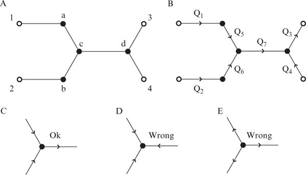
Overview of how to conceptually set up microfluidic flow problems. (A) Stick diagram of a conceptual microfluidic device. External ports with specified pressures (open circles) are labeled 1–4. Internal junctions (whose pressures will be solved for, closed circles) are labeled a–d. (B) Same diagram as in part A, except the port and junction numbers are removed for clarity. Volumetric flows to be solved for are given by Q1–7. (C–E) Overview of the correct way to set up flow directions in a microfluidic junction, while obeying the conservation of mass. Part C has the correct setup, containing both inlets and an outlet. Part D is incorrect since there are only inlets. Part E is also incorrect since there are only outlets.
Next label the current flow directions with arrows between nodes as shown in Fig. 14.1B, while making sure to obey the conservation of mass. Note that you may not know the direction of flow beforehand (in fact that may be why you are doing this exercise), however, this does not matter initially. As long as the conservation of mass is followed the system can be solved properly. If your initial flow direction guess is incorrect, its solution will be negative, indicating the opposite is the true direction of flow. After this step is complete, develop a system of equations describing the flow in each node. For the example system
| (14.11a) |
| (14.11b) |
Next use Eq. (14.6) to substitute the pressure and resistance for the current
| (14.12) |
| (14.13) |
Since Eqs. (14.12) and (14.13) contain cumbersome fractions, it is useful to define the conductance G as the inverse of the resistance R,
| (14.14) |
By substituting the conductance for the resistance in Eqs. (14.12) and (14.13) we get the following:
| (14.15) |
| (14.16) |
| (14.17) |
| (14.18) |
Expanding and rearranging we get
| (14.19) |
| (14.20) |
| (14.21) |
| (14.22) |
Or in matrix form
| (14.23) |
Equation (14.23) is a linear system which can be either solved manually or with the aid of a computer program such as Excel or Matlab. Of course the above procedure can become tedious, especially for larger microchemostat chips and a method which lends itself to automation would be preferred. To develop such a system first rearrange Eqs. (14.11a) and (14.11b) to put all currents on the LHS
| (14.24a) |
| (14.24b) |
Now arrange Eqs. (14.24a) and (14.24b) into matrix form
| (14.25) |
which can be expressed as
| (14.26) |
where C is an i × j matrix called the connectivity matrix for a chip with i nodes and j channels. The C matrix is unique for each chip and should be specified from a graph of the chips architecture. The is a vector of length j representing the flows in the chip. Since is unknown we need to use Eqs. (14.6) and (14.14) to substitute flows for pressures and conductivities
| (14.27) |
Thus the flow vector can be split into two vectors as shown in the RHS of Eq. (14.27). The first vector contains only known values, being the external pressures and conductances of the channels connected to these ports. The second vector contains known conductances and the unknown internal node pressures which we are interested in solving for. Separating the conductances from the pressures we get
| (14.28) |
or
| (14.29) |
where G is a j × k matrix of j channels and k external ports containing conductance values, is a k length vector specifying the known external port pressures, H is a j × l matrix of j channels and l internal nodes containing conductance values and is a l length vector containing the unknown internal port pressures. Combining Eqs. (14.26) and (14.29) we get
| (14.30) |
| (14.31) |
| (14.32) |
where and I = CH. Note that Eq. (14.32) is the same as Eq. (14.23) and can be solved in the same ways. To solve the flow profiles for an arbitrary chip, the C, G, and H matrices need to be specified, which can be done once the connectivity and channel geometries are decided upon. To automate this process our lab uses a custom matlab script, written by a former graduate student, called moca. This program has been extended to calculate how the pressure in each external port changes in time as fluid flows from the inlet ports to the outlets.
Alternatives to nodal analysis are commercial software package employing finite element techniques to solve for the flows in a more exact manner. An example of such a software package is the program Comsol, which contains an internal software package explicitly set up to solve microfluidics problems. For the design of microchemostats, this level of computation can be helpful for certain parts of the chip. For example, Comsol, unlike nodal analysis techniques, can model the diffusive transport of nutrients in complicated geometries such as cell traps or junctions. Moreover transient behavior of the chip, including how a cell chamber will respond to pressure surges, can be easily modeled in Comsol but not using nodal analysis techniques. As an additional advantage, Comsol has the ability to create models directly from Autocad files, which can save a considerable amount of time. However, software programs such as Comsol are quite expensive and nodal analysis techniques are generally fine for designing basic microchemostats.
1.1.3. Designing a microchemostat chip
To design a microchemostat device one has to know a little about the overall fabrication process. The complete details will described in the fabrication section, but we will give a brief description here. The general process is known as soft-photolithography, originally developed for the semiconductor industry. When used for microchemostats, soft-photolithography creates reusable master molds with chemicals known as photoresists. Photoresists are viscous chemicals spun on silicon wafers to very precise heights. When exposed to ultraviolet (UV) light, the photoresist cross-links and becomes resistant to developer solvent, while the uncross-linked photoresist remains susceptible. To make a microchemostat, a negative image of the device’s features is placed between the photoresist and the UV light source. An example of such a mask is shown in Fig. 14.2. When exposed, the UV light will pass through the clear sections containing the device’s features, while the dark regions will prevent the background from being cross-linked. After the uncross-linked photoresist is removed with developer, the process is repeated for the next layer. To align multiple layers, an aptly named mask aligner machine is used. This machine contains a microscopy setup so alignment patterns between the previous photoresist layer and the current mask can be viewed. Once all layers have been completed, the wafer can be used to produce an almost unlimited amount of microchemostat devices.
Figure 14.2.
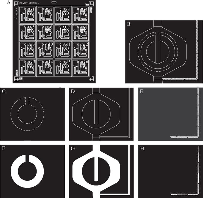
Overview of the mask design process for microchemostat devices. (A) Overview of an Autocad file with the features of the microchemostat shown in white. Note the alignment features in the lower left and upper right corners. Each chip is individually numbered so those defective can be tracked. (B) Close-up of the cell trap region from the Autocad file shown in part A. This region contains features of three different heights, which are in different layers of the Autocad file. The cell trap will be of height 3.5 μm and is shown with dashed lines. The central chamber will be 10 μm and is shown with solid lines. The staggered herringbone mixers (SHM) will be of height 3 μm above the 10 μm mixer channel height for a total of 13 μm. Note the overlap between layers. When layers meet there should always be an overlap to compensate for small errors in mask alignment. (C-E) Each layer from part B is shown individually, with the cell trap in part C, the cell chamber in part D, and the SHM features in part E. When sent for printing, the layers should be displayed individually as is shown here. (F–H) Depiction of what the mask will look like after printing. The features of the device will be clear (white in the figure) to allow UV light to pass, while the background is black.
When designing a device, the first step is to layout the architecture in a vector graphics software program such as Autocad. While it is possible to use other programs, such as Adobe Illustrator, in general Autocad is superior since it is designed for precision fabrication. Furthermore companies offering extremely high resolution mask printing generally require Autocad files. Student versions of Autocad are reasonably priced and offer more capability than is necessary for designing microchemostats. During the design stage, one needs to decide how many different channel heights will be in the device. For example, the cell trap might be 3.5 μm while the channel network is 10 μm, as is often the case for yeast chips. All features with the same height should be on the same layer in the Autocad file to make work easier (see Fig. 14.2).
When designing a chip with multiple layers, care must be taken to provide an accurate method for alignment during fabrication. During the alignment process one will need to look through the mask at the pattern from a previous layer and adjust the controls so the current mask will perfectly overlap. As shown in Fig. 14.3 there are three degrees of freedom which need to be manipulated during the alignment process: xy translation and rotation. To make sure the wafer and mask are in perfect alignment, two locations must be viewed on the wafer to compensate for small errors in rotation. The center of the mask essentially determines the axis of rotation. The further away the two locations are from the center (and each other), the easier small errors in rotation will be to see.
Figure 14.3.
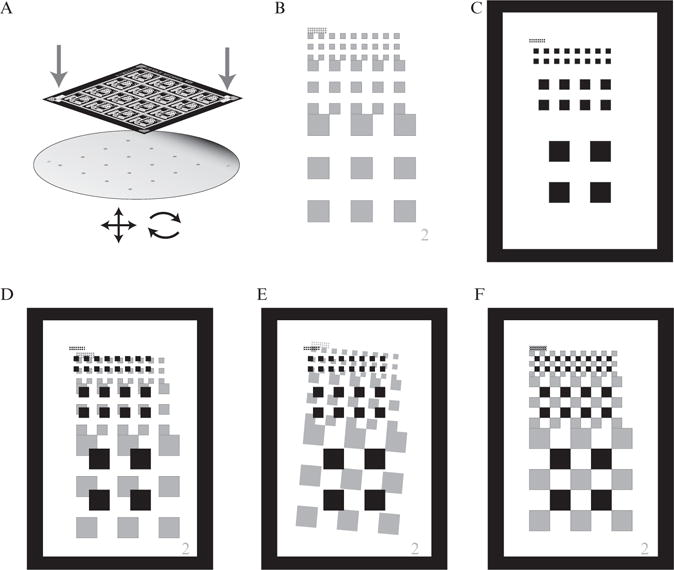
Overview of the alignment pattern for microchemostat devices. (A) Overview of the alignment process, with a mask shown above a wafer containing a previously deposited photoresist layer with alignment patterns. The mask aligner will have controls to compensate for both translation and rotation (bottom arrows). The arrows pointing down on the mask show the alignment pattern location. (B) Alignment pattern present on the wafer from the previous photoresist deposition. Each layer will require a separate alignment pattern; the layer number is shown in the lower right. The pattern is composed of sets of squares whose sides are reduced by half in each iteration. (C) Alignment pattern present on the mask. The clear window surrounding the squares allows the fabricator to view the pattern from the previous layer. The objective is to make the points of the squares from the mask and the previous layer touch. (D) Mask and wafer out of alignment by xy translation only. (E) Mask and wafer out of alignment by rotation only. (F) Mask and wafer in perfect alignment.
In Fig. 14.2A the alignment locations are in the lower left corner and upper right corner of the mask, the furthest possible from the center. The alignment features shown in Fig. 14.3 are designed to have coarse and fine features to speed the alignment process and work quite well in practice. To align the patterns, one adjusts the mask aligner controls until the points of the squares meet in all locations. Note that a separate alignment pattern will be necessary for each layer other than the first, since the mask’s viewing window will cross-link the photoresist (and therefore remove the wafer’s alignment pattern for the layer) after each alignment and exposure.
When considering a device design and alignment pattern, it is critical that the thinner layers are fabricated before the thicker ones. For example, a 3.5-μm layer should always be fabricated before a 10-μm layer. We have found that if thicker layers are fabricated first, the later layers will spin unevenly, since the larger features from the previous layer prevent an even coating of the wafer. Furthermore, it is important not to increase the height too greatly between consecutive layers, since this limits the contrast in the mask alignment process. Recall that mask alignment occurs after spinning the current (uncross-linked) photoresist layer, which covers all previous (cross-linked) photoresist layers. Fortunately, the wafer’s alignment pattern on the previously cross-linked photoresist layer can usually be seen through the current layer. However, if the height ratio between the two layers is greater than about 5:1, the contrast becomes so poor that it is difficult to see the wafer’s alignment pattern. In general, we try and limit the height ratio to 3:1, since mask alignment is generally the most difficult and frustrating part of fabrication.
Once the alignment strategy is settled upon, the device features can be laid out in Autocad. For this purpose simple rectangles are usually sufficient, but arc segments can be used if more complex shapes are desired. We have found that curved sections are superior for cell containing channels, since they prevent clogging. For areas of the chip not expected to contain cells, rectangular segments meeting at sharp corners are fine. When designing channels, all features should be closed objects in Autocad, there should be no open segments. While resulting in lines across channels, these will not be printed since lines are considered to be of infinitesimal thickness by the printer and only closed regions are recognized (compare Fig. 14.2D and G). Ensuring that all regions are closed in Autocad will not only make printing easier, but also facilitates importing into Comsol and Illustrator.
In general when laying out features, one must consider the tradeoff between compacting the device into as small a space as possible and maintaining usability. For example, placing two ports closer than 2 mm is not advisable since it makes it extremely difficult to plug in the port lines upon setup. Furthermore having a channel pass closer than a 1-mm to a port should also be avoided since it can be damaged if the port hole is punched incorrectly. Along these same lines, there should be at least 1 mm between a feature and the edge of the chip, so when the PDMS slab is diced into individual units no features are damaged.
In addition, when two layers are contiguous there should be some overlap between them to compensate for the small errors in alignment that inevitably occur. For example, in Fig. 14.2B the cell trap layer overlaps the cell chamber layer. If the layers were designed with no overlap a small alignment error could create a gap between them resulting in a nonfunctional chip. Even with the alignment patterns described in Fig. 14.3 and a meticulous alignment procedure, small errors will occur and can be compensated for with layer overlap. When layers overlap the total height is usually a smooth transition between the height of the thicker layer alone and the sum of the heights of the overlapping layers. As shown in Fig. 14.2B the cell chamber wall starts out at 10 μm and gradually increases to ~14 μm in the overlapping area. This phenomenon should be remembered when modeling the flow profile of a device in Comsol for example, since a ~40% change in height due to overlap will have a large effect on the channel’s resistance.
Another common mistake results from layers unintentionally intersecting due to small alignment errors. This can create fluidic “short circuits” and nonfunctional chips. The solution here is to again make sure an adequate margin is present between nonintersecting layers to compensate for fabrication problems. Most importantly, keep in mind the concept of tolerances. While the feeling for this comes from experience, always assume that some fabrication error is inevitable rather than trying to come up with the most beautiful design in Autocad. The best design will be one that can tolerate some fabrication error and still work properly, even if it is not the most “compact” design. The size of the channels is also affected by these same concepts. We have found that channel widths smaller than 60 μm should be avoided since they are prone to clogging with debris that can enter the chip (often residual PDMS). Moreover long channels should generally be 10 μm or more in height, also to prevent clogging.
Of course the ultimate limitation for microfluidic design is the resolution of the printer making your masks. This limit usually comes into play before that imposed by the UV light source or the photoresist. We use a company named CAD/Art for mask printing which has a 20,000-dpi printer. While this is normally adequate for microchemostats, higher resolution options used in the semiconductor industry are available at far greater expense. Using this process, we have been able to make features separated by as little as 13 μm as long as they are on the same layer. However, even this is dependent on the type of photoresist used. For example the spatial resolution of a thinner photoresist, like that used to make a 10-μm layer, is generally greater than that of a thicker resist, used for making a 35-μm layer. General guidelines for recommended channel dimensions are given in Table 14.3. Note it is certainly fine to make channels having dimensions other than those given in the table and for specialized features (like high resistance cell feeding channels) this may be necessary. For the normal fluidic “backbone” of the chip, the channel dimensions listed in Table 14.3 should be fine.
Table 14.3.
General guidelines for channel dimensions in microchemostat chips
| Channel type | Organism | Width range | Height range |
|---|---|---|---|
| General flow network (no cells) | Any | 60–100 μm | 10–15 μm |
| High flow channel (no cells) | Any | 300–400 μm | 20–45 μm |
| General cell channels | E. coli | 150–300 μm | 6–15 μm |
| yeast | 200–300 μm | 10–15 μm | |
| mammalian | 200–300 μm | 25–35 μm | |
| Cell trap | E. coli | Varies | 1 μm |
| Yeast | Varies | 3.55 μm | |
| Mammalian | Varies | 25 μm |
While the general guidelines listed so far should be useful for creating a microchemostat device, as a case study we will describe our design process for an updated dial-a-wave chip. The device, called MFD005a, was designed as an improved version of the chip described in Bennett et al. (2008). The chip is designed to grow cells reliably in a monolayer and cope with high growth by flushing excess cells into a waste port. The chip is also designed to generate arbitrary, time varying inducer concentrations, so the cell’s response to a dynamic environment can be recorded. Often we use the chip to generate arbitrary waveforms, such as sine waves, square waves, or waves having a random period component. The waves generated by the device have high temporal accuracy and the chip is easy to use. An overview of the device is shown in Fig. 14.4. The chip has five external ports, which is a reduction from eight in the Bennett chip. Reducing ports saves on consumables and eases setup, so finding the minimum number necessary to produce a working chip should always be a design goal. The chip is designed to use hydrostatic pressure and therefore no pumps are required of any kind for operation. We have found that hydrostatic pressure gives the most reliable, steady, and cost effective means of controlling the pressures in a microchemostat device. In a later section, we will describe our use of linear actuators to alter the inlet hydrostatic pressure of our device and why this is advantageous compared to other means such as syringe pumps.
Figure 14.4.
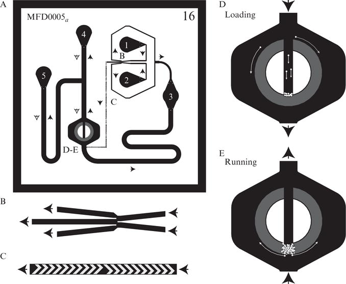
Overview of the MFD005a chip and components. (A) Overview of the MFD005a chip’s architecture. Flow directions in each segment during running conditions are given by black arrows, during loading conditions by white arrows. Note that only flow from ports 4, 5, and across the cell chamber changes direction during loading. Letters represent locations of the features described in other parts of the figure. External ports are numbered 1–5. Each port is described in Table 14.4. (B) Depiction of the DAW junction. Flow direction is indicated by the black arrows. The two inlets on the right come from ports 1 and 2. The flow from the inlets converges in a ratio dependent on the inlet pressures of each. The middle fork of the junction leads to the cell chamber while the two outer forks lead to port 3, the cell and shunt waste port. (C) Depiction of the staggered herringbone mixers (SHM) which reduce the channel length required for mixing. These mixers immediately follow the DAW junction and continue until just before the cell chamber. (D) Overview of trap region of the MFD005a chip under loading conditions. This trap is known as the yeast doughnut trap. Black region represents the cell chamber with a height of 10 μm. Gray region is the actual cell trap, with a height of 3.525 μm. White circles represent cells entering from the cell port and either passing around the trap to the cell and shunt waste (port 3), or entering the central channel and moving to the trap entry barrier. The yeast cells are slightly too large to move into the trap directly without “flicking” the cell line to assist in their entry. (E) Cell trap upon running of an experiment. Cells begin to grow in the trap and the colony expands (black arrows). Eventually the colony fills up the gray region near where they were loaded. The growth of the cells will force some out of the trap into the outer channel where they will be efficiently carried away to the waste port (white arrows). Over the course of the experiment the cell colony will expand to fill the entire trap.
The role of each port of the MFD005a chip is given in Table 14.4. When an experiment is running, fluid will enter from ports 1 and 2 which meet at the dial-a-wave junction (Fig. 14.4B). The DAW junction has two inlets and three outlets. As described in a later section, the ratio of the inputs from port 1 and 2 leaving the junction to the cell chamber is determined by each port’s pressure. Excess fluid is diverted through a shunt network to port 3, which is a waste port. Fluid leaving the central fork of the junction for the cell chamber travels through a long channel where it is mixed into a uniform concentration by staggered herringbone mixers (SHM). The ingenious SHM mixers (as shown in Fig. 14.4C) are designed to induce a corkscrew effect in the fluid stream and increases the surface area available for mixing (Stroock et al., 2002; Williams et al., 2008). Since mixing only occurs due to diffusion in a microchemostat, as mentioned in Section 1.1.1, this increase in surface area will logarithmically reduce the length of a channel necessary for uniform mixing.
Table 14.4.
Role and pressures for each port in the MFD005a device
| Port | Description | Contents | Run inH2O | Load inH2O |
|---|---|---|---|---|
| 1 | Inlet 1 for DAW | Media + inducer + tracking dye | 25 | 25 |
| 2 | Inlet 2 for DAW | Media | 25 | 25 |
| 3 | Cell and shunt waste | dH2O | 5.5 | 5.5 |
| 4 | Alternate outlet | dH2O | 6 | 17 |
| 5 | Cell port | Media + cells | 6 | 18 |
All pressures are given in inH2O above the height of the microscope stage.
Even with the help of SHM features, mixing still requires a length which depends on the log of the Péclet number (Stroock et al., 2002). Thus a central question when designing our device was how long to make the mixing channel from the DAW junction to the cell port. If the channel were too short, the two inputs would not be completely mixed, resulting in a nonuniform and uneven concentration profile over the cell culture. However, making the channel too long is also disadvantageous since it increases the delay time for a signal to propagate the length of the channel. To find the optimum channel length, we require knowledge of the flow velocities as a function of the external port pressures. This is a good example of the usefulness of the modeling techniques mentioned in Section 1.1.2. Using nodal analysis or Comsol it is easy to determine the flow rates and hence the Péclet number for various substances and flow regimes. We performed just such an analysis when designing the MFD005a device to determine the necessary channel length for efficient mixing, shown in Fig. 14.5.
Figure 14.5.
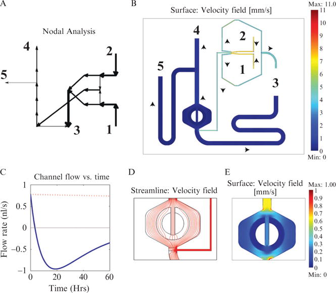
Comparison of a nodal analysis tool written in Matlab (moca) and Comsol (finite element analysis package). (A) Graph from the moca matlab script depicting flows for the device pictured in Fig. 14.4A. The arrow thickness and direction represent the volumetric flow in a channel section of the device. Numbers are the external ports of the device. (B) Flow velocity through the same chip modeled using Comsol. The magnitude of the velocity is given by the channel’s color, while the direction is indicated by the black arrows. Numbers are again the external ports. The MFD005a geometry was loaded directly from Autocad, simplifying setup. (C) Flow profile of a channel section over the course of an experiment. In previous designs, we have had problems with backflow problems over the course of an experiment, as the fluid level in the external ports is altered by flow. Modeling an experiment’s flow profile using nodal analysis helped to solve these problems, resulting in a redesign of the diversion channel’s dimensions and using larger syringes. The blue line represents fluid flow using 1-ml syringes and the red dashed line 60-ml syringes. (D) Streamline plot showing the path fluid particles take upon moving through the cell trap. While this plot was generated under running conditions, the streamlines are very similar for loading conditions (the direction of flow of course is opposite). Note that only about one fourth of the flow enters the central channel, most flow is directed around the trap. Hence, when loading, most cells will not enter the trapping region. (E) Plot of the velocity field inside the trap region. Note that the velocity is lowest inside the trap itself and considerably higher in the outer channel region. This allows nutrients to be continually replenished from the outer channel into the cell trap and helps remove cells once they outgrow the trap.
After mixing, fluid from ports 1 and 2 enters the cell chamber and proceeds to the outlet ports 4 and 5. Fluid also enters a diversion channel and exits at port 3. By controlling the height of port 3 relative to ports 4 and 5, one can set the ratio of fluid passing through the chamber versus exiting through the diversion channel. Modulation of this diversion ratio is important for controlling the flow velocity across the cell chamber. For example, say you wanted to minimize the flow velocity in the cell chamber why still retaining functionality of the DAW junction. Without a diversion channel you could lower the height of the input ports 1 and 2 relative to 4 and 5 and reduce the flow velocity in the cell chamber. However, this would also reduce the flow velocity in the mixing channel between the DAW junction and the cell chamber. This reduction in mixing channel velocity would increase the delay time for fluid transit and negatively impact the chips function. With a diversion channel, an alternative is to maintain the height difference between ports 1–2 and 4–5 and instead lower port 3. This would increase the ratio of fluid entering the diversion channel and hence lower the fluid velocity in the cell chamber. This is another example of flow modeling’s usefulness, since the diversion channel’s length is critical for determining the amount of fluid diverted for a given height change.
Modeling also allowed us to solve a problem with flow reversal (backflow) in the diversion channel, which would sometimes occur over the course of an experiment in a previous version of this device. The plot in Fig. 14.5C represents a time dependent solution for the flow profile in the device’s diversion channel, compensating for pressure changes due to fluid movement over the course of an experiment. The solid blue line represents the flow rate when small diameter syringes are used for the outlets. The fluid level in these syringes increases in height rapidly for a given volumetric flow. Under certain conditions this height increase can be large enough to change the flow velocity in the chip. When the blue line crosses the zero point of the y-axis, flow reversal has occurred. The red dashed line represents the same initial setup using larger diameter 60 ml syringes. These syringes undergo far less increase in height for a given volumetric flow than the smaller syringes and therefore it takes far longer (much longer than an experiment would last) to reach a flow reversal condition. The solution was reached by redesigning the diversion channel to have a greater resistance and by using larger syringes. While this model was created using nodal analysis, it could also be done in Comsol.
1.1.4. Design of an improved DAW junction
Another opportunity for flow modeling came from designing the DAW junction. As mentioned previously, this junction is designed to combine the inputs from ports 1 and 2 of the MFD005a device in a precise ratio depending on the input pressures. By controlling the input pressures as a function of time, one can generate precise waves of inducer concentration and hence expose cells to a fluctuating environment. To set the mixing ratio, the pressure of one input is increased and the other decreased by the same amount. By changing the input pressures in an opposing manner, the flow rate out of the junction remains constant and hence the downstream flow rates are not altered (this can be easily demonstrated using nodal analysis). Of course, by the conservation of mass, if the total outlet flow does not change, then the total inlet flow must not change either. Instead the ratio between the two inlet flows changes.
Initially one might think that a simple T-junction would suffice to reliably mix the two inputs streams. Indeed, when the output is derived nearly equally from both inputs (near a 50% mixing ratio), a T-junction works fine. However, as depicted in Fig. 14.6, a T-junction does not work well for skewed output ratios, when most of the output is coming from only one of the inputs. As an example of a skewed ratio, consider when 95% of the output is coming from input 1 and the other 5% is coming from input 2, with a total flow rate of 1 nl/s. Under these conditions the input 1 flow rate will be 0.95 nl/s, while the input 2 flow rate will be only 0.05 nl/s. Going further, for a mixing ratio of 100%, the input 1 flow rate will be 1 nl/s and the input 2 flow rate will be 0 nl/s. Of course in practice, even with the most accurate system, an entirely stagnant flow is impossible to achieve. In reality this situation represents an unstable equilibrium, prone to backflow. If attempting this with a real device, either a true 100% ratio will not be achieved, or (more likely) fluid from input 1 will begin to flow into input 2. This backflow situation will result in improper mixing of the input 2 source, preventing the system from functioning properly if later switched. For example, consider if backflow had occurred for 1 h and then the system was switched, from a mixing ratio of 100% to 0%. In this situation, the residual flow from input 1 would have to flow back again before fresh input 2 media could again enter the junction. Depending on the residual flow rate from input 1 to 2, this could take a considerable amount of time.
Figure 14.6.
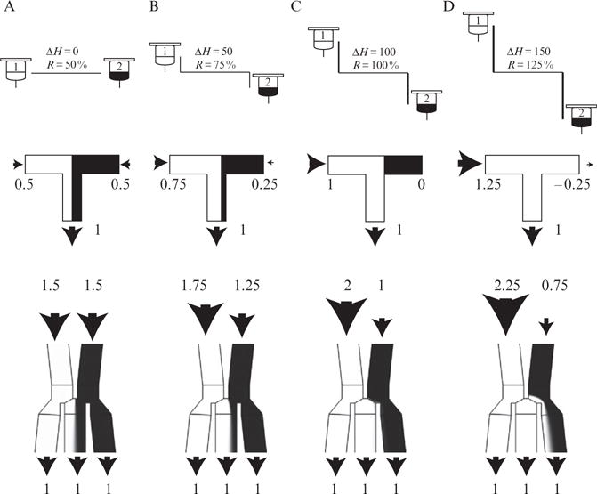
Comparison of a T-junction to our improved DAW junction for combining different source fluids in precise ratios. The figure depicts four mixing ratios from 50% to 125% and compares the performance of each junction. Note that since the system is symmetrical, flows for mixing ratios from −25% to 50% will be the reverse of those shown here. Mixing ratios above 100% or below 0% indicate complete diversion of one of the inputs to the shunt. deltaH (please write it as greek lowercase delta and english uppercase H) is an arbitrary unit of distance. (A). Mixing ratio of 50% (R = 50%), corresponding to equal flows from both reservoirs. A fluorescent dye has been added to reservoir 1, displayed in white as it would be seen under the microscope. Top portion of the figure depicts the reservoirs at equal height (ΔH = 0). Middle portion of the figure depicts a T-junction, each input flow is 0.5 nl/s, for a total flow of 1 nl/s. Bottom portion represents the DAW junction. Each inlet has a flow of 1.5 nl/s, for a total inlet flow of 3 nl/s. Note the smooth interface between fluid streams, as diffusion has not yet been able to cause appreciable mixing. (B) Mixing ratio of 75%. The height of the port 1 reservoir has increased while the corresponding port 2 reservoir has decreased by an equivalent amount. Both junctions continue to perform well. Note that the flow rate in inlet 1 has increased in the exact amount it has decreased in inlet 2. (C) Mixing ratio of 100%. The T-junction fails here as the flow rate in input 2 has dropped to zero. In practice, zero flow is unattainable and will likely result in a backflow situation. Note the DAW junction continues to perform well, since all flow from input 2 is directed into a shunt. (D) Mixing ratio of 125%. At this point backflow has occurred in the T-junction, as flow from port 1 begins to enter the input 2 source. In the DAW junction, the excess flow from input 1 is directed into a shunt and flow continues from input 2. Note that the output of the junction directed to the cell chamber will be the same in both C and D (center channel). This is why the output in the cell chamber seems to plateau after increasing ΔH beyond the 100% level.
To overcome this difficulty the chip in Bennett et al. (2008) contained a shunt network designed to direct some fluid from each input to a waste port at all mixing ratios, in addition to the junction outlet. This system prevents backflow because the inlet flow rates never approach zero, even for skewed outlet ratios. A comparison of a T-junction to the DAW junction used in the MFD005a device is shown in Fig. 14.6. While the shunt network solved the backflow problem, the response of the junction to input pressures was somewhat different than expected. Ideally the output response of the DAW junction should be linear, but we had found significant deviations from linearity with the Bennett device. These deviations made experimental setups sometimes difficult. To investigate the cause of these deviations we turned to modeling in Comsol.
We determined that diffusive transport between the input streams could cause significant deviations from an ideal response. Diffusion at the junction leads to transport of nutrients destined for the output into the shunts, altering the expected response. This deviation was especially pronounced at skewed mixing ratios similar to what we had observed. To correct these problems, we designed a new DAW junction (depicted in Fig. 14.4B) to minimize the contact distance between the two fluid streams and increase the flow velocity. These changes essentially increased the flow’s Péclet number in the junction to limit diffusive mixing. Moreover we altered the shunt network compared with the Bennett design so the shunt entrances would be nearly parallel to the outlet. The idea was to minimize any changes in flow direction occurring at the junction. The performance of this new junction is shown in Fig. 14.7.
Figure 14.7.
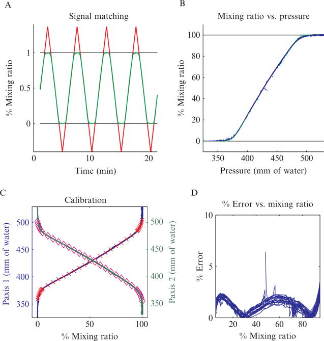
Performance of the DAW junction. (A) Calibration signal (red line) overlaid with output signal (green line) after correction for the delay in acquisition. During calibration the system is designed to intentionally overshoot the bounds of the DAW junction. Since the starting and ending points for calibration are not critical, this makes it easier to set up as described in the text. The ideal response would be a closely tracking output signal transitioning to plateaus after the system moves beyond 0% and 100% mixing ratios. As can be seen in the figure, this is what we observe, except for a slight rounding near the plateau region. (B) Compression of the data in part A into a single curve by mapping the input pressure directly to the output mixing ratio. Blue curve is the compressed data, while the green dots are the expected results from Comsol modeling. As can be seen in the figure, the modeling and experimental results are in excellent agreement. (C) Completed calibration for both inputs. Red crosses and pink diamonds represent polynomial fits of inputs 1 and 2, respectively, to the output mixing ratio. These fits can be used to program a linear actuator controller to generate precise inducer waves. (D) Measure of the percent error of the uncalibrated output signal, which general is less than 3%.
1.1.5. Calibration of the DAW junction
The junction is designed to be used in conjunction with linear actuators to physically move the input reservoirs up and down thereby altering their hydrostatic pressures. To map the height of the input 1 and 2 reservoirs to a mixing ratio of the DAW junction, we have come up with a simple calibration scheme. First we find two sets of reservoir heights corresponding to mixing ratios beyond 0% and 100%. Each set represents flow from one of the inputs being completely diverted into a shunt. Since the heights do not have to be exact at this step, it is relatively quick and easy to set up (unlike trying to find the exact 0% and 100% heights). Next we program the linear actuator controllers to generate a triangle input wave and begin to move the reservoirs. Generally we use an input wave with a 5-min period. We then monitor the fluorescence near the cell chamber to record the output signal. The two signals are overlaid and any delay is removed, as shown in Fig. 14.7A. In this figure, the input is shown in red and the output in green. We expect the output to closely track the input signal until a plateau is reached, indicating complete diversion of a inlet into a shunt. As can be seen in the figure, this is essentially what we see, with a slight rounding at skewed mixing ratios.
Once this mapping is complete we compress the data into a single curve, as shown in Fig. 14.7B. This figure depicts one of the external port pressures mapped to a mixing ratio of the DAW junction. An ideal response would be a plateau at 0% leading to a linear ramp until another plateau is reached at 100%. The output of our junction (blue curve) closely approximates this, again with slight rounding near 0% and 100% mixing ratios. As an additional example of Comsol’s utility, the green dots represent modeling results generated of the junction’s response. As can be seen in the figure, the modeling and experimental results are in excellent agreement. In Fig. 14.7C, the calibration results for each input are shown. A high order polynomial fit is used for each input, which can then be programmed into the linear actuator controller. Figure 14.7D represents the percent error of the output signal as a function of mixing ratio for the uncalibrated system. Even without calibration the system is highly accurate, usually having an error of less than 3%.
1.1.6. Design of an improved yeast cell trap
Beyond the flow network or DAW junction, the most important part of a microchemostat chip is the cell trap. Often a successful design will hinge on a properly functioning trap. A microchemostat’s cell trap should ideally be easy to load, force the cells to grow in a monolayer so they are all in the same focal plane, allow nutrients to enter the trap even when packed with cells, force cells to grow in well-defined directions to assist with cell tracking and allow cells to exit the trap without clogging the device. For some cell types, specifically mammalian cells, controlling the flow rate in the trap is also extremely important. We have found that even hearty mammalian cell lines, such as 3T3 cells, can be killed by extremely low flow rates (less than 1–5 μm/s). This requires the design of highly specialized traps to prevent any flow from reaching the cells after loading. We have never encountered an issue where yeast or E. coli cells seem adversely affected by flow, however the flow rate can be important for intercellular communication by diffusible substances (Danino et al., 2010).
Often the goals mentioned above are difficult to achieve completely, for example a trap with high cell retention is often very difficult to load. This is the case with the TμC chip described in Cookson et al. (2005). To overcome these problems, an improved yeast cell trap, known as the doughnut trap, was designed. Figure 14.4D and E contain an overview of this trap. The salient feature is improved loading while retaining the ability to image cells in a monolayer. Another major issue in the trapping region is clogging of cells from excess growth. Yeast cells grown in glucose can clog a device in several hours if the microchemostat is not properly designed. As shown in Fig. 14.4, the outer channel is designed with a height of 10 μm. This height is large enough that no cells will be able to clog it under normal circumstances. The height of the trap is kept at 3.525 μm for yeast cells of the W303 background. Note that the height of the trap is the most critical parameter of the entire chip as will be stressed in the fabrication section. Even height differences as little as 0.1 μm can make a difference in terms of the effectiveness of the trap. If the trap is too high, yeast cells will flow right through and not be trapped at all. Even those that are trapped may not grow in a monolayer and hence a uniform focal plane will be impossible to achieve. However, if the trap is too low, then it will be impossible to get the cells into the trap. Thus, the height of the trap depends intimately on the cell type and even the cell strain. We have noticed that some larger backgrounds of yeast actually require a slightly higher trap than other common laboratory yeast strains.
Upon loading, when cells flow into the chamber containing the trap, most will actually flow around the trap to the cell and shunt waste (port 3), since this region’s flow mostly goes around the trap. This is actually beneficial to the design since it allows growing cells to be quickly whisked away when they overgrow the trap, while minimizing any movements of the cells in the trap due to flow (which can make cell tracking difficult). Furthermore this difference in flow rates is primarily a consequence of the difference in the heights between the two regions. Recall Eq. (14.9) which states that resistance of a channel scales with the cube of the height. Thus while the height difference between the trap and the outer channel is only ~3 fold, the resistance difference will be ~27 fold.
Those cells entering the central channel will move to the base and become stuck at the entrance barrier. Since the trap height is slightly smaller than the diameter of a yeast cell, the cells cannot enter the trap without some assistance from the experimenter. Once enough cells have accumulated behind the entrance barrier, the experimenter will flick the microfluidic line attached to the cell port with his index finger. This perturbation will cause a momentary pressure disturbance which will force some cells under the barrier into the trap. Once in the trap they will be efficiently held between the roof of the trap and the glass cover slip.
During the course of the experiment, cells will divide and enter exponential growth. They will quickly fill up the trap and the colony will come into contact with its walls. The pressure exerted on the trap’s walls by the growing colony will generate a flow of cells, which can be modeled as a particulate flow (Mather et al., 2010). This flow will expel some cells from the trap into the outer channel, to be carried away into ports 4 and 5 (note port 5, originally the cell port now functions as a waste port). The design of the cell trap should take cell flow into account so it can be directed in appropriate ways. For example, to track cells often it is useful to direct their movement in a regular direction to limit the difficulty of tracking. With the doughnut trap, cell flow is directed in radial directions which works fairly well. However, we have been considering designing a new trap with internal baffles to limit lateral movements of the cells.
The MFD005a device has been used successfully to generate many types of input concentration waves for numerous yeast strains and genotypes. In general, the chip takes 1–2 h to set up and can run for several days depending on the conditions. The chip is highly useful for all types of small scale experiments involving dynamic environments. However, upon building this chip we realized that most of the time during an experiment our microscope sat idle between imaging frames. To make better use of our time and resources, we decided to build a parallel version of the MFD005a device which we have named the MDAW device.
1.2. A parallel DAW device
The parallel version of our MFD005a device was designed to have eight copies of the smaller device on a single larger device. This parallel architecture greatly increases the throughput of a run by allowing eight independent subexperiments to be conducted at a time. The utility of this design can be seen by comparing the number of ports required to carry out equivalent experiments for the progression of chip designs. With the Bennett chip, 64 ports are required to conduct eight experiments, for the MFD005a device, 40 ports are required, while the MDAW device requires only 26 ports. Since setup time is directly proportional to the number of ports a chip contains, this reduction represents a significant savings of both time and consumables. Of course designing such a device presents its own challenges, a major one being space. Since we wanted all features to fit entirely on a single 24 × 40 mm coverslip, space was at even more of a premium than with the MFD005a device.
To conserve space we compressed the features of the MFD005a device as much as possible while retaining functionality and maintaining a margin for fabrication errors. We made the device radially symmetric in order to provide equal resistance paths to the ports shared among the subexperiments. To divide the space, we separated the chip into eight circular sectors of equal area, similar to slices of a pizza. While a rectangularly shaped device would have been a better fit for the coverslip, it would have been more difficult to ensure the resistances were equal to the outlets for all subexperiments. Moreover excessive stage movement between locations during acquisition can generate bubbles in the microscopy oil. These bubbles sometimes show up after several hours into an experiment and can cause a severe loss of focus or degradation of image quality. To prevent these problems, the cell chambers were placed as close to each other as possible, which essentially requires radial symmetry. As an added bonus, this lowers the amount of time for stage movement between positions.
An overview of a MDAW subexperiment is shown in Fig. 14.8A. Compare this to the MFD005a device in Fig. 14.4A. Both contain a DAW junction, SHM features and a cell trap that are essentially identical, although the length of the channel between the DAW junction and the cell chamber has been reduced slightly in order to conserve space. In fact ports 1, 2, and 5 and the channels linking them are essentially equivalent to ports A, B, and C, respectively, in the MDAW device. The major difference is that ports 3 and 4 on MFD005a have been consolidated in the MDAW device. In the MDAW device, we call the port 3 analog the consolidated shunt port and the port 4 analog, the consolidated alternative outlet. The consolidated shunt port is connected to each subexperiment by an extensive collection network. This collection network can be seen in Fig. 14.9. To create this collection network, Comsol modeling was essential to ensure that the flows would be equal to their equivalents in the MFD005a device. This modeling indicated that the height of the collection network would have to be increased to 35 μm to sufficiently lower the resistance (shown in dark blue in Fig. 14.9). Moreover the shunt channels from the DAW junction now connect to the diversion channel before it reaches the consolidated shunt port, whereas in MFD005a they both reach port 3 independently. Comsol modeling indicated that back flow from the shunt into the diversion channel could be a problem if the diversion channel was not long enough. The connection point was extended to ensure this would not happen.
Figure 14.8.
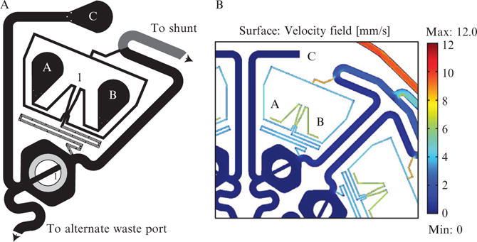
Graphic of the individual subexperiments in the MDAW microfluidic device. (A) This is a subexperiment from the MDAW device. It is essentially a compressed version of the MFD005a device shown in Fig. 14.4A. The ports labeled A, B, and C are equivalent to ports 1, 2, and 5, respectively, in Fig. 14.4A. The equivalents to port 3, the cell and shunt waste and port 4 the alternate outlet port, in the MFD005a device are shared among all eight subexperiments in this device. The arrows point to these shared ports. This port sharing reduces the number of outlets and eases the setup of such a large device. To make identification easier under the microscope, we have placed the subexperiment number above the DAW junction and near the cell trap. (B) Close-up of a Comsol model of the MDAW device. Comsol modeling was crucial for designing the combined collection network so each subexperiment’s shunt would function similar to the MFD005a device. Since the collection network combines the output of eight subexperiments, the resistance had to be lowered so it would carry the combined flow as efficiently as that in the MFD005a device.
Figure 14.9.
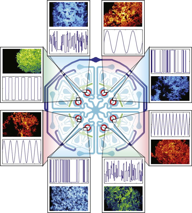
Graphic of the MDAW microchemostat device. The MDAW device has eight independent subexperiments. Each subexperiment can generate a separate inducer signal for an independent yeast strain. Examples of each are given in the breakout boxes. The system is capable of generating both periodic and pseudo random waves. The symmetry of the chip is important to ensure that all subexperiments have equal resistance outlet paths to the shared ports: the combined alternate outlet port (center) and the combined cell and shunt waste (top).
It was easier to consolidate port 4 into the alternate outlet port on the MDAW device since it was in the center of the chip and each subexperiment had an independent path to the port. Thus the height of these channels could remain 10 μm. However, the channel length between cell chamber and the alternate outlet port had to be reduced, which altered the resistance somewhat. Comsol modeling allowed us to determine the port pressures which led to equivalent flow. One might wonder how many ports could be shared among a device of this size. Of course if a multilayer microfluidic device were used then there would be no restriction; however, we believe the time required to manufacture multilayer devices does not justify their added benefits and therefore we avoid their use if possible. For a single layer device, at most two ports can be shared among all subexperiments due to geometric constraints. It is possible to share additional ports between adjacent subexperiments, however, with the MDAW device this would have meant sharing the cell ports (port C) and we wished them to remain independent. It is also possible to add y-junctions or manifolds to connect multiple outlet ports to a single reservoir. However if this is done, extra care must be taken to ensure no bubbles are introduced in the lines. This is especially a problem with small diameter y-junctions.
Even at eight subexperiments you begin to push the limit of what modern microscopes can accomplish. For example, on our current setup using the Nikon TI, the amount of time it takes to autofocus, change filter cubes, acquire a phase contrast image and 2–4 fluorescence channels and move stage positions for eight subexperiments is nearly 1 min. Since phase contrast images must be taken approximately every minute for adequate cell tracking, the microscopy setup becomes limiting before the microfluidics. While laser based focus systems would offer an increase in speed, many, like the Nikon Perfect Focus System, do not work well with PDMS devices. Thus while other microfluidic devices have been produced which offer a far greater number of independent experiments, often they cannot track individual cells due to excessive movement between frames (Taylor et al., 2009). This prevents the acquisition of cell trajectories and the device essentially functions similar to a highly parallel flow cytometer. Thus the device chosen should reflect the type of study and data required. For generating large numbers of cell trajectories in a dynamic environment with relative ease of setup, our device works well. For generating population level data using an extremely large set of conditions the device described in Taylor et al. (2009) would be superior.
1.3. Cell tracking
For microchemostat experiments cell tracking is essential for capturing high quality data. In fact, one could argue that effective cell tracking is as important as the design of a microfluidic device itself. Like a high powered computer running an early version of DOS, even the best device is not much use if the cells cannot be tracked. Thus most articles making use of microchemostats make a reference to “custom Matlab code” used for cell tracking (Bennett et al., 2008; Hersen et al., 2008; Kurth et al., 2008; Lee et al., 2008; Taylor et al., 2009). Our lab is no different and we have spent much time and effort generating a software package which works quite well but has room for improvement. There is also a program called CellTracer available free online (http://www.stat.duke.edu/research/software/west/celltracer/). It should be stressed that a microchemostat should be designed with cell tracking in mind from the beginning, rather than designing software to track how the cells happen to grow in the device. For example, by making the cell culture expand in defined, regular directions the cell tracking routine becomes less complex and hence works better. An excellent example of this concept is the trap described in Rowat et al. (2009) which constrains yeast cells in essentially one dimension and makes lineage tracking quite robust.
The essential problem for tracking all types of cells, and yeast cells are no exception, is that they simply are not unique, at least as viewed under phase contrast microscopy. This can be seen in Fig. 14.10 which compares different parameter values for a population of cells. Ideally each cell would occupy a unique position in some high dimensional space, corresponding to a combination of parameters, such as cell area, eccentricity, and fluorescence, specific for that cell and invariant in time. This would be similar to a bar code or serial number for cells. However, as seen in Fig. 14.10 there is simply no combination of inherent characteristics visible under this type of imaging which can uniquely identify all members of the population at once. If there were, there would be no clusters of high density in the histogram. Moreover, since cells grow and divide, there is often a high amount of variability in the geometric properties between frames for the same cell. Unfortunately the only parameter which is unique for all cells confined to a monolayer is position. Thus it is of critical importance to keep track of cellular position during a microchemostat experiment and this explains why phase contrast images must be taken frequently. For fast growing cell types such as yeast or E. coli, frequent sampling is a necessity. If the cellular movement is greater than one cell diameter between frames, cell tracking becomes next to impossible.
Figure 14.10.
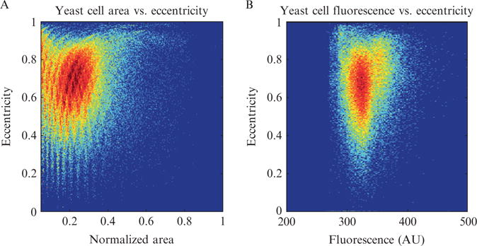
Comparison of different cell parameters for a population of yeast cells. (A) Two dimensional histogram of yeast cell eccentricity versus area. Striations in the data are a remnant of the ellipse filter used to segment the cellular boundaries. Notice that most cells have similar values for eccentricity and area. (B) Similar plot as part A, except here eccentricity and mean fluorescence are plotted.
Cell tracking software can be divided into two basic types, segmentation based methods and nonsegmentation based methods (Miura, 2005; Mosig et al., 2009). Segmentation methods are the more common type and will be the focus of this discussion. In a segmentation method, a transmitted light image of the cell population is converted to a binary image containing only the outlines of cells. This is repeated for each image of the experiment and trajectories are formed by linking cellular objects between frames based on shared characteristics. Binary images are preferred since there are a large number of mathematical functions available for processing them. To convert a transmitted light image to a binary image the simplest method to use is a threshold. Essentially anything below the threshold is converted to black and anything above to white. Phase contrast images typically have a light halo around the boundary of cells, which provides high contrast, and thus are perfect for thresholding. A comparison of phase contrast imaging to differential interference contrast imaging, which is less suitable for thresholding, is shown in Fig. 14.11.
Figure 14.11.
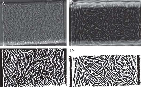
Comparison of phase contrast and differential interference contrast (DIC) imaging with regards to cell tracking. (A) DIC image of an E. coli colony growing in a microchemostat device. (B) Phase contrast imaging of a similarly grown E. coli colony. (C) Binary image created by thresholding the DIC image shown in part A. Notice how difficult it is to distinguish the cellular boundaries. (D) Thresholded version of the phase contrast image in part B. Notice how much more clearly the cellular boundaries are compared to C.
Typically a threshold value will be chosen to retain the boundary halo while discarding all other features, thus preserving only the boundary of cells. This procedure works fairly well assuming there are no other “phase objects” present in the cell. Unfortunately, yeast vacuoles are quite prominent under phase contrast microscopy and often are difficult to remove by thresholding alone. This necessitates later postprocessing steps to remove the vacuolar artifacts to prevent errors in segmentation. Some yeast backgrounds or mutants can have especially prominent vacuoles which can be problematic. Moreover, environmental conditions, stress and aging can increase vacuole prominence. Thresholding based segmentation routines will need to cope with vacuoles and this is a downside of the technique for yeast. In spite of these issues, thresholding usually works well enough to be a reliable first step of the tracking procedure when chosen appropriately.
After thresholding the cellular boundaries are generally prominent but incomplete. Due to the aforementioned vacuole problems, often an aggressive threshold value is chosen leaving only the most prominent features of the image. While more successful in removing vacuolar artifacts, this will also remove some the cell’s boundaries. For efficient processing of binary images, the image must be composed of only completely closed objects. Thus any cells lacking completely closed boundaries will not be found by the algorithm. Even if vacuoles are not a problem, a morphological closing operation is performed to repair inevitable boundary defects. This closing operation is done using either a structuring element or the watershed algorithm. Structuring elements are small geometrical objects which can reinforce common motifs of the image. We have found them to be very useful for processing E. coli cells.
Implemented in ImageJ and Matlab, the watershed algorithm is good at repairing small defects in cellular boundaries. However, if even a small vacuolar remanent remains, the watershed algorithm will bisect the cell through it, causing improper segmentation. An example of how the watershed algorithm performs in segmentation is given in Fig. 14.12. Note that another thresholding tradeoff comes from deciding how much to emphasize cells at the edge versus those in the interior of a microchemostat’s colony. Multiple cells in close contact reinforce their boundary halo’s, causing the signal from these areas to be greater than from isolated cells at the edge of the colony. When choosing a threshold value that maximizes boundaries and minimizes vacuoles, often the boundaries of cells on the colony edges are removed. This can be seen in Fig. 14.12. These boundary cells are consequently often dropped from the segmented image.
Figure 14.12.
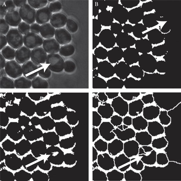
Segmentation of yeast phase contrast imagery (A). Phase contrast image of a tightly packed yeast cell colony. The white arrow points to a cell with a prominent vacuole. (B). Binary image created by thresholding the image from part A. The thresholding value was chosen to minimize vacuolar artifacts, but also has the effect of removing boundaries of cells on the colonies edge. The white arrow points to a cell with a deficient boundary. This cell will not be closed by the watershed algorithm and therefore will not be present in the segmented image. (C) Binary image created by thresholding A with a less stringent cutoff value. Notice that the boundaries are thicker and well defined, but that the vacuoles are more prominent than B. White arrow points to a vacuolar artifact. (D) Segmented image made from performing the watershed algorithm on the thresholded image from part C. Note that the vacuolar artifact has caused the segmented cell to be split into three regions. In later processing steps each of these regions will be considered cells, thus potentially causing errors in tracking.
After segmentation the binary image is processed to extract useful data from the contained objects. To assist in this processing, we fit each object to an ellipse since we have found that it generates a good approximation to a yeast cell’s shape. After processing each image in an experiment we link cells between images to form trajectories. To accomplish this we have a scoring function which compares two cells and generates a score based on how likely they are to be the same cell. We compare the position, area, eccentricity, and orientation of each pair of cells to be scored. While we could also use the fluorescence values of the cell, we have found that this usually does not improve the score’s power and often is not possible since we take phase contrast more often than fluorescence images. The scoring of cells between frames is usually the most computationally intensive part of the entire process. To aid in the computation we only compute scores for cells in the same general location of the two images, since if the cells have moved more than one cell diameter between frames they become virtually impossible to track anyways. This greatly reduces the computational time. Images of the MFD005a and MDAW traps generally contain ~1000 cells when fully packed; runs sampled every minute for 2–3 days will have thousands of phase contrast images to process. Clearly, any savings in time are important.
After scoring we remove cells which are below a threshold empirically determined to result in a poor match. To match a cell from the current frame to one from a previous frame there are several cases which need to be dealt with. These cases are depicted in Fig. 14.13. The first is the easiest which is a unique match between a cell from frame n and a cell from frame n − 1. In this case, the cell from frame n is assigned to the n − 1 cell’s trajectory. An example of our algorithm’s scoring output for the single match case is given in Table 14.5. The next case is when two cells match to the same trajectory. This often happens due to excessive cell movement and the cellular position becomes a less powerful discriminant. In this case, the cell with the highest score will be retained as the trajectory’s match and the other cell will be moved to its next highest scoring trajectory. The third case is a skip, where a trajectory was present in frame n − 2 but for whatever reason a match was not found in frame n − 1. This often happens due to a segmentation error in frame n − 1.
Figure 14.13.
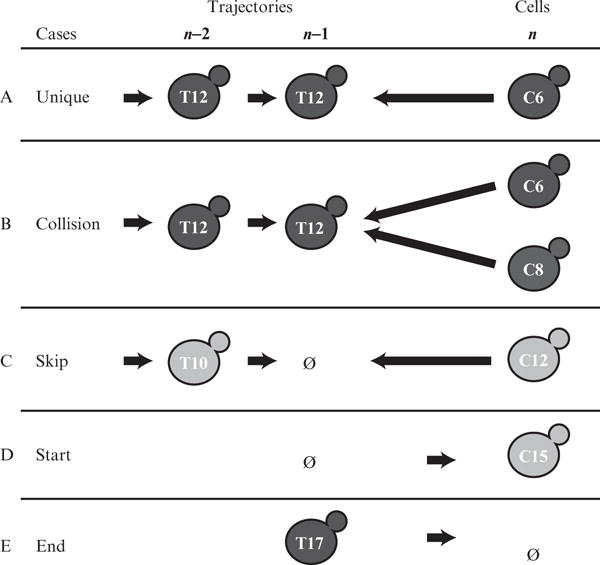
Different cases which need to be handled in cell tracking. Each case is given on the left hand side of the figure. The cells representing trajectories present in frames n − 2 and n − 1 are given in the middle portion of the figure. These cells are labeled with their trajectory number (e.g., T12). Cells in the current frame (n) are shown on the right hand side of the figure. They are labeled with their cell number (e.g., C6). (A) Unique match. A trajectory present in the previous two frames matches a single cell in the current frame. (B) Collision. Two cells have the same trajectory as their best match. Normally the highest scoring cell is chosen as the match; however, this is a symptom of poorly acquired data (cells have moved too much between frames) and will likely lead to mistakes. (C) Frame skipping. A trajectory present in frame n − 2 did not find a match in frame n − 1 but does find a match in frame n. This often is caused by segmentation errors in the n − 1 frame, especially vacuolar splitting of cells (see Fig. 14.12D). If this case is handled, longer trajectories can be generated, however there is a potential for the algorithm to become overly greedy. (D) Start of a trajectory. A cell is either born or moves into the frame. (E) End of a trajectory. A cell either dies of moves out of the frame.
Table 14.5.
Sample yeast cell tracking output
| Trajectory 36 | Base | Predicted | Cells | |||
|---|---|---|---|---|---|---|
| Score | 0.1 | 2.1 | 2.5 | 2.5 | ||
| Area | 871.0 | 871.0 | 856.0 | 615.0 | 608.0 | 560.0 |
| CentroidX | 592.4 | 591.1 | 591.3 | 605.1 | 575.3 | 572.2 |
| CentroidY | 596.2 | 602.6 | 599.1 | 630.9 | 566.9 | 631.0 |
| Eccentricity | 0.5 | 0.5 | 0.5 | 0.5 | 0.8 | 0.5 |
| Orientation | 63.0° | 63.0° | 50.8° | 71.7° | 51.2° | −53.3° |
| Object | 610 | NaN | 621 | 640 | 603 | 601 |
| Fluor mean | NaN | NaN | 392.6 | 331.2 | 390.3 | 326.4 |
| Fluor std. | NaN | NaN | 603.4 | 316.3 | 538.5 | 277.2 |
Comparison of a cell from a given trajectory and the nearest cells in the next frame. The data for the trajectory is taken from its matched cell in the previous frame. This is called the base cell. The predicted column refers to the algorithm’s prediction of how the cell’s properties should have changed in the current frame based on its previous behavior. This prediction is usually generated from MatPIV data of the colonies movement. While not shown here, it is also possible to predict a change in area from previous growth data. Note that a lower score is better and all scores above 1 are considered to be below the scoring threshold and thusly discarded.
If vacuoles are prominent, this type of skipping may happen often and should be corrected for. By keeping trajectories for an extra frame you can match a cell from frame n to a cell from frame n − 2. The next case is the start of a trajectory. Here a new cell is formed. The last case is the removal of a trajectory, here the cell either left the field of view or died. One has to be careful that the algorithm is not too “greedy” by always finding a match for a cell in the previous frame. Cells are born and cells die, these events will happen and if an algorithm is too greedy it will end up making improper trajectories. For example, often a greedy algorithm will cause a trajectory, which should have ended due to a cell leaving the trap, to jump to an adjacent trajectory. This is sometimes worse than ending a trajectory prematurely because it can be difficult to detect unless one goes through the data very carefully. Thus to obtain long, reliable trajectories one needs above all else good data and an algorithm which is balanced among all cases.
To reliably link cells into trajectories the number of cells uniquely matching a trajectory should be maximized. As stated earlier, the largest impediment to unique matching is movement of cells as the colony expands. This can be severe for E. coli or even yeast grown in rich media. In fact, sometimes it is possible to see movement of the colony due to growth in real time under high magnification. To correct for bulk movements of cells a particle image velocity (PIV) program can be invaluable. PIV programs are imaging analysis routines which are able to detect particulate flows in a sequence of images by comparing how the field of view changes in time. This is very useful for tracking bulk movements of cells and can often significantly improve the fidelity of tracking. We use a program called MatPIV, which has been conveniently implemented in Matlab, to track cell flow in our images (Sveen, 2004). Using this data we come up with a predicted position for each trajectory present in frame n − 1 for frame n. An example of how this is useful is shown in Fig. 14.14. The MatPIV generated velocity field has been used to adjust the position of the cells resulting in more robust tracking.
Figure 14.14.
Overview of the cell tracking process. (A) Raw data: phase contrast image of yeast cells. Note the high contrast between the boundary of the cell and the exterior. (B) Segmented image after thresholding, application of the watershed algorithm and fitting the resultant objects to ellipses. (C) Scoring of a cell from frame n (shown in red) to trajectories present in frame n − 1. Lower score is better. Notice that the red cell has closely overlapped with a previous trajectory and generates a better score. All other scored cells are above the scoring threshold (which is set at 1). Note that the scoring system here has generated good contrast between the ideal match and the neighbors. This is indicative of a good match. (D) Colored image of the masks after trajectory finding is complete. Colored regions represent trajectories which are numbered. (E) Overlay of the trajectory image from part D with the phase contrast image of part A. Note most cells were assigned trajectories except for smaller cells and cells near the exterior. (F) Example of MatPIV processing for cell flow. White arrows indicating the cell flow velocity are overlaid with a phase contrast image of the colony. (G) Image of cells from frame n − 1 (opaquely colored objects) overlaid with cells from frame n (translucent objects). Notice there is an overall movement of cells toward the lower left corner of the image due to cell flow. Also note that the distance traveled here is almost one half cell diameter between frames for some cells. One can see how this movement could generate ambiguous situations for similarly shaped cells without prior knowledge of the cell flow. (H) Same cell field as in part G except MatPIV velocity information has been applied to correct for cell flow. Notice the much better overlap compared to part G. This will lead to more reliable matches since cell position is crucial for reliable matching.
In principle, the change in a cell’s area and eccentricity could also be predicted from previous data. These changes would be most pronounced for newer, smaller cells. However, we have not done this and it is unlikely to improve tracking appreciably. An overview of the entire procedure is given in Fig. 14.14. The overall sequence of events is presented in the figure. We have done much work to improve the visualization of the trajectory data to ensure high quality. While the linking of trajectories works very well, the biggest improvements can be made in the segmentation steps of the process. Indeed, some cell tracking methods have no segmentation step at all, relying on comparison based methods for identifying cells in an image field (Miura, 2005). These methods generally rely on comparing a reference library of known cells to the current image using a cross-correlation function. The cross-correlation function will be maximized when the reference image matches a cell in the target image. Indeed, MatPIV works in a very similar way for tracking cell flows.
In principle, comparison methods could get around the vacuole problems mentioned above which are the bane of the segmentation approach for yeast. However, comparison methods can have problems if the cells change markedly between frames, which will happen due to growth, division and rotation. While there are ways to correct for this, in general, they are computationally intensive. In fact, the whole process is much more computationally intensive than the segmentation method. We are currently working on a hybrid method which employs an initial segmentation step that is corrected using a comparison step. Since segmentation works quite well, running it initially will reduce the space to be searched by direct comparison. The subsequent comparison step will correct for any initial errors in segmentation. Fortunately, cross-correlation methods lend themselves to parallel processing, and modern graphics cards can be programmed to greatly speed up computation (Owens et al., 2008). In the future, we expect more use of parallel processing and comparison based methods for cell tracking. However, it should be emphasized that no matter how well designed an algorithm is, the most crucial determinants for success are the quality of the initial data and the regularity of a cell colony’s movements.
1.4. DAW hardware and software
1.4.1. Hardware
As mentioned in the chips design section (1.1.3) of this chapter, the DAW junction works by changing the relative pressures at DAW ports, while keeping the total pressure the same. Physically this can be achieved in a number of ways: by pneumatically pressurizing the syringes, using a syringe pump, or changing the hydrostatic pressures of the syringes. Our initial design relied on pneumatically pressurized syringes, but due to problems with flow control we switched to a hydrostatic system. We use two vertically mounted linear actuators to change heights of liquid filled syringes that feed into the DAW junction, Fig. 14.15A. The smooth motion of the linear actuators allows for smooth changes in mixing ratios. Linear actuators are also a better solution in case of a hardware malfunction. If the actuators break down or cannot move to a new position, they will still allow the experiment to continue, since the flow depends only on the position of the syringe. The inability to move the syringes will only result in a constant inducer level, while maintaining a steady flow. In case of a malfunction with syringe pump or pneumatically driven system the flows will change over time and might even result in flow reversal, which would most likely ruin the experiment.
Figure 14.15.
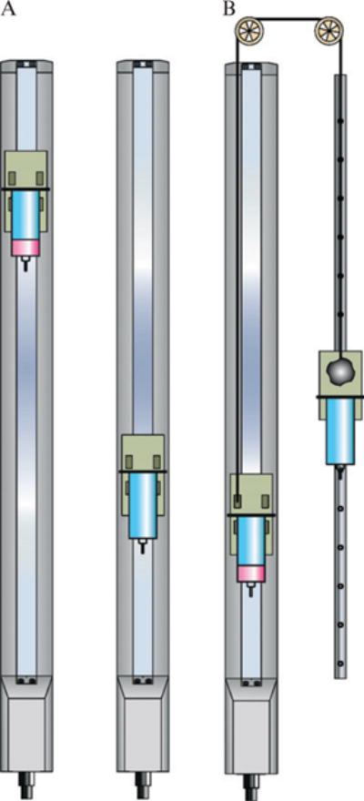
Linear actuator setup for DAW. (A) Dual linear actuator setup. Each actuator can be move individually. One of the actuators (left) moves a media syringe with added dye. (B) Alternate design of the DAW system using only a single linear actuator. The actuator controls the position of both syringes simultaneously. To eliminate friction in the system the following components need to be in a single plane in space: both pulleys, line attachment to actuator, and line attachment to linear guide block.
The first version of DAW system had two linear actuators, which could be controlled independently, Fig. 14.15A. By attaching a syringe with media to each actuator and moving them equal distances in opposite directions we were able to change the ratio of pressures at the DAW ports while keeping the total pressure constant. Since we have constrained our total pressure to be constant, the movement of one actuator has to be mirrored by the movement of other actuator in opposite direction. In essence, the second linear actuator could be replaced with a linear guide and a pulley system, as seen in Fig. 14.15B. The linear guide consists of a rail and a guide block that slides along the rail. We found that the guide block does not have enough mass to keep a taught line through the pulley system. A steel block was used to weigh down the guide. Also, the length of the line between the linear actuator cart and the guide block needs to be adjustable. This can be achieved by attaching the line to guide block with a pinch mechanism operated by a screw.
The elimination of the second linear actuator proved to have a major benefit of reduced setup cost per DAW unit. However, when considering the additional parts and labor required to fabricate a pulley system the value of this benefit diminishes. Unless you intend on running a full eight trap MDAW chip, we recommend on installing a dual linear actuator system. During installation the actuators should be securely attached to some sort of a support system. In our case, we attached them to metal struts that are directly connected to the wall studs.
From Table 14.6, which lists all the required parts for a dual linear actuator system, we can see that there are two linear actuator controllers (RPCON) and a single communication gateway (SIO) module. The SIO module is used for communication to a computer, while the RPCON’s connect the actuators to the SIO. This setup seems redundant, but it allows for easy expansion. The SIO module can operate up to 16 individual linear actuators, while maintaining only a single connection to the computer. Using this system from the start will allow one to easily expand from 2 to 8 axis DAW system. Also the SIO can be wired to communicate with a computer via USB interface.
Table 14.6.
Hardware required for DAW actuator setup
| Equipment | Qty | Part No. | Vendor |
|---|---|---|---|
| Linear actuator: fast speed, 800 mm travel length | 2 | RCP2-SA7C-I-56P-16-800-P1-M-BE | Valin Corp. |
| Controller | 2 | RPCON-56P | Valin Corp. |
| Communication gateway module | 1 | RGW-SIO | Valin Corp. |
| Serial communication cable | 1 | CB-RCA-SIO-050 | Valin Corp. |
| USB adapter | 1 | RCB-CV-USB | Valin Corp. |
| USB cable | 1 | CB-SEL-USB010 | Valin Corp. |
| 24V DC power supply | 1 | OMRON-S8VS-06024 | Valin Corp. |
| AC power cable | 1 | 70355K34 | McMaster-Carr |
1.4.2. Software: iDAW
To control the linear actuators we have created a custom software, nicknamed iDAW, using the National Instruments LabVIEW environment. Currently there are two major versions of the software, for the 2- and 8-actuator systems. Both versions, manuals and installation guides are freely available by request.
The graphical user interface presents the user with three main areas: actuator controls, calibration, and experiment setup as seen in Fig. 14.16. During a typical experiment, the actuators first have to be calibrated to the specific chip. This calibration establishes a relationship between relative positions of each actuator and the respective mixing ratios. There are two ways to calibrate the system: manually and automatically. The automatic calibration was already discussed in an earlier section. During manual calibration the actuator positions are changed to create different mixing ratios. Once all the calibration points have been acquired the software creates a calibration function. The software allows up to 11 calibration points, but we have found that a two point calibration performs very well. Also, depending on the number of points, the order of the calibration function can be increased for improved data fit.
Figure 14.16.
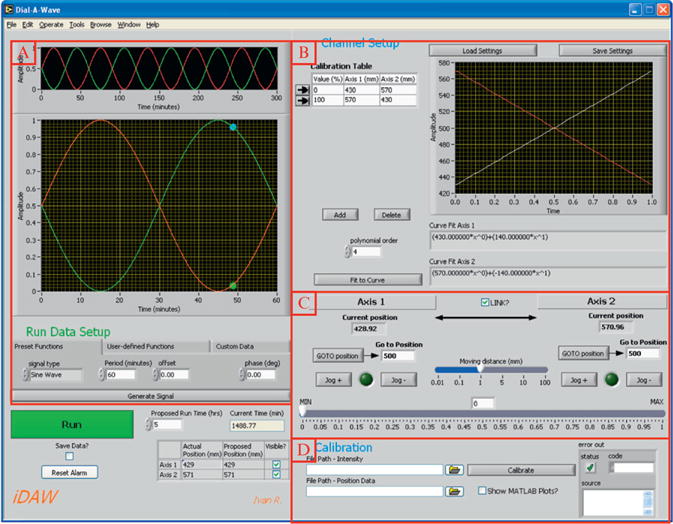
Screenshot of iDAW software. (A) Experimental parameter setup allows user to set up mixing ratios as a function of time. Most mathematical functions or an arbitrary dataset can be used as templates. (B) Manual calibration. The table records the calibration points and the graph shows the calibration functions. In this example, a two point calibration was used to create a linear calibration profile. (C) Actuator controls allow the actuators to be moved independently or together when in “Linked” mode. (D) Automatic calibration functions take position data from the actuators and fluorescence data from the microscope to determine the calibration profiles.
To start the manual calibration procedure the actuators are moved together to a height that provides the desired flow to the cell trap. Since the pressures at both syringes are the same, this becomes the 50% value for the calibration. Next, the actuators are linked to move equal distances in opposite directions. The positions are adjusted until there is only media with the inducer going through the mixer, this becomes the 100% point. Similarly, the 0% point is recorded. The 0% and the 100% points are used to make a linear calibration function as can be see on the graph in Fig. 14.16B.
The experimental setup area of iDAW allows the user to create a profile of induction versus time. The user can choose from a number of built-in functions, such as square or sine waves, or load an arbitrary function. The software automatically adjusts the inducer values to fit between 0% and 100%. The proposed induction profile is plotted for the duration of the whole run and the individual linear actuator positions are constantly updated, Fig. 14.16A. These displays eliminate errors during experimental setup and actual run-time.
2. Part II: Fabrication
With the design of the chip drafted and thoroughly analyzed we begin the fabrication process. An overview of fabrication is shown in Fig. 14.17. The complete fabrication of a microfluidic chip can be broken down into three main phases. In the first phase we create a patterned wafer by photolithography. Next, we use this wafer to create a silicon rubber mold by a process of soft lithography. And finally the silicon is prepped and bonded to a glass coverslip to make a functional microfluidic device.
Figure 14.17.
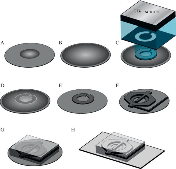
Overview of the fabrication process. Photolithography (A–F), soft lithography (G), and PDMS processing (H). (A) Photoresist deposition. (B) Spin coating: the deposited photoresist is spun at a specific speed to create a uniformly thick layer. (C) UV exposure cross-links the photoresist creating a pattern identical to the photomask. (D) Postexposure baking joins the silicon wafer and the cross-linked photoresist. (E) Developing removes the uncross-linked photoresist, revealing the features. (F) Repeating steps A–E creates additional features. (G) Pouring and curing PDMS over the patterned wafer creates a mold. (H) Bonding the PDMS mold to a glass coverslip finishes a microfludic chip.
2.1. Photolithography
Photolithography was initially developed for the semiconductor industry and later applied to a variety of fields, including microfluidics (Xia and Whitesides, 1998). The process relies on transfer of a geometrical pattern from a mask onto a photosensitive layer via light radiation. The first step involves thorough cleaning of the wafer, which will act as the foundation for all the features. It is very important to remove all debris and any chemicals from the surface of the wafer, as they will get incorporated into the final wafer design and will highly affect the adhesion properties of photoresist to the wafer. Next, we deposit a small amount of photoresist onto the wafer and spin the wafer at predetermined speed to create a photoresist film of precise height, this step is called spin coating. The wafer is then soft-baked by gradual heating on a level hot plate, which removes solvent and enhances photoresist adhesion to the wafer. At this point the wafer is exposed to UV light through a photomask, this transfers the pattern from the mask onto the photoresist layer. We use the SU-8 2000 line of photoresist from Micro-Chem Corporation. SU-8 is a negative photoresist, which means that areas of the film exposed to UV radiation will form solid structures, while unexposed areas will be washed away during the developing step. The wafer is then baked again, in the postexposure bake (PEB), to increase the level of cross-linking. And finally to complete a single photolithographic cycle, the wafer is developed by immersion in solvent which removes uncross-linked photoresist leaving only the desired pattern on the wafer. Since all of the chip designs we use require wafers with multiple heights this cycle is repeated a number of times.
2.1.1. Photoresist
Manufacturers, such as MicroChem, make a variety of photoresist formulations. The SU-8 line of resists alone has three subcategories with a total of 18 different formulations, specific for heights ranging from 1.5 to 550 μm (MicroChem, 2010). We use the SU-8 2000 photoresists which have great adhesion to silicon wafers and are able to make high aspect ratio structures (del Campo and Greiner, 2007). The “negative” denomination of a photoresist means that areas of the film exposed to UV radiation will form solid structures, while unexposed areas will be washed away during the developing step. Specifically exposure to UV radiation changes the chemistry of the resist by generating a very strong acid within the film, which starts the cross-linking reaction of the SU-8 epoxy. The main difference between the various SU-8 2000 formulations is the epoxy solids content that directly relates to the viscosity of the liquid as can be seen in Table 14.7.
Table 14.7.
SU-8 2000 photoresists formulations
| SU-8 2000 | % Solids | Viscosity (cSt) |
|---|---|---|
| 2000.5 | 14.3 | 2.49 |
| 2002 | 29.00 | 7.5 |
| 2005 | 45.00 | 45 |
| 2007 | 52.50 | 140 |
| 2010 | 58.00 | 380 |
| 2015 | 63.45 | 1250 |
| 2025 | 68.55 | 4500 |
| 2035 | 69.95 | 7000 |
| 2050 | 71.65 | 12,900 |
| 2075 | 73.45 | 22,000 |
| 2100 | 75.00 | 45,000 |
| 2150 | 76.75 | 80,000 |
Commonly there is a need for a nonstandard formulation. It is possible to make new, less viscous, formulations by adding SU-8 thinner to the initial, more viscous, stock of photoresist. It should be noted that the manufacturer’s naming scheme loosely relates to the height of the photoresist film when it is spun at 3000 rpm. Thus, for 2002 and 2005 photoresists, spin coating at 3000 rpm would in theory produce 2 and 5 μm film heights, respectively. Using this information we can plot these theoretical heights against the percentage of solids for each formulation, as seen in Fig. 14.18. By making a curve fit function of percent solids (s) as a function of height (h), as written in Eq. (14.33), we are able to estimate the required solids for any new formulation. For example, to make a new formulation, which would produce 3 μm height at 3000 rpm, we use Eq. (14.33) to determine that it requires 35% solids
| (14.33) |
Figure 14.18.
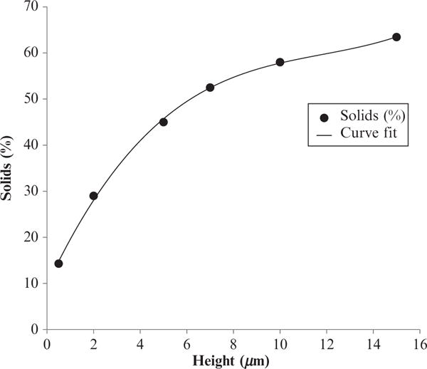
Graph of SU-8 formulation versus percent solids. Relationship between estimated height of SU-8 formulations when spun at 3000 rpm and their solids content.
Next, the amount of thinner required for the new formulation can be calculated using the relationship described in Eqs. (14.34a) and (14.34b), where masstotal is the desired mass of the new formulation, massthinner is the required mass of thinner, massinitial is the required mass of original photoresist, sinitial is the percentage of solids in the original photoresist, and sfinal is the percentage of solids in the desired photoresist formulation.
To make the formulation measure out and deposit the predetermined amounts of photoresist and thinner into a clean amber glass bottle, make sure to do this in a fume hood. Drop a clean stir bar into the bottle and place on a magnetic stirrer, until it is thoroughly mixed. Due to the viscosity of photoresists removing the stir bar could be difficult, so we leave it in the bottle until the photoresist runs out
| (14.34a) |
| (14.34b) |
Finally, to complete the process it is necessary to characterize the new photoresist formulation by making a spin speed curve. This step should also be performed for any standard formulations that have not been previously characterized by your lab. To create a spin speed curve for a particular photoresist the photolithographic cycle, described later on, should be repeated 3–6 times with various spin-coating speeds. For each speed, measure and record the feature heights using a surface profilometer. Plotting and curve fitting the data will produce enough data to reliably estimate spin speeds for specific heights. As mentioned earlier, the functionality of a cell trap is dependent on its height. Thus, it is critical to manufacture the exact height required by the design. The spin curves allow us to estimate only a rough range of speeds required to achieve a height. Using this range as a starting point, we perform as many spin test as necessary to get the desired height. An example of an actual spin curve for 2003 formulation can be seen in Fig. 14.19. Examining the figure it becomes evident, that our 2003 formulation produces 2.6 and not 3 μm height at 3000 rpm, this fact reinforces the need for photoresist characterization.
Figure 14.19.
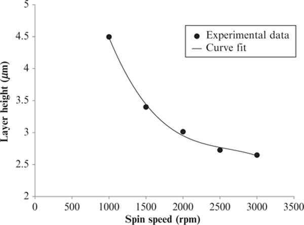
Example spin curve for an SU-8 2003 formulation. As spin speed increases the the spun photoresist thickness decreases. The graph levels off at high speeds, with further increases in spin speed having little effect on layer thickness.
2.1.2. Equipment and environment
Due to sensitivity of photolithography to contamination it is usually performed in a cleanroom environment. A number of universities and research centers have shared facilities that house equipment necessary for photolithography and other dust-sensitive processes. We have made wafers in various environments from a Class 100 cleanroom to a basic HEPA filtered room with no rating. The latter type of noncleanroom manufacturing environment is achieved by creating a dedicated fabrication space, installing HEPA filters over the air ducts and changing the ceiling panels to nonparticulate releasing tiles. Also to prevent uncontrolled photoresist cross-linking, the lights should be fitted with UV absorbing filters. This can be easily done by placing thin filter sleeves over the fluorescent lights bulbs. Although it is beneficial to carry out the whole manufacturing process in the cleanest possible environment, in our case only photolithography is performed in the cleanroom. While soft lithography and PDMS processing are carried out in regular lab space.
It is important to point out that the chemical safety precautions are more important than the cleanliness of the facility. Some of the chemicals used in photolithography are potentially carcinogenic, labs should use a properly functioning fume hood when working with photoresists and developers at all times. A standard fume hood convects air from the environment past the user, into the hood and out a ventilation shaft. Since users are generally the largest source of particulates in a clean environment, use of a standard fume hood can increase the local concentration of particulates over the work surface in the hood, even if the surrounding environment is clean. In contrast, biosafety cabinets contain a laminar air stream between the interior and the user, preventing the transfer of particulates into the hood. However, unless specially made and calibrated, biosafety cabinets can potentially allow chemical fumes to escape into the work area. Purpose built hoods, protecting both the user from chemical fumes and the interior from particulates, do exist but are expensive. For microchemostat fabrication, we have found that a standard chemical fume hood is sufficient; however, electrical engineering facilities will often contain specialty hoods. Since hot plates and spin processors are used with uncured photoresists, it is essential that they be placed in the fume hood. However, the process of soft-baking removes the solvent from photoresist, allowing one to work with a mask aligner outside of the fume hood.
2.1.3. Photomasks
Conventional photolithography requires expensive chrome photomasks, we use the cheaper photomasks printed on a transparency-like material as described in Whitesides et al. (2001b). As mentioned earlier, all of our masks are made by CAD/Art Services, Inc. (Bandon, Oregon). They use a photographic process to print the design on a 0.007″ polyester mylar sheet coated with photographic silver. Since our masks are designed in AutoCAD software, we just provide them with a *.dxf file. However, they do accept a variety of other CAD files, listed in order of preference: *.dwg, *gds, *.cif, *.gerber, and *.eps. Due to the limits of their photoplotting process, the minimum feature size is defined by a circle with 10 μm diameter. Although, it is possible to print various size masks, we usually order an 8 × 10-in. sheet. This gives us enough room to fit up to six individual layer masks and since most of our design require less than six layers we can have a whole chip printed on a single sheet. When ordering the mask, it is important to specify the polarity of the mask, considering that we are working with a negative photoresist, our masks need to have clear features on a black background. Once the masks have been printed, they are cut out and individually glued at the corners to a 3 × 3-in. glass square using clear instant adhesive. It is important to have the emulsion side of the mask facing away from the glass, since it needs to be in contact with the photoresist later on. Also, when gluing the photomask to the glass make sure to keep the glue away from any transparent parts of the mask. For storage and transport we keep the masks in individual plastic bags, this prevents them from getting dirty and scratched.
2.1.4. Sample fabrication parameters
For each individual wafer we create a table with fabrication parameters, this is an effective way of condensing all of the necessary information for manufacturing the wafer. Most of the parameters, such as layer heights and number of layers, will be dictated by your design, however some of them have to be calculated after the design is done. For example, the exposure time will depend on the exposure dose required for the photoresist and on the UV lamp power. MicroChem’s datasheets provide exposure energy ranges for different heights. For example, 0.4 μm layer requires 60–80 mJ·cm−2 and 3 μm layer requires 90–105 mJ·cm−2. Given that our mask aligner UV lamp has an effective power of 1.4 mJ·cm−2, we can calculate the exposure times using Eq. (14.35), see Table 14.8.
Table 14.8.
Calculated and experimental exposure times
| Layer height (μm) | Exposure energy (mJ/cm2) | Calculated exposure time (s) | Experimental exposure time (s) |
|---|---|---|---|
| 0.4 | 60–80 | 43–57 | 60 |
| 3 | 90–105 | 64–75 | 80 |
| (14.35) |
With additional information from photoresist spin curves we can finalize the fabrication parameters into a table, as seen in Table 14.9 and proceed to fabrication.
Table 14.9.
Sample table of wafer fabrication parameters
| Layer number | 1 | 2 | 3 | 4 |
|---|---|---|---|---|
| Layer height (μm) | 0.4 | 1 | 3 | 10 |
| SU-8 formulation | 2000.5 | 2000.5 | 2002 | 2005 |
| Spin speed (rpm) | 3750 | 700 | 1000 | 660 |
| Soft-bake at 95 °C (s) | 120 | 120 | 150 | 240 |
| Exposure time (s) | 60 | 60 | 80 | 100 |
| Postexposure bake at 95 °C (s) | 160 | 160 | 180 | 240 |
2.2. Photolithography: Protocol
All of the necessary equipment, supplies, and chemicals for this protocols are listed in Table 14.10 at the end of this section.
Table 14.10.
Photolithography Equipment, chemicals and supplies
| Equipment | Model No. | Manufacturer |
|---|---|---|
| Mask aligner | Model 200 | OAI |
| Spin processor | WS-400BZ-NPP-Lite | Laurell Technologies Corporation |
| Surface profilometer | Dektak 150 | Veeco |
| Infrared thermometer | 62 | Fluke |
| Hot plate | ||
| Fume hood | ||
|
| ||
| Chemicals and supplies | Part No. | Supplier |
|
| ||
| SU-8 Photoresists 2000. 5-2050 (500 ml) | Varies | MicroChem |
| SU-8 Developer (4 L) | Y020100-4000L1PE | MicroChem |
| SU-8 2000 Thinner (4 L) | G010100-4000L1PE | MicroChem |
| AlphaLite Polyster swab | 18-375 | Fisher Scientific |
| Glass bottle (amber) | 41265T31 | McMaster-Carr |
| Instant Adhensive | 495045 | Loctite |
| Borosilicate glass square, 3′×3′, 1/8″ thick | 8476K131 | McMaster-Carr |
| Silicon Wafer | 100MM/CZ/1-0-0/Boron/P Type/Resis-10-20/Thick 500-550/Oxy 9-21/SLBACK: ETCH ACID | WaferNet, Inc. |
| Wafer tray | H20-3000-01-1415 | Entegris, Inc. |
| Wafer cover | H20-3000-02-1216 | Entegris, Inc. |
| Wafer tweezers (125 mm) | S3WF | SPI Supplies |
| Crystallizing Dish (740 ml) | 08-741E | Fisher Scientific |
| Wash bottles (500 ml) Acetone | 08-647-707 | Fisher Scientific |
| DI Water | Milli-Q or better | |
| Isopropanol | HPLC grade | |
| Methanol | HPLC grade | |
2.2.1. Cleaning the wafer
Place the wafer inside the spin processor (spinner) with reflective surface facing up, this is your working surface. Try to align the center of the wafer with the center of the vacuum chuck of the spinner, this eliminates uneven rotation. If you have cleanroom paper, line the inside of the spinner with it to help with the clean up process. Set the rotational speed to 3000 rpm and start the spinner. At this point it is recommended to turn on the mask aligner and UV source, as the lamp needs time to warm up.
2.2.2. Applying the cleaning agents
Thoroughly clean the wafer by applying chemicals in the following order: acetone, isopropanol, methanol, and DI water, while gently applying pressure with a polyester swab. Make sure not to press too hard, but rather smoothly move the tip across the spinning surface of the wafer.
2.2.3. Drying the wafer
Place the clean wafer on a hot plate set at 200°C and let dry for 5 min. Once done with the drying cycle set the temperature to 95°C, as it will take some time to cool down. By the time you are done with step 6 your hot plate should be at the right temperature.
2.2.4. Centering the wafer on the spinner
Pick up the wafer from the hot plate with wafer tweezers and let it cool prior to positioning on the spinner chuck. Once cool, position the wafer on the chuck, making sure it is centered with respect to the chuck. To check if the wafer is centered, spin it at 500 rpm, if the wafer is centered correctly when spinning it will look like a circle. However, when off center, it will spin creating an oval shape. For best results it is recommended to center the wafer as much as possible. It is helpful to use a wafer alignment tool, although we have made a custom one, there are plenty of commercially available options.
2.2.5. Dispensing photoresist
Dispense 5–10 ml of photoresist in the center of the wafer. The total amount of photoresist depends highly on it’s viscosity, with higher volumes needed for more viscous formulations. When working with photoresists make sure to never dispense directly from the main stock. Constantly opening the stock bottle will cause solvent evaporation and build-up of dry photoresist on the mouth of the bottle. This leads to change in the viscosity of the resist and to contamination with solid particles. The best practice is to have a working stock 30 ml amber glass bottle, which you refill from the main stock. The dark glass will limit the amount of UV entering and reacting with the photoresist. Make sure to label the bottles as all photoresist look the same.
2.2.6. Spin coating
Depending on desired layer thickness the spin speed during the second step will vary. Program the spinner for a two step cycle. Step 1: 500 rpm for 15 s, acceleration of 100 rpm/s; Step 2: desired spin speed for 30 s, acceleration of 300 rpm/s. For example, to achieve a layer thickness of 0.4 μm with SU-8 2000.5 we spin for 30 s at 3750 rpm; 3 μm with SU-8 2002 we spin for 30 s at 1000 rpm. These numbers are true for our formulations but might not be correct for your formulations, since the age of photoresist will have an effect. As mentioned earlier, it is absolutely crucial to create spin-curves for each photoresist prior to final wafer fabrication.
2.2.7. Soft-baking at 95°C
Previously it was recommended to have a pre-bake step at 65°C prior to soft-baking 95°C. According to MicroChem and our own experience pre-baking step is not really necessary. We have eliminated it from our protocols and have not noticed any significant effects.
Using an infrared thermometer check the temperature of the hot plate, it should be 95°C. Place the wafer on the center of the hot plate and be careful as the wafer may sometimes slide off the hot plate. Keep the wafer on the hot plate for 1–3 min, depending on the layer thickness. MicroChem’s material datasheets can act as a guide in selecting the baking time, however the exact time can only be determined empirically. A good way of optimizing baking time is to remove the wafer from the hot plate and let it cool. Once cool, place the wafer back on the hot plate. If the photoresist film “wrinkles” keep it on the hot plate for another 30 s. Repeat this process until the film no longer “wrinkles” (MicroChem, 2010).
For example for 0.4 μm layer the soft-bake time is 120 s and for 3 μm layer it is 150 s.
2.2.8. Alignment of photomask and UV exposure
Turn on the mask aligner UV source, if this has not been done in Step 1. Place the wafer on top of the vacuum chuck in the mask aligner. Turn on the vacuum, to secure the wafer on the chuck. Position the photomask in the mask holder on the aligner, with the transparency side facing the wafer, turn on the vacuum to secure the mask. During exposure, the light path should be as follows: glass, printed mask, photoresist film, wafer. Make sure the z-axis of the wafer is all the way down, then move the mask into horizontal position. If the wafer is too high it can come in contact with the mask and smear the photoresist film. Move the wafer up slowly until in makes contact with the mask. Usually this creates a number of light diffraction patterns on the mask, which can be observed by looking at the mask at an angle. For alignment, the best distance is usually right after the diffraction patterns appear. This distance allows for independent movement of the wafer and the mask, while keeping them close enough to each other to see the features on the wafer through the mask. For an alignment methodology see Section 2.3 at the end of the protocol.
Once the wafer and the mask have been aligned, bring the wafer in complete contact with the mask without forcing or overextending the z-axis. Expose the wafer for a predetermined time. Move the z-axis down, lift the mask, turn off the vacuum to the wafer chuck and remove the wafer.
2.2.9. PEB (Post Exposure Bake) at 95°C
Bake the wafer on the 95°C hot plate for a specified time. Once again this time will depend on the thickness of the layer, with some rough estimates present by MicroChem’s datasheets. For example, for 0.4 μm layer our PEB is 160 s and for 3 μm layer it is 180 s. If the exposure times are correct you should be able to see the pattern within the photoresist film within 15 s of baking.
2.2.10. Developing
Fill up a crystallizing dish with enough SU-8 Developer to cover the wafer. Make sure the wafer has cooled down to room temperature, before immersing it in the developer. Next, while keeping the bottom of the dish on the surface of the fume hood, move the dish in a circular fashion. This technique improves removal of uncross-linked photoresist. Continue this process for 1–2 min. MicroChem suggests other methods, such as ultrasonic or megasonic baths, but we have not needed them in the past.
2.2.11. Cleaning
Pick up the wafer from the dish using tweezers and rinse it with fresh SU-8 Developer, you can let the developer collect in the dish. Follow by a rinse with fresh Isopropanol and air dry using filtered air or nitrogen. At this point you should clearly see the features on the wafer. Sometimes the wafer will have white streaks, this is due to photoresist that has not been removed by development. Clean the wafer with fresh developer, rinse with fresh Isopropanol and dry.
2.2.12. Examining the wafer
Cleaning completes a single photolithographic cycle. At this point it is necessary to examine the wafer under a microscope, if the process was successful then the features will have uniform color and straight, smooth edges.
2.2.13. Measuring feature height
Using a surface profilometer measure a number of height points for each important feature. Since the height of cell traps is absolutely crucial for microfluidic chips, it is necessary to measure the height of the trap in different locations on the wafer and see that it conforms to your design specification.
2.2.14. Hard-baking at 200°C
If there are no more layers to deposit, place the wafer on 200°C hot plate for 5 min. If there are any cracks on the surface of the features, this step should remove them. It is beneficial to ramp up the wafer temperature to 200°C.
2.3. Special notes on alignment
As mentioned in the chip design section, the wafer is made layer-by-layer from the ground up. It is recommended to deposit the smallest height features first and gradually move in increasing order. Although the design of the chip should account for small alignment errors, this sequential approach to wafer manufacturing can result in propagation of errors from one layer to the next. Since the compounded effect of these errors can be significant, it is crucial to have the best possible alignment at each layer. Due to lack of a consistent protocol for alignment, it can be most time consuming and very frustrating step of wafer manufacturing. Here, we propose a simple methodology that should let a minimally experienced person successfully align layers.
Most of the manual mask aligners use micrometers for x, y, z, and θ stage movements. The micrometers are primarily used for very fine axis adjustments, but they also can be used to precisely record the position of the wafer. Also, it is easy to see that if two different alignment elements on the wafer are individually aligned to their respective alignment elements on the photomask, then the whole wafer is completely aligned to the mask. Thus, the positional data should be identical at both alignment elements. By systematically adjusting and recording the x, y, and θ positions we can find a set of values that is identical for both alignment elements.
2.3.1. Protocol
Photomasks presented in Fig. 14.20 will be used as an example. For correct scale it should be noted that alignment elements presented in Fig. 14.20A and C, are located in the center of the mask and are 80% of the width of the mask.
Figure 14.20.
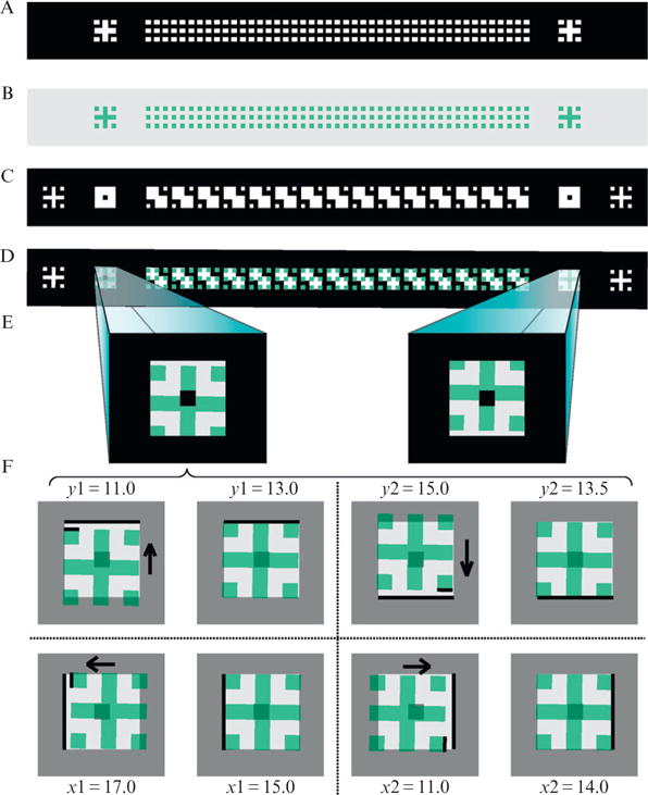
Sample layer alignment technique. (A) Photomask of layer #1, features are created by the transparent areas of the mask. (B) Features (green) on wafer (gray) for layer #1. (C) Photomask of layer #2. (D) Alignment of wafer with features from layer #1 to photomask for layer #2, as seen through the microscope of mask aligner. (E) Close-up view of alignment of the outermost left and right features. (F) For each side (left and right), the features on the wafer are aligned to the 4 four sides of the alignment box. The mask aligner micrometer position is averaged for x (15, 14) and y (13, 13.5) directions, to provide a single xy (14.5, 13.25) position. Note that it would seem that y1 and y2 positions should be identical if the feature sides are aligned to the alignment box. In reality, due to the new photoresist layer the features from previous layer become distorted, resulting in the difference. If the xy positions from the left and the right side are identical the alignment is good, otherwise the θ position needs to be changed and the whole process repeated. The transparency of the photomask has been adjusted for demonstration purposes.
Using the x, y, and θ micrometers on the mask aligner, find the alignment features from layer #1 and roughly position them under alignment elements of photomask for layer #2, Fig. 14.20D. Adjust the magnification of the mask aligner, so that most of your field of view is covered by a single alignment element, Fig. 14.20E.
Next, adjusting only the y-direction, align the top of the features to the top of the photomask alignment box. Record the position of y-direction micrometer, this is the y1 point. Repeat this step for the bottom side of the features and record the micrometer position, this is the y2 point. In a similar fashion obtain micrometer readings for alignment of left and right sides of the features to the alignment box, x1 and x2, Fig. 14.20F. Although it would seem that if the edges are aligned then position y1 would be equal to y2, and x1 equal to x2, however, this is rarely the case. In reality, the new photoresist layer makes the features seem somewhat distorted when viewed through the microscope. Though, assuming that the distortion is equal in all directions we can take the average of the two positions to get the actual aligned position, as seen by values in brackets in Table 14.11. Repeat the four measurements for the right side alignment element. Record all the data points into a table, as seen in Table 14.11.
Table 14.11.
Sample alignment datasheet
| θ | Left
|
Right
|
||
|---|---|---|---|---|
| X1, X2, | Y1, Y2, | X1, X2, | Y1, Y2, | |
| 17 | 15, 14, (14.5) | 13, 13.5 (13.25) | 16, 17 (16.5) | 11, 10 (10.5) |
| 15 | 14, 13, (13.5) | 14, 15 (14.5) | 17, 19 (18.0) | 9, 10 (9.5) |
| 19 | 15, 15 (15.0) | 12, 12.5 (12.25) | 16, 15 (15.5) | 14, 12 (13) |
| 20 | 15, 16 (15.5) | 12, 12 (12) | 16, 15 (15.5) | 12, 12 (12) |
In the first row of the table, the average positions for x and y are different for left and right sides. This would indicate that wafer is not aligned. Change the θ micrometer position by a small amount, in the example case we moved from 17 to 15. Repeating all the measurements it becomes evident that the left side and right sides are diverging from each other. This is probably not the right direction for θ movement. Move the θ from the initial position by the same amount in the opposite direction and repeat the measurements. In our example the θ position changed from 15 to 19. It is clear that the x–y positions are converging, but are not exactly equal yet. In the same direction, change θ position by the smallest possible step, and repeat measurements. If the positions are identical the wafer is aligned, if not, repeat θ movement and measurements. In our example, θ movement from 19 to 20 resulted in identical x–y positions for both sides, successfully terminating alignment procedure.
We have determined through experience that developing a systematic way of placing the wafer and the photomask into the mask aligner greatly reduces the time for alignment. The wafers we use have two flat edges, so when placing the wafer into mask aligner we find a surface on the mask aligner and roughly align the edge to that surface. The same trick is applied for the photomask. This results in relatively consistent placement of wafer and photomask, thus lowering the final alignment adjustments.
For the UV exposure step, set the x and y micrometer positions to the averaged values of x and y, respectively.
2.4. Soft lithography
Soft lithography is a microfabrication technique that relies on the use of a patterned elastomer to create structures, in our case, by cast molding. Although a number of different elastomers can be used, PDMS (polydimethysiloxane) has become the standard choice for microfluidics. PDMS is optically transparent, permeable to biologically important gases, chemically and thermally stable, the surface can be chemically modified and it does not absorb water. The PDMS we use comes as a two part kit: silicone monomer and curing agent. Mixing the components in specific ratio creates PDMS prepolymer that remains liquid for a few hours. The PDMS mold is prepared by pouring liquid prepolymer over a patterned wafer, curing it at elevated temperature and removing from the wafer. Since PDMS is initially in liquid phase, it easily conforms to the geometry of the wafer. Once cured, it remains flexible and allows for easy peel-off from the wafer. Furthermore, treating the wafer with a release agent improves the peel-off process (Duffy et al., 1998; Sia and Whitesides, 2003; Whitesides et al., 2001b; Xia and Whitesides, 1998). All the tools, chemicals and equipment required for soft lithography are listed in Table 14.12.
Table 14.12.
Soft lithography equipment, chemicals and supplies
| Equipment | Qty | Part No. | Vendor |
|---|---|---|---|
| Vacuum pump RV8 | 1 | A65401906 | Edwards |
| Vacuum pump EMF 10 exhaust mist filter | 1 | A46226000 | Edwards |
| Vacuum pump oil return kit | 1 | A50523000 | Edwards |
| Vacuum pump inlet connection (NW25 to 3/4″ hose barb) | 1 | NGT908000 | Edwards |
| Vacuum pump NW25 clamping ring | 1 | C10514401 | Edwards |
| Desiccators | 2 | 08-642-5 | Fisher Scientific |
| Ceramic desiccator plate | 2 | 08-642-10 | Fisher Scientific |
| Isotemp Oven | 1 | 506G | Fisher Scientific |
|
| |||
| Vacuum manifold parts | Qty | Part No. | Vendor |
|
| |||
| 1/2″ stainless steel hose clamps | 5 | 6151K51 | McMaster-Carr |
| 1″ stainless steel hose clamps | 5 | 6151K53 | McMaster-Carr |
| 1′ 3/4″ ID, 1″ OD wire-reinforced tubing | 5 | 5393K45 | McMaster-Carr |
| 1′ 1/4″ ID, 1/2″ OD wire-reinforced tubing | 10 | 5393K31 | McMaster-Carr |
| 3/4″ MPT to 3/4″ barb adapter | 1 | 5365K23 | McMaster-Carr |
| 3/4″ FPT to 3/4″ FPT to 1/4″ FPT tee | 1 | 4429K229 | McMaster-Carr |
| 1/4″ MPT to 1/4″ MPT nipple | 3 | 9171K122 | McMaster-Carr |
| 1/4″ FPT to 1/4″ to 1/8″ FPT tee | 3 | 4429K223 | McMaster-Carr |
| 1/4″ MPT to 1/4″ FPT-handle valve | 5 | 4912K87 | McMaster-Carr |
| −30 in Hg vacuum gauge with 1/8″ MPT at back | 3 | 3935K21 | McMaster-Carr |
| 3/4″ MPT to 1/2″ MPT reducing nipple | 1 | 9171K223 | McMaster-Carr |
| 1/2″ FPT to 1/2″ FPT to 1/2″ FPT tee | 1 | 4429K253 | McMaster-Carr |
| 1/2″ MPT to 1/4″ MPT reducing nipple | 2 | 9171K219 | McMaster-Carr |
| 1/4″ FPT to 1/4″ FPT to 1/4″ FPT tee | 2 | 4429K251 | McMaster-Carr |
| 1/4″ MPT to 1/4″ barb adapter | 2 | 53505K64 | McMaster-Carr |
| PTFE thread seal tap | 1 | 4591K12 | McMaster-Carr |
|
| |||
| Chemicals and supplies | Qty | Part No. | Manufacturer |
|
| |||
| Silicone elastomer kit | Sylgard 184 | Dow Corning | |
| (TRIDECAFLUORO-1,1,2,2-TETRAHYDROOCTYL)-1-TRICHLOROSILANE | T2492 | UCT | |
| Aluminium foil | |||
2.5. Soft lithography: Protocol
2.5.1. Aluminum holder
Cut out a 20-cm circle from aluminum foil. Place the wafer, features up, in the center of the foil. Next, carefully holding the wafer down, start to fold the foil up all the way around the perimeter. This will create 5 cm high walls around the wafer that will hold PDMS in. Make sure that the foil is really tight against the edge of the wafer, this prevents significant leaks of PDMS under the wafer.
2.5.2. Applying release agent (for new wafers only)
It is necessary to perform this step in a fume hood following all safety precautions, as most release agents are toxic. Place the wafer into a dedicated silanizing desiccator. Using a syringe with a needle, draw up the release agent, we use (TRIDECAFLUORO-1,1,2,2-TETRAHYDROOCTYL)-1-TRICHLOROSILANE. Deposit only a single drop (~ 30 μl) of the release agent into an open top small container inside the desiccator, see Fig. 14.21. Close the lid of the desiccator and turn on the vacuum. The release agent will vaporize and evenly deposit onto the wafer. Let this reaction happen for about 15 min. Using too much release agent will inhibit PDMS binding to glass coverslip.
Figure 14.21.
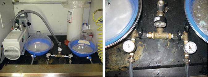
Vacuum pump and desiccators. (A) Vacuum pump and desiccators located in the fume hood. Each desiccators for a single purpose: (1) wafer silanizing (left) and (2) PDMS degassing (right). Note the opaqueness of the silanizing desiccator, this is due to silanizing agent vapor deposition over the years. (B) Vacuum manifold connecting the vacuum pump to the desiccators. The manifold allows for individual control of vacuum or atmospheric pressures to each desiccator. See Table 14.12 for parts list.
2.5.3. Preparing PDMS
In a clean weighing tray measure out, in a 10:1 ratio, and mix 40 grams of silicone elastomer base with 4 grams of silicon curing agent. Continue vigorously mixing with a clean spatula. The consistency of the mixture should start to change from clear to foamy. Mix the components thoroughly for 3 min.
2.5.4. Degassing PDMS
Mixing introduces a lot of air bubbles into the PDMS. To degas, place the weighing tray into the dedicated desiccator and turn on the vacuum. As pressure within the desiccator drops, the trapped air bubbles will expand and PDMS might spill out of the tray. Quickly releasing the vacuum should pop a significant portion of the bubbles. Turn on the vacuum again and repeat this cycle until there are no more bubbles. Depending on the vacuum pressure this should take 10–20 min. Also, it is possible to degas by pouring mixed PDMS into a 50-ml Falcon tube and centrifuging it at ~2700 g for 10 min.
2.5.5. Pouring PDMS
Place the wafer into the degassing desiccator and pour the PDMS over it. Since PDMS is very viscous, you might have to use a spatula to get all of it onto the wafer. This process will introduce new air bubbles into the PDMS. Repeat step 4 until there are no visible bubbles in the PDMS. Sometimes the PDMS will leak under the wafer and you will see bubbles forming around the perimeter of the wafer. You can ignore them when considering to stop degassing.
2.5.6. Curing
Place wafer in 80°C oven for 1 h.
2.6. PDMS processing
During the final phase of manufacturing the individual chips are cut out, cleaned and bonded to coverslips. Although the processing is performed in regular lab environment it is critical to get the chips and coverslips as clean as possible. This eliminates debris from the chip and improves the overall quality of the devices. To improve the final bond between PDMS and glass coverslip, it is recommended to complete soft lithography and PDMS processing in the same day. All the required materials and tools for this phase of manufacturing are listed in Table 14.13.
Table 14.13.
PDMS processing equipment, chemicals and supplies
| Equipment | Qty | Part No. | Vendor |
|---|---|---|---|
| Dissecting scope | 1 | ||
| Fiber optic light source | 1 | Dynalite 150 | A.G. Heinze, Inc. |
| UVO Cleaner | 1 | Model No. 42 | Jelight Company Inc. |
| Flowmeter | 1 | FR4A37 | Key Instruments |
| 1/8 Male pipe adapter Polyurethane tubing | 2 | 5454K65 | McMaster-Carr |
|
| |||
| Chemicals and supplies | Qty | Part No. | Manufacturer |
|
| |||
| Leur stub (25 gauge) | 75165A686 | McMaster-Carr | |
| Biopsy punch Harris Uni-Core 0.5 nm | 15071 | Tex Pella, Inc. | |
| Razor blades | 12-640 | Fisher Scientific | |
| 10 ml Disposable syringe | 14-823-2A | Fisher Scientific | |
| Cover slips No. 1 1/2, size: 24 × 40 mm, thickness: 0.16–0.19 mm | 12-530F | Fisher Scientific | |
| Magic Tape | 810 | Scotch | |
| Kimwipes, Kimberly-Clark No. 34155 | 06-666A | Fisher Scientific | |
| Compressed O2 | Medical grade | ||
| n-Heptane | HPLC grade | ||
| Methanol | HPLC grade | ||
| DI Water | Milli-Q or better | ||
2.7. PDMS processing: Protocol
2.7.1. Removing PDMS layer
Take the wafer out of the oven and let it cool down to room temperature. Carefully peel of the foil from PDMS. Some PDMS may have gotten under the wafer. You need to remove this layer prior to peeling off the top layer of PDMS. Using a razor blade, cut the bottom layer as close to the edge of the wafer as possible. It is also possible to rub the edge of the wafer with your gloved finger. This will break the PDMS on the edge, disconnecting the bottom and top layers of PDMS. Very slowly lift up the top layer of PDMS. Allow the PDMS to lift off from the wafer by itself, this is best done by raising a part of PDMS to a small height, stopping and letting the PDMS catch up. Lift up the PDMS in 3–4 places around the perimeter of the wafer, before peeling it off completely. Wafers are very brittle, so make sure not to twist or apply excessive pressure on it, as it will easily break. For safe storage place the wafer into a labeled wafer holder.
2.7.2. Cutting PDMS
Using the dissecting scope, examine the features on the PDMS. Sometimes the angle of the light source needs to be adjusted to get enough contrast to see the microscopic features. Placing the PDMS on a dark background also improves contrast. Next, using a razor blade carefully cut out individual chips, leaving extra room around the perimeter of the chip. Try to leave at least 3 mm of extra PDMS around each port, it will improve the chip’s bonding and prevent port leaks.
2.7.3. Punching ports
Place the chip with feature side up and, using the dissecting scope, locate the outline of the port. Place the tip of 25 gauge leur stub within the outline and, making sure it is as vertical as possible, apply downward pressure. The PDMS should first deform and then break; sometimes a final push is required to completely break through the PDMS on the exit. Next, carefully pick up the PDMS chip and remove the PDMS core using tweezers. Slowly pull out the puncher from the hole, while rotating it back and forth. Continue this for all ports on the chip. Sometimes the punching will tear the PDMS around the port, this is most likely due to a dull punching tip. Simply, swipe the punching tip against an abrasive surface 2–3 times and retry the punching. It is also possible to use a biopsy punch, which combines the leur stub and tweezers in a single tool, to make the holes.
2.7.4. Cleaning ports
Attach a 23-gauge leur stub to a syringe and fill it with DI water. Hold the tip of the leur stub against a port and apply pressure. A stream of water should exit from the other side of the chip. Keep the pressure for 3–5 s. Repeat this process of all ports on both sides of the chip.
2.7.5. Cleaning chips
Spray each chip with 70% Ethanol and gently rub using your gloved finger. Thoroughly rinse the chip with MilliQ quality water and blow dry using clean dry air. Make sure to dry both sides of the chip and all the ports. Place the dry chips in a clean Petri dish. Apply scotch tape to both sides of the chip. The next step is crucial for clean chips. Careful not to tear the PDMS, run your fingernail over the features a few times, covering the area of the whole chip. Repeat the scotch tape cleaning 3–5 times. Once done, use a fresh piece of tape to cover the chip and put the chip in the Petri dish.
2.7.6. Cleaning coverslips
Spray both sides of the coverslips with n-Heptane and gently rub the surface using your finger. To prevent the coverslip from breaking, apply pressure using your finger on both surfaces at the same time. Wipe the coverslip completely dry with a Kimwipe. Repeat the process using Methanol. Finally, wash the coverslips with DI water and dry using clean air. Make sure the coverslips are completely free of dust, spot or streaks. If you notice something, redo the DI water wash step. Once done, place the clean coverslips into a Petri dish and cover.
2.7.7. Bonding chips to coverslips
Open the compressed O2 valve on your tank and make sure the flow through the UVO cleaner is 0.4–0.6 scfm. Warm up the UVO cleaner, by running it for 5 min. Once the warm up is done, open the loading tray, there should be a faint smell of ozone. Place the chips with feature side up and coverslips onto the tray. Close the tray and run the bonder for 3 min. When done, open the tray and place the chip onto the coverslip using tweezers. To improve the bond, using tweezers, gently apply pressure around the perimeter of the chip. Make sure that chip and coverslip come in contact as soon as possible, as the chemistry allowing for bonding changes with time. Place bonded chips in 80°C oven overnight. If you have a lot of chips, it might be beneficial to break up the bonding step in 2 or more batches.
2.7.8. Troubleshooting
Poor chip bonding: this can be caused by a number of issues
Too much release agent used during wafer preparation. Try lowering the amount of release agent or shortening the coating time.
Check O2 supply to UVO bonder.
Expose the chips and coverslips exactly for 3 min. Make sure to bond chips and coverslips immediately after exposure to ozone.
Place a weight on top of the chips during overnight baking. Make sure not to break the coverslip.
Make sure all PDMS processing steps are done in one day.
Collapsed features
Usually only the lowest features will collapse, but if enough pressure is applied from the top of the chip even taller features are susceptible. Lower the amount of pressure applied on the top of the chip during bonding.
Try placing the coverslip on top of the chip during bonding. This should prevent features lower than 0.5 μm from collapsing.
3. Part III: Experiments
3.1. Experimental setup for E. coli
Although it is possible to perform microfluidic experiments without a lot of specialized equipment, we have found that purpose-built tools, such as our DAW and syringe towers, greatly increase productivity and experimental control. As mentioned in earlier sections, we use linear actuators to control the hydrostatic pressure of syringes, Fig. 14.23B. However, we use special syringe towers, as shown in Fig. 14.22, for controlling the height of our static syringes used for waste, cell and shunt ports. The towers are equipped with rulers, allowing us to record the position of syringes for an experiment. This data is used in subsequent experiments to reliably reproduce flows within the chip. Image data acquisition is performed by a Nikon fluorescence microscope, see Appendix for component list. Our complete experimental setup can be seen in Fig. 14.23A, and functional mDAW chip with attached lines in Fig. 14.23C.
Figure 14.23.
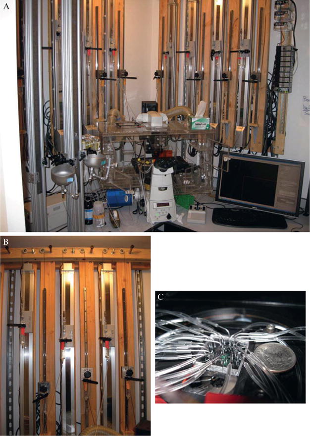
Experimental setup. (A) The equipment setup for mDAW experiments. In the background one can see the linear actuators, it is possible to fit all eight actuators and eight linear guides in a compact space behind the microscope. Fluorescent microscope with environmental chamber can be seen in the foreground of the image. (B) Three linear actuators with linear guides and pulley systems. This is a photograph of the system described in Fig. 14.15B. (C) An mDAW chip with all the connection pins and lines attached. U.S. dime coin (17.91 mm) is shown for scale.
Figure 14.22.
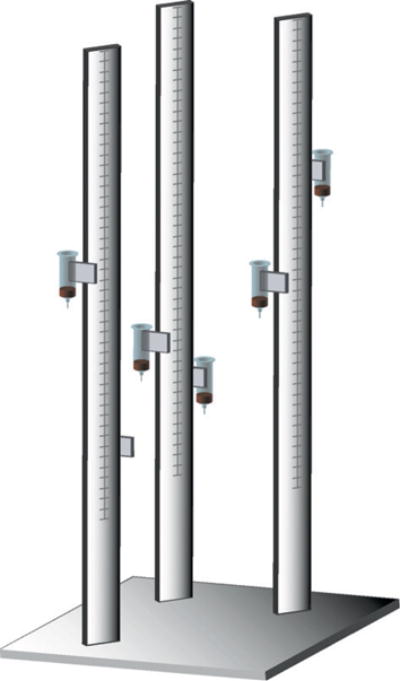
Syringe towers. Made from a commercially available erector set, the towers provide support for static syringes. We use a three pillar design with six adjustable platforms, which hold 2–9 syringes each. The ticked lines in the drawing represent rulers that are used for consistent syringe placement. All the parts necessary for constructing the tower are listed in Table 14.14.
For experiments, we modify our standard LB media, by adding 0.075% Tween 80 and filtering it through 0.22 μm filter. Addition of Tween 80 prevents the cells from sticking to chip walls without any noticeable harm to the cells. Depending on your experiment, make sure to add antibiotics and any inducers to the media.
3.1.1. Overnight culture
Grow up an overnight culture of cells from −80°C stock or from a plate. Grow the cells in 3 ml of LB media with appropriate antibiotics in 37°C shaker incubator.
3.1.2. Cell growth
Dilute the overnight culture by a factor of 1:1000 into 50 ml of fresh media with appropriate antibiotics and inducers. Let the cells grow up to a culture density of OD600 0.05–1.0, we usually try for OD600 0.1. Depending on the cell type this step should take 2–3 h. During this time perform steps 3–6.
3.1.3. Wetting the chip
Secure the chip in a chip holder, using rubber gaskets for additional contact. We have a custom chip holder, details for which can be provided by request. Basically, it securely holds a 24 × 40 mm cover slip, while allowing light access from the bottom, physical access from the top, and secure attachment to the microscope’s stage. Place the chip under microscope at 4× magnification. It is important to examine the chip for dirt and collapsed channels. This is best done at lower magnification, as you can see a larger area. Make sure that there is no debris blocking the channels or the imaging areas. Collapsed traps or channels will look darker and generally resemble in shade bonded parts of the chip. If the chip looks good proceed to wetting. Wetting the chip can be done using hydrostatic or manual pressure applied through a syringe. Attach a leur stub, a microfluidic line and a connection pin to a syringe and fill with fresh media. Make sure there are no bubbles in the syringe or the line. Bubbles can be removed by flicking the syringe or the line with your finger. Carefully insert the pin into a port. The color of the channels should start to change as fluid fills them. If using hydrostatic pressure to wet, position the syringe on the towers as high as possible and let the fluid flow through the chip. If using manual pressure, make sure to apply gentle pressure as too much pressure will lift the chip off the coverslip. As media fills the chip it will come up through the open ports and start forming droplets on the surface of the chip. Repeat this process for all the ports and until there are no more air bubbles in the chip. Media removal from the surface of the chip is best accomplished using a kimwipe.
3.1.4. Preparing syringes
Attach a sterile 23 gauge leur stub to a clean 60 ml syringe. Take 6 feet of Tygon tubing and gently slide it over the leur stub. Attach a connection pin to the other side of the tubing. A connection pin is basically just the metal part of a 23-gauge leur stub. We make them by pulling out the metals tips from the plastic part of the leur stub using pliers. The phase condensers on some microscope may come in contact with the straight connection pins. To circumvent this issue we make L-shaped pins by bending them around the shank of a 10–32 wood screw using pliers, refer to Fig. 14.24 for exact instructions on making straight and L-shaped pins.
Figure 14.24.
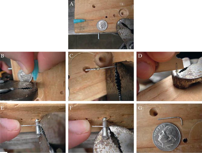
Making connection pins. (A) A nonsterile 23 gauge leur stub, dowel pin, and pliers are used to make the connection pins. (B) Using pliers grab onto the metal part of the luer stub, while holding the plastic part with your fingers. Pull them in opposite direction until they separate. (C) The metal pin alone, notice all the sealant and glue on it. (D) Using a razor blade, carefully remove all the glue from the outside of the pin. To make straight connection pins the process is finished at this point and pins just need to be cleaned in a sonicator. (E) Holding the pin with pliers, place it over the dowel pin. (F) While holding one of the ends of the pin with your finger, gently rotate the other end around the dowel pin. (G) Finished L-shaped connection pin. This method preserves the inner radius of the connection pin. Simple bending it will most likely pinch the pin. U.S. dime (17.91 mm) shown for scale.
Depending on the intended use for the syringe, remove the plunger and extract 100 μl of media or dH2O with a P200 pipetman. Insert the tip of the pipetman into the syringe and make contact with the inside of the leur stub adapter. Slowly expel the fluid into the leur stub adapter which should be enough to fill it, as shown in Fig. 14.25C–E. Adding fluid to the leur stub adapter in this way greatly reduces bubble formation. Tilt the syringe slightly and gently pour the rest of the media or dH2O into the top of the syringe, letting it run down the side before it reaches the base of the syringe. This also helps in preventing bubbles. Flick the leur stub connector to cause media to flow into the microbore tubing. If difficult bubbles are present, partially unscrew the leur stub adapter about one half turn and then retighten. This can help release bubbles. If fluid still will not enter the microbore tubing, use the syringe plunger to force the fluid in. Note if the plunger is necessary, it usually indicates a severe bubble problem. Make extra sure all bubbles are removed before proceeding. Watch the fluid flow carefully through the microbore tubing line to the exit point at the leur stub. Carefully look over the line to ensure no bubbles are present. If bubbles are present, flick the lines to release them and watch them flow to the end of the microbore tubing. Cover the syringe top using a piece of foil or parafilm, while leaving a small opening to the atmosphere. Label the syringes appropriately and make sure the connection tips do not touch any surface.
Figure 14.25.
Experimental line and syringe techniques. (A) General guide for flicking a microfluidic line. Hold the line between the thumb and index finger of one hand, while flicking the downstream the line with a finger on your other hand. In the figure, the hands are place on the line so that the left hand is closer to the syringe and the right hand is closer to the microfluidic chip. (B) Technique for gentle agitation of fluid within the microfluidic device. Hold the line between thumb and index finger. Gently move the line back and forth using your ring finger. The ring finger is placed on the line toward the microfluidic device. (C) Wetting of the MDAW chip using a specially designed manifold. (D) Technique for minimizing bubbles during syringe preparation. Using a P200 pipetman draw up 100 μl of desired liquid. Remove the plunger from the syringe. Insert the pipetman into the syringe and hold both at a slight angle. (E) Insert the pipette tip all the way into the leur stub adapter and slowly expel the liquid. (F) Flicking the bottom of the syringe to fill the connection pin with liquid.
3.1.5. Connecting syringes
Attach all the syringes to the sliders on the microfluidic tower, as seen in Fig. 14.22. Adjust syringe heights appropriately. To prevent contamination of the media source, make sure it is always the highest positioned syringe. One by one, starting with the media, connect each syringe to the chip. Since the cells are not ready yet, connect a syringe filled with DI water to the cell port. Examine that no bubbles were introduced into the chip during this process. If there are bubbles, see if they can slowly disappear on their own. However, it might be necessary flush the chip by disconnecting all the syringes and repeating step 3. Once all the bubbles have been eliminated, using scotch tape secure each line to the chip holder. Tape far enough away from the chip, so that the bending of the tubing is not applying a force on the connection pin.
3.1.6. Setting up DAW software
Using the software, calibrate the syringe heights for correct mixing ratios. Create a desired profile for the syringe movement. Make sure that all the static syringes are in their “running” positions.
3.1.7. Spinning down cells
When the cells are ready, spin them down at 2700 g for 10 min. As a backup, pour the supernatant media back into the flask and place it in incubator. Add 2–3 ml of fresh media to the pelleted cells and gently vortex them, until there are no cell clumps. Load the cells into a prepared syringe. Once again, make sure there are no bubbles.
3.1.8. Loading cells
Move all syringe to their “loading” positions. Disconnect the temporary cell syringe and plug in the actual cell syringe. At this point the flow from the media and the cell port both should be going toward the waste port. At 20× magnification you should be able to see cells flowing through the channels. Adjust the height of the cell syringe so that the cells are slowly moving past the traps. Next, securely hold the cell line between the thumb and index finger of one hand, while flicking the line with a finger on your other hand as seen in Fig. 14.25A. Imagine that the pinching fingers divide the line into two parts: the syringe part and the connection pin part. The flicking should be done on the connection pin part of the line. The cells should rapidly move back and forth within the chip, as the flicking wave propagates down the line. Adjust the flicking strength to have enough force to load the traps. Once enough traps have been loaded, adjust the syringe heights to their “running” positions. Media flow should be 20–200 μm/s.
3.1.9. Starting experiment
Allow the cells to grow in the traps for 3–5 doublings, depending on your cell type this should take 1–2 h. Setup the microscope software for automated image acquisition, this includes auto-focus, various position on the chip and required light channels, i.e. phase-contrast, fluorescence. Start the imaging and the iDAW software at the same time.
3.1.10. Checking on cells
During the experiment it might be necessary to remove stuck cells from the channels. Hold the cell line between the thumb and index finger with your middle finger further away from the syringe. Gently move the line back and forth using your ring finger and watch as the cells smoothly mirror the motion, see Fig. 14.25B for a visual representation. This technique is useful for getting rid of stuck cells or controllably reducing cell density within a trap.
3.2. Method to set up a MDAW microfluidic experiment
In this section we will describe how to set up a microfluidics experiment using the MDAW parallel DAW microchemostat chip since this chip presents challenges not seen for smaller chips.
3.2.1. Pre-experiment preparation
See Table 14.14 for the catalog numbers of supplies listed here. The steps described in this section should be performed at least 1 day in advance of the experiment. The microfluidic devices themselves should be prepared as described in Section 2.6. Cut 26 lines using Tygon microbore tubing seven feet in length. Note the line length is dependent on the microscopy setup, there should be some slack to allow for movements of the syringe reservoirs. Obtain 26 sterile 30 ml syringes. Note for the combined ports we use 4 inch stainless steel pipe caps fitted with leur stub adapters. If these pipe caps are used, then only twenty-four 30-ml syringes are necessary. These pipe caps were manufactured by our university’s machine shop, details can be provided by request. Due to their large diameter, the liquid height in the pipe caps changes very little for a given volume of accumulated fluid. This is important since the combined ports receive vastly more fluid then the individual ports during an experiment. If a 30-ml syringe were used instead of a pipe cap, it is conceivable that the height increase would affect flows in the chip over the course of a long experiment (2–3 days). See Fig. 14.5 and the accompanying text for an example of these issues.
Table 14.14.
Experimental equipment, Chemicals and supplies
| Equipment | Qty | Part No. | Vendor |
|---|---|---|---|
| Inverted fully automated microscope | 1 | Ti | Nikon |
| PDMS chip holder | 1 | Custom | |
| Syringe towers | |||
| Aluminum bread board, 12″ × 12″, 1/4-20 threaded | 1 | MB12 | Thorlabs, Inc. |
| 1″ × 3″ Extrusion 60″ long | 3 | 1030 × 60″ | 80/20, Inc. |
| 8 Hole inside corner gusset | 3 | 25-4138 | 80/20, Inc. |
| Slide-in T-nut | 6 | 3382 | 80/20, Inc. |
| Double Slide-in T-nut | 6 | 3280 | 80/20, Inc. |
| 1/4-20 × 1/2″ Flanged button head socket cap screw | 6 | 3342 | 80/20, Inc. |
| 1/4-20 × 1/2″ Socket head cap screw | 12 | 3062 | 80/20, Inc. |
| 1/4-20 × 3/8″ Socket head cap screw | 6 | 3058 | 80/20, Inc. |
| 1/4″ washer—black zinc | 20 | 3258 | 80/20, Inc. |
| Double flange linear bearing brake kit ready | 8 | 6425 | 80/20, Inc. |
| Ratcheting L-handle | 8 | 6850 | 80/20, Inc. |
| White UHMW Pads w/brake hole | 24 | 6490 | 80/20, Inc. |
| #8 × 3/8″ SS standard bearing pad screw | 24 | 3625 | 80/20, Inc. |
| 48″ stainless steel rule | 3 | 2120A15 | McMaster-Carr |
| 1″ adjustable strap | 1 Pkg | 7565K51 | McMaster-Carr |
| Chip holder rubber gasket | 7665K11 | McMaster-Carr | |
|
| |||
| Chemicals and supplies | Qty | Part No. | Manufacturer |
|
| |||
| Connection pins (23 gauge, ID 0.017′, OD 0.025″, 1/2″ Long) | 75165A684 | McMaster-Carr | |
| Single use, sterile leur stub (23 gauge) | 14-826-19E | Fisher Scientific | |
| Reusable leur stub (23 gauge, ID 0.017″, OD 0.025″, 1/2″ Long) | JGM23-0.5D | Jensen Global Inc | |
| Disposable syring 10 ml w/leur lock tip | 14-823-2A | Fisher Scientific | |
| Disposable syring 30 ml w/leur lock tip | 14-829-48A | Fisher Scientific | |
| Disposable syring 60 ml w/leur lock tip | 13-689-8 | Fisher Scientific | |
| Tygon flexible microbore tubing (ID 0.020″, OD 0.060″) | 1 | 14-170-15B | Fisher Scientific |
| Tween 80 | 1 | P8074 | Sigma-Aldrich |
| Alconox 1104 | 1 | 04-322-4 | Fisher Scientific |
| Liquid cell media | |||
| DI Water | Milli-Q or better | ||
To clean the metal parts, sonicate twenty-six reusable leur stub adapters, twenty-six 90° curved connection pins (see Figure 14.24), and the pipe caps if they are to be used, for 60 min at 60°C in a 250-ml beaker containing 1% w/v Alconox. Sonication in 1% w/v Alconox does an excellent job of removing cell debris and residual media from small metal parts. After sonication rinse the parts in dH2O. Flush water through the leur stub adapters and connection pins to remove residual Alconox. We use a manifold to flush all metal parts at once, see Fig. 14.25C. In general, we flush 3 l of dH2O through the entire system for rinsing. After flushing with water, air can be flushed for drying. Autoclave the leur stubs, adapters and, if using them, pipe caps for 30 min on a dry cycle.
Prepare the 26 (24 if using pipe caps) syringe reservoirs as described in Section 3.1.4. Cut 8 sections of red, orange and yellow tape. Write 1–8 on each of the colored tape sets and affix to the syringe bodies. The tape will help to identify the syringe reservoirs later in the setup. Each of the eight subexperiments has two DAW input ports (A and B) and a cell port (C). We use the red tape to refer to A reservoirs, orange for B and yellow for C. Cut another three sets of colored tape and again write 1–8 on each set. Affix the tape near the end of the microbore tubing (just before the connection pin) for the appropriate reservoir. Labeling the end of the tubing helps to identify its connected reservoir, a necessity when many lines are nested together. Use scotch tape to affix the loose microbore tubing end to the syringe.
3.2.2. Cell Growth
Determine how many cell cultures will be needed, a maximum of eight can be used. Inoculate the cell cultures the day before the experiment with the appropriate media and additives. In the next morning check the culture optical density at 600 nm (OD600) using a spectrophotometer. Grow cells at 30°C for ~4 h, to an OD600 of ~1.0 upon cell loading.
3.2.3. Media preparation
Prepare 4 ml of media for each of the 16 input syringes (ports A and B for each of the eight subexperiments). Generally the media is the same in the two inputs except for the tested component. See Table 14.15 for an example of the media composition. Add dye to one of the two input reservoirs for each subexperiment to use as an inducer tracer. After the media has been prepared, add it to each of the A and B syringe reservoirs as described in Section 3.1.4. Add sterile dH2O to the shunt and alternate waste reservoirs. If 30 ml syringes are used, add 4 ml of dH2O. If pipe caps are used add ~100 ml.
Table 14.15.
Experimental equipment, chemicals and supplies
| Ingredients | Stock | Final | Units | Lot | 1X (μL) | 2.5X (mL) | |
|---|---|---|---|---|---|---|---|
| 1 | 2X SC—met media | 2 | 1 | X | 2000 | 5 | |
| 2 | Methionine | 50,000 | 500 | μM | 40 | 0.1 | |
| 3 | Galactose | 2 | 0.2 | %w/v | 400 | 1 | |
| 4 | Raffinose | 20 | 2 | %w/v | 400 | 1 | |
| 5 | ddH20 | – | – | – | 1160 | 2.9 | |
| total: | 4000 | 10 |
3.2.4. Air removal from the chip
Note that this procedure differs from that of a smaller chip (such as MFD005a). While removal of air can also be facilitated using a vacuum, we have found this to interfere with our cell’s growth under some conditions. Affix a bonded MDAW chip onto a solid substrate, like a glass plate or a microscopy chip holder, as the one described in Step 3 of E. coli experimental section. Fill a 10-ml syringe with a sterile solution of 0.1% v/v Tween 80 and connect it to the central port of the chip (called the alternate waste port). Tween 80 is a surfactant that aids in clearing bubbles. It also acts as a lubricant that prevents cell clogging. Purge air from the chip by applying force to the syringe. Watch for droplets to appear at each port indicating that fluid has propagated through the chip’s channel network.
We have a custom built 26 outlet manifold connected to a pressure reservoir filled with dH2O. Each outlet of the manifold is connected to a half meter of teflon microbore tubing with a connection pin at the end. The manifold is fully autoclavable and by pressurizing all ports at once, achieves better clearance of air. Details of the manifold’s construction can be provided upon request. To purge air from the manifold we pressurize it until water flows out of each connection pin. Next we connect each pin to a port on the chip, making sure a “fluidic connection” is made, that is, there is a visible droplet of fluid above each port on the chip and fluid is leaving the connection pin of the manifold. When the manifold is fully connected it is then pressurized to 4 Psi for 5 min to flush all air from the system.
3.2.5. Connecting DAW reservoirs to the device
After the air has been purged from the system, place the chip in a microscopy holder if not done already. Secure both ends of the device with scotch tape. Place the chip above the microscope stage. Our microscope has an acrylic environmental chamber around it, whose top is about 25 cm above the stage height. We place the chip on top of this box. Attach the shunt and alternate waste port reservoirs to the syringe towers. Adjust the height of the shunt reservoir to 30 cm above the stage. Adjust the height of the alternate waste reservoir to 37.5 cm above the stage. Take the connection pin from the shunt reservoir and place it several centimeters below the reservoir’s fluid level. Wait for fluid to exit the end of the microbore tubing line and then connect the leur stub to the shunt port at the top of the device. Repeat this procedure to connect the alternate waste reservoir to the device. Connect the DAW input reservoirs for each subexperiment to each set of A and B ports on the device using the same procedure. After connecting the reservoirs attach them to the linear actuators. The linear actuators should be set so each reservoir is 60 cm above the stage height. Once all of the input reservoirs have been connected, bundle the lines together with scotch tape so they do not become unwieldy.
3.2.6. Processing and loading cells
At this time remove the cell cultures from the incubator and record the final OD600 value if desired. Add Tween 80 to each cell culture to a final concentration of 0.1% v/v. Vortex on a medium setting to mix. Add each culture to the appropriate syringe reservoir as described in Section 3.1.4. Be extra careful there are no bubbles in any of the cell reservoirs. While using Tween 80 helps to prevent bubbles, any that remain in the reservoir will make it extremely difficult to load cells later on. The Tween 80 will also prevent clogging of the device by excess cells.
Adjust the height of the shunt port to 11.25 cm above the height of the stage and make sure the cell reservoir holder is set to 32.5 cm above stage height. This adjustment will ensure cells flow into the shunt and not other cell ports. At this time, all cell ports will contain a bead of fluid above them since they are the outlets for the other connected reservoirs. This bead of fluid will essentially function as a small reservoir. Since the device should still be placed at 25 cm above stage height, this will be the pressure of each cell port before its reservoir is connected. Once the shunt port is lowered there will be a net flow between the fluid bead of each cell port and the shunt. When the cell reservoirs are connected their pressure will increase to 32.5 cm. If the shunt port were not lowered some flow would exit at the unconnected cell ports, possibly causing cross-contamination.
Once all cell ports have been connected, place the chip into the microscope and tape down all microbore tubing lines. Adjust the height of the cell ports to 40 cm and observe the cells entering the system at 4× magnification. If cells are not entering from the cell ports it is usually due to residual bubbles in the cell lines. Disconnect if necessary and make sure there are no bubbles. Adjust the height of the alternate waste port to force more cells into the central region of the trap if necessary. Flick the lines for each cell port to load cells into the trapping region. Continue this procedure until an adequate number of cells have been loaded (generally 20–40 yeast cells). Once the cells have been loaded adjust the heights of all reservoirs as follows: Cell ports: 15.5 cm, combined alternate waste: 14 cm, combined shunt: 11.25 cm. All heights above stage height. The level of the DAW inputs should remain at 60 cm above stage height. If desired move to the DAW junction of each subexperiment and record the height positions for 0% and 100% mixing ratios or use the calibration procedure described in Section 1.1.5.
3.2.7. Microscope setup
Record the stage locations for each of the cell traps in the eight subexperiments in the microscopy software. Switch to a 40× or 60× objective and add microscopy oil as necessary. Update the xy positions for each trap as they will have changed slightly. Set up the microscopy software for a multiple location experiment, using appropriate exposure settings for phase contrast and any fluorescence wavelengths. Make sure the autofocus routine is properly set up. Since the MDAWchip is quite large, there will likely be a z-offset between the cell traps of each subexperiment. This z offset needs to be compensated for. Moreover, due to stage drift over the course of an experiment the z offset will shift in time. Some microscope software packages cannot cope with this properly and we have written a custom macro for the NI Elements software to compensate for this changing z offset. The macro uses the median of the last five focal planes for each cell trap to calculate an updated z offset. This z offset is used as the best guess for where to start the next iteration’s autofocus routine. Taking the median prevents a single poor autofocus result from causing a catastrophic loss of focus, which can happen if a bubble in oil droplet drifts into the field of view. We have had good success with this macro, retaining focus even after almost 72 h of an experiment. Set the linear actuator controller software for the proper input waves as described in Section 1.4.2. Begin image acquisition.
Acknowledgments
This project was supported by Grant Number P50GM085764 from the National Institutes of Health.
Appendix: Components of Nikon Ti Nikon Ti automated fluorescence microscope
| Description | Qty | Part No. |
|---|---|---|
| Ti-E Inverted Microscope | 1 | MEA53100 |
| Ti-HUBC/A Hub Controller A | 1 | MEF55030 |
| Ti-HC/A AC Adapter for HUBC/A | 1 | MEF51010 |
| Ti-AC120 Power Cord 120 V | 1 | MEF51200 |
| USB 2.0 Cable A-B 15′, Required for DS-U2 Controller | 1 | 97050 |
| Ti-DH Dia Pillar Illuminator 100 W | 1 | MEE59905 |
| D-LH/LC Precentered Lamphouse with LC | 1 | MBE75221 |
| Halogen Lamp 12 V 100 W L.L. | 3 | 84125 |
| Ti-PS100 W Power Supply 100–240 V | 1 | MEF52250 |
| Ti-100WRC 100 W Lamphouse Remote Cable | 1 | MEF51001 |
| Power Cord | 3 | 79035 |
| Filter 45 mm GIF | 1 | MBN11200 |
| Filter 45 mm NCB11 | 1 | MBN11710 |
| 45 mm Heat Absorbing Filter | 1 | MBN11500 |
| Eclipse Microscope Pad | 1 | 92080 |
| Eclipse Large Nylon Cover 14 × 26 × 32 | 1 | 92084 |
| Package Lens Tissue 50 Sheets, 4 × 6 | 1 | 76997 |
| CFI 10× Eyepiece F.N. 22 mm | 2 | MAK10100 |
| Ti-TD Eyepiece Tube D | 1 | MEB52320 |
| Ti-T-B Eyepiece Tube D | 1 | MEB55800 |
| Ti-S-ER Motorized Stage With Encoders | 1 | MEC56100 |
| Ti-SH Universal Holder for Motor Stage | 1 | MEC59110 |
| Ti-S-C Motorized Stage Controller | 1 | MEF55710 |
| Ti-S-EYOU Joystick for Motorized Stage | 1 | MEF55700 |
| Ti-CT-E Motorized Condenser Turret | 1 | MEL51910 |
| Ti-C-LWD LWD Lens Unit for System Condenser Turret | 1 | MEL56200 |
| System LWD Ph L Annuli | 1 | MEH31040 |
| TE-C LWD Ph1 Module | 1 | MEH41100 |
| TE-C LWD Ph2 Module | 1 | MEH41200 |
| TE-C LWD Ph3 Module | 1 | MEH41300 |
| Ti-ND6-E Sextuple Motor Dic Nosepiece | 1 | MEP59310 |
| CFI Plan Fluor DL 4 × NA 0.13 WD 17.1 mm | 1 | MRH20041 |
| CFI Plan Fluor DL 10 × NA 0.3 WD 16.0 mm | 1 | MRH20101 |
| CFI Plan Fluor DLL 20 × NA 0.5 WD2.1 mm Sprg | 1 | MRH10201 |
| CFI Plan FLUOR DLL40 × OIL NA 1.3/WD 0.2MM | 1 | MRY10018 |
| CFI Plan APO DM 60 × Oil | 1 | MRD31602 |
| CFI Plan APO DM 100 × Oil | 1 | MRD31901 |
| 50 cc Immersion Oil Each | 2 | MXA20234 |
| C-FL GFP HC HISN Zero Shift | 1 | 96362 |
| C-FL TRITC HYQ | 1 | 96321 |
| C-FL YFP HC HISN Zero Shift | 1 | 96363 |
| C-FL CFP HC HISN Zero Shift | 1 | 96361 |
| C-FL Texas Red HC HISN Zero Shift | 1 | 96365 |
| Ti-FL Epi-Fl Iilluminator for Ti-Series | 1 | MEE54100 |
| Ti-FLC-E Motorized Epi-Fl Filter Turret for Ti-Series | 1 | MEV51110 |
| Lumen 200 Illumination System | 1 | 77011315 |
| SmartShutter controller | 1 | 77016099 |
| 35 mm SmartShutter w/stand-alone housing | 2 | 77016096 |
| Excitation Adapter for SmartShutter | 1 | 77016169 |
| Transmitted Light Adapter for Ti, 35 mm | 1 | 77016168 |
| Ti Shutter Trigger Cable for Sutter | 2 | MXA22088 |
| Ti Emission Adapter | 1 | 77016182 |
| NIS-Elements software | 1 | MQS31000 |
| NIS-Elements: Module 6D imaging | 1 | MQS42560 |
| NIS-Elements: Hardware Module | 1 | MQS41220 |
| C-Mount/ISO Adapter, 1 × | 1 | MQD42000 |
| CoolSNAP HQ2 Monochrome Camera | 1 | 77018219 |
| Nikon Environment-Chamber | 1 | 77065000 |
References
- Bao JB, Harrison DJ. Measurement of flow in microfluidic networks with micrometer-sized flow restrictors. AlChE J. 2006;52(1):75–85. [Google Scholar]
- Beebe DJ, Mensing GA, Walker GM. Physics and applications of microfluidics in biology. Annu Rev Biomed Eng. 2002;4:261–286. doi: 10.1146/annurev.bioeng.4.112601.125916. [DOI] [PubMed] [Google Scholar]
- Bennett MR, Pang WL, Ostroff NA, Baumgartner BL, Nayak S, Tsimring LS, Hasty J. Metabolic gene regulation in a dynamically changing environment. Nature. 2008;454(7208):1119–1122. doi: 10.1038/nature07211. [DOI] [PMC free article] [PubMed] [Google Scholar]
- Brody JP, Yager P, Goldstein RE, Austin RH. Biotechnology at low reynolds numbers. Biophys J. 1996;71(6):3430–3441. doi: 10.1016/S0006-3495(96)79538-3. [DOI] [PMC free article] [PubMed] [Google Scholar]
- Cookson S, Ostroff N, Pang WL, Volfson D, Hasty J. Monitoring dynamics of single-cell gene expression over multiple cell cycles. Mol Syst Biol. 2005;1:0024. doi: 10.1038/msb4100032. 2005. [DOI] [PMC free article] [PubMed] [Google Scholar]
- Danino T, Mondragn-Palomino O, Tsimring L, Hasty J. A synchronized quorum of genetic clocks. Nature. 2010;463(7279):326–330. doi: 10.1038/nature08753. [DOI] [PMC free article] [PubMed] [Google Scholar]
- del Campo A, Greiner C. Su-8: A photoresist for high-aspect-ratio and 3d submicron lithography. J Micromech Microeng. 2007;17(6):R81–R95. [Google Scholar]
- Dertinger T, Pacheco V, von der Hocht I, Hartmann R, Gregor I, Enderlein J. Two-focus fluorescence correlation spectroscopy: A new tool for accurate and absolute diffusion measurements. Chemphyschem. 2007;8(3):433–443. doi: 10.1002/cphc.200600638. [DOI] [PubMed] [Google Scholar]
- Duffy DC, McDonald JC, Schueller OJA, Whitesides GM. Rapid prototyping of microfluidic systems in poly(dimethylsiloxane) Anal Chem. 1998;70:4974–4984. doi: 10.1021/ac980656z. [DOI] [PubMed] [Google Scholar]
- Hersen P, McClean MN, Mahadevan L, Ramanathan S. Signal processing by the hog map kinase pathway. Proc Natl Acad Sci USA. 2008;105(20):7165–7170. doi: 10.1073/pnas.0710770105. [DOI] [PMC free article] [PubMed] [Google Scholar]
- Hong JW, Studer V, Hang G, Anderson WF, Quake SR. A nanoliter-scale nucleic acid processor with parallel architecture. Nat Biotechnol. 2004;22(4):435–439. doi: 10.1038/nbt951. [DOI] [PubMed] [Google Scholar]
- Kurth F, Schumann CA, Blank LM, Schmid A, Manz A, Dittrich PS. Bilayer microfluidic chip for diffusion-controlled activation of yeast species. J Chromatogr A. 2008;1206(1):77–82. doi: 10.1016/j.chroma.2008.07.058. [DOI] [PubMed] [Google Scholar]
- Lee PJ, Helman NC, Lim WA, Hung PJ. A microfluidic system for dynamic yeast cell imaging. Biotechniques. 2008;44(1):91–95. doi: 10.2144/000112673. [DOI] [PubMed] [Google Scholar]
- Lide D. CRC handbook of chemistry and physics: a ready-reference book of chemical and physical data. CRC Pr I Llc 2004 [Google Scholar]
- Mather W, Mondragon-Palomino O, Danino T, Hasty J, Tsimring LS. Streaming instability in growing cell populations. Phys Rev Lett. 2010;104(20):208101-1–208101-4. doi: 10.1103/PhysRevLett.104.208101. [DOI] [PMC free article] [PubMed] [Google Scholar]
- MicroChem. Microchem corporation. su-8 photoresist product line. 2010 http://www.microchem.com/products/su_eight.htm.
- Miura K. Tracking movement in cell biology. Adv Biochem Eng Biotechnol. 2005;95:267–295. doi: 10.1007/b102218. [DOI] [PubMed] [Google Scholar]
- Mosig A, Jager S, Wang C, Nath S, Ersoy I, Palaniappan K, Chen S. Tracking cells in life cell imaging videos using topological alignments. Algorithms Mol Biol. 2009;4(1):10. doi: 10.1186/1748-7188-4-10. [DOI] [PMC free article] [PubMed] [Google Scholar]
- Nguyen N, Wereley S. Fundamentals and Applications of Microfluidics. Artech House Publishers; 2002. [Google Scholar]
- Owens J, Houston M, Luebke D, Green S, Stone J, Phillips J. Gpu computing. Proc IEEE. 2008;96(5):879–899. [Google Scholar]
- Rowat AC, Bird JC, Agresti JJ, Rando OJ, Weitz DA. Tracking lineages of single cells in lines using a microfluidic device. Proc Natl Acad Sci USA. 2009;106(43):18149–18154. doi: 10.1073/pnas.0903163106. [DOI] [PMC free article] [PubMed] [Google Scholar]
- Sia SK, Whitesides GM. Microfluidic devices fabricated in poly(dimethylsiloxane) for biological studies. Electrophoresis. 2003;24(21):3563–3576. doi: 10.1002/elps.200305584. [DOI] [PubMed] [Google Scholar]
- Stroock AD, Dertinger SK, Ajdari A, Mezic I, Stone HA, Whitesides GM. Chaotic mixer for microchannels. Science. 2002;295(5555):647–651. doi: 10.1126/science.1066238. [DOI] [PubMed] [Google Scholar]
- Sveen J. An introduction to matpiv v 1.6.1. Department of Mathematics, University of Oslo; Oslo, Norway: 2004. (Eprint series). 2004. Author Affiliations Bruno Moulia Biomechanics Group, Institut National de la Recherche Agronomique 234. [Google Scholar]
- Taylor RJ, Falconnet D, Niemisto A, Ramsey SA, Prinz S, Shmulevich I, Galitski T, Hansen CL. Dynamic analysis of mapk signaling using a high-throughput microfluidic single-cell imaging platform. Proc Natl Acad Sci USA. 2009;106(10):3758–3763. doi: 10.1073/pnas.0813416106. [DOI] [PMC free article] [PubMed] [Google Scholar]
- Thorsen T, Maerkl SJ, Quake SR. Microfluidic large-scale integration. Science. 2002;298(5593):580–584. doi: 10.1126/science.1076996. [DOI] [PubMed] [Google Scholar]
- Whitesides GM, Ostuni E, Takayama S, Jiang X, Ingber DE. Soft lithography in biology and biochemistry. Annu Rev Biomed Eng. 2001a;3:335–373. doi: 10.1146/annurev.bioeng.3.1.335. [DOI] [PubMed] [Google Scholar]
- Whitesides GM, Otuni E, Takayama S, Jiang X, Ingber DE. Soft lithography in biology and biochemistry. Annu Rev Biomed Eng. 2001b;3:335–373. doi: 10.1146/annurev.bioeng.3.1.335. [DOI] [PubMed] [Google Scholar]
- Williams MS, Longmuir KJ, Yager P. A practical guide to the staggered herringbone mixer. Lab Chip. 2008;8(7):1121–1129. doi: 10.1039/b802562b. [DOI] [PMC free article] [PubMed] [Google Scholar]
- Xia Y, Whitesides GM. Soft lithography. Annu Rev Mater Sci. 1998;28:153–184. [Google Scholar]
- Young ME, Carroad PA, Bell RL. Estimation of diffusion-coefficients of proteins. Biotechnology and Bioengineering. 1980;22(5):947–955. [Google Scholar]