Significance
The nitrogen vacancy center (NV) in diamond is a fluorescent color center that can be in several charge states depending on its local electrostatic environment. Here, we demonstrate the control of the charge state and fluorescence of NVs in nanodiamonds (NDs) by applying a potential difference across NDs in an electrochemical cell. Controlling the charge state can improve spin-based sensing protocols of the NV. Conversely, the NV’s strong fluorescence dependence on electrochemical potential differences also enables a new modality for optical sensing of its environment. With this electrochemical setup, we show that a single NV can reveal a 100-mV potential swing, whereas multiple NVs allow for the detection of potential swings as small as 20 mV.
Keywords: nitrogen vacancy center, nanodiamond, fluorescence microscopy, voltage sensing, voltage indicator
Abstract
The negatively charged nitrogen vacancy (NV−) center in diamond has attracted strong interest for a wide range of sensing and quantum information processing applications. To this end, recent work has focused on controlling the NV charge state, whose stability strongly depends on its electrostatic environment. Here, we demonstrate that the charge state and fluorescence dynamics of single NV centers in nanodiamonds with different surface terminations can be controlled by an externally applied potential difference in an electrochemical cell. The voltage dependence of the NV charge state can be used to stabilize the NV− state for spin-based sensing protocols and provides a method of charge state-dependent fluorescence sensing of electrochemical potentials. We detect clear NV fluorescence modulation for voltage changes down to 100 mV, with a single NV and down to 20 mV with multiple NV centers in a wide-field imaging mode. These results suggest that NV centers in nanodiamonds could enable parallel optical detection of biologically relevant electrochemical potentials.
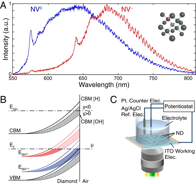
The nitrogen vacancy (NV) center is a fluorescent point defect in diamond formed by a substitutional nitrogen atom adjacent to a carbon vacancy (Fig. 1A). The negative charge state (NV−) is optically addressable and has a long-lived electronic spin state suitable for quantum sensing of local electric and magnetic fields (1–4). However, under constant laser illumination, the NV center can stochastically switch between the negatively charged state and the neutral charge state, NV0 (5, 6). Because the NV0 state lacks the NV− state’s favorable spin properties, there has been efforts to engineer stable NV− centers in diamond devices (7). Studies have shown that the diamond surface termination strongly affects the charge state of NVs near the surface: hydrogen surface termination increases the fraction of NV0 over NV−, whereas oxygen surface termination has the opposite effect (8). This dependence is due to the differences in band bending that the two types of surface terminations induce in diamond under ambient conditions. As illustrated schematically in Fig. 1B, NV centers that are deep below the surface can be in the negative charge state as the ENV0/− charge state transition level is below the Fermi level, EF. Hydrogen terminated diamond surfaces have a negative electron affinity (χ), which induces band bending near the surface as the Fermi level equilibrates with surface adsorbate states (μ) present in atmospheric conditions. Near the surface, this upward band bending shifts the ENV0/− level above EF, converting the near-surface NV centers to NV0. Band bending does not occur to the same degree for strongly oxidized diamond surfaces as they exhibit a large positive electron affinity and near surface NV centers remain in the negative charge state (8). However, some oxygen surface termination moieties such as hydroxyl groups can result in either positive or negative electron affinities depending on the type of surface reconstruction and crystallographic orientation of the diamond surface, which can also induce upward band bending in the diamond and affect the NV charge state (Fig. 1B) (9–11). In addition to the neutral and negative charge states, the NV center has been observed in a nonfluorescent state attributed to the positively charged state NV+ (12–16). The large band bending at hydrogenated surfaces can shift the corresponding ENV+/0 transition level and convert NVs closest to the surface from the NV0 state to the nonfluorescent NV+ state (Fig. 1B).
Fig. 1.
NV fluorescence and experimental setup schematic. (A) Fluorescence emission spectra of neutrally (blue) and negatively (red) charged NV centers in HPHT NDs. (Inset) Illustration of the NV center in the diamond lattice. (B) Energy band structure schematic showing the band bending near hydrogen (solid) and hydroxyl (dashed) terminated diamond surfaces in atmospheric conditions. Schematic of the energy band structure and near surface band bending for hydrogen (H) and hyhdroxyl (OH) surface terminated diamond in atmospheric conditions. Hydrogen surface termination results in a strongly negative electron affinity, whereas hydroxyl (OH) surface termination can have a range of both positive or negative electron affinity depending on the crystallographic orientation of diamond (gray shaded region). Equilibration of the Fermi level (EF) with the redox couple of a surface adsorbate layer induces the band bending, shifting the conduction (CBM), and valence (VBM) bands together with the NV charge state transition levels ENV0/− (red) and ENV+/0 (blue). Close to the surface, these transition levels can move above EF (light red and blue lines) and result in a change in the NV charge state depending on their distance to the surface. (C) Schematic of the electrochemical setup used to apply voltages while monitoring the ND fluorescence.
Recently, studies on bulk diamonds demonstrated the ability to control the charge state of near-surface NVs. By changing the Fermi level of a hydrogen-terminated conductive surface in an electrochemical cell, it was possible to modify the band-bending and thus modulate the NV charge state (14). Alternatively, it is possible to change the NV charge state by applying a lateral electric field across NVs under an insulating, oxygen-terminated diamond surface (15). Diamond p-i-n diode structures have also been used to dynamically vary the charge state of NVs in the intrinsic region (17, 18). An important question is whether similar techniques can also be applied to NVs in nanodiamonds (NDs). NDs present a more complex environment for NVs than the bulk crystal. Complexities include the NV’s distance to the surface, the varying crystallographic orientations on individual surfaces, and the heterogeneity of functional groups. As a result of the complex energy structure of any given ND and the inhomogeneity between different NDs, it is difficult to predict how an NV’s charge state responds to external fields, local charges, and voltage variations. Understanding these relationships would be of great use for developing new sensing applications using fluorescent NDs.
In contrast to bulk diamond, NDs can be deployed into various systems, such as cells and biological tissues, for imaging and sensing applications, including thermometry (19), particle tracking in vivo (20, 21), and superresolution localization (22–24). Here, we report on the charge state and fluorescence dynamics of NV centers in NDs located on the working-electrode/electrolyte interface of an electrochemical cell. By varying the potential difference applied across the NDs, it is possible to modulate the NV charge state and fluorescence properties. We also show that this effect depends strongly on the ND chemical surface termination. The ability to control the NV charge state could improve spin-based sensing applications (19, 20, 23, 25). Moreover, the charge state-dependent fluorescence offers a previously unidentified technique for sensing the NV’s local electrochemical environment. One promising application may be the detection of neuronal action potentials. Indeed, the biocompatibility of NDs (26) combined with the exceptional brightness and photostability of NV centers have motivated great interest in voltage imaging and biolabeling applications (25, 27–29). To this end, we show below that the NV charge state and fluorescence are sensitive to voltage variations as low as 20 mV.
Results and Discussion
Fig. 1C shows the experimental apparatus. An electrochemical cell consisting of an indium-tin-oxide (ITO)-coated coverslip is positioned on an inverted microscope for wide-field or scanning confocal imaging (Materials and Methods). The coverslips were coated with NDs with different surface termination. The NV centers were excited, and their fluorescence signal was collected through the ITO-coated coverslip using a high numerical aperture (NA = 1.4) 100× oil objective. A potentiostat was used to apply a potential difference () between the ITO working electrode () and the Ag/AgCl reference electrode () immersed in an aqueous electrolyte solution. This applied potential drops across the electric-double layer formed at the ITO/electrolyte interface where the NDs are located. The applied potential changes the band bending inside the NDs and varies the energy separation between the Fermi level (EF) and the NV charge state transition levels (ENV0/− and ENV+/0). This energy variation can be strong enough to shift the ENV0/− below or above EF and cause switching of the NV charge state (SI Text). We used this apparatus to study the voltage-dependent charge state and fluorescence dynamics of two types of NDs: hydroxylated NDs with primarily hydroxyl surface termination groups and hydrogenated NDs with primarily hydrogen surface termination groups with mean sizes of 18 and 12 nm, respectively (Materials and Methods and SI Text) (30).
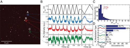
Fig. 2A shows a wide-field fluorescence image of hydroxylated NDs on the ITO working electrode under 532-nm excitation. The image was acquired using a 650-nm long-pass (LP) filter to preferentially detect NV− fluorescence. We applied triangular voltage sweeps between +0.75 and −0.75 V (Fig. 2B, Upper) while acquiring wide-field images with 100-ms exposure on an electron multiplying charge coupled device (emCCD) camera. From this series of images, we extracted the photoluminescence (PL) time traces of each fluorescent spot (Materials and Methods). Fig. 2B shows the PL recordings of the three characteristic spots highlighted in Fig. 2A. Individual traces are shown in the panel on the left, and voltage-cycle averaged PL traces (solid lines) with their SD (shaded region) are plotted on the right. From the cycle-averaged PL, we calculated the maximum PL modulation () and SD () for each spot. From these measurements, we determined the fraction of NVs with significant modulation, defined as . Of ∼4,300 NDs measured on multiple samples, 21 satisfied this metric of voltage-dependent PL modulation (Fig. 2C). The PL response is not uniform, but varies for different NDs. This nonuniform behavior is clear from the PL traces for the three sites shown in Fig. 2B: the PL of spots A and B increase at negative voltages, whereas the PL of spot C shows the opposite voltage dependence. To study this variation of PL modulation, we categorized the cycle-averaged PL into eight distinct types (types 1–8) shown on the left panel of Fig. 2D. The distribution of the subsets of NDs that exhibited voltage dependence is shown in Fig. 2D. Approximately 94% of detected spot PL modulation (types 1–3) were out of phase with respect to the applied potential and showed an increase in PL at negative potential differences, whereas 5% showed in-phase response (types 4–6). Some spots exhibited a PL change that was independent of the voltage polarity (types 7 and 8).
Fig. 2.
Wide-field fluorescence measurement results of hydroxylated NDs. (A) Typical wide-field fluorescence image of hydroxylated NDs on the ITO working electrode. (B) Fluorescence time traces of three different spots under repetitive triangular voltage sweep extracted from wide-field measurements. (Right) Average fluorescence (solid lines) and its SD (shaded region) for the eight voltage cycles. (C) Distribution of the maximum PL change () normalized to the SD of PL () for each measured fluorescent spot. Of the ∼4,300 different fluorescent spots, 21% showed PL modulation larger than 1.5 . (D) Statistical distribution of hydroxylated nanodiamond NV PL modulation due to the applied potential difference. PL modulation is categorized into eight types of voltage responses. The majority (93.8%) of the NV centers exhibit increased PL at negative voltages and decreased PL at positive voltages, corresponding to modulation types 1–3.
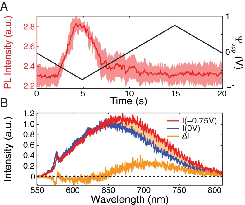
To investigate the role of the charge state in the PL modulation, we studied isolated NDs exhibiting single NV fluorescence, as determined by separate photon anti-bunching measurements showing g2 (SI Text). The cycle-averaged PL response of such a single NV is shown in Fig. 3A. This NV center exhibited the most common type 2 PL modulation, with a PL increasing 24 as the potential difference, , was lowered from 0 to −0.75 V. Fig. 3B shows the PL spectra for equal to 0 (blue line) and −0.75 V (red line), acquired with the confocal setup (Materials and Methods). The spectra of single NVs typically reflect rapidly switching NV0 and NV− charge states (5, 6). For = 0 V, the NV’s fluorescence spectrum exhibits dominant (75) NV0 emission with a 25 NV− contribution, as estimated from a fit (SI Text) to the NV− and NV0 spectra shown in Fig. 1A. The NV− contribution increases to at −0.75 V. The shaded region in Fig. 3B shows the difference between the two spectra above 650 nm. This difference corresponds to an increase of 31 above 650 nm, which approximately matches the 24% increase observed from the wide-field measurements (Fig. 3A). We conclude that for hydroxylated NDs, the voltage-dependent PL is primarily due to shifting of NV0 and NV− charge state distributions.
Fig. 3.
Voltage-dependent fluorescence of a single NV center in a hydroxylated ND. (A) Cycle-averaged mean PL response to applied potential difference, obtained from the wide-field data similar to Fig. 2B, for an isolated single NV center. (B) PL spectrum of the same NV center obtained at 0 V (blue) and at −0.75 V (red). The difference between the two spectra (orange shaded region) indicates that the NV− portion of the spectrum increases.
The change in the NV charge state can be qualitatively described by band bending due to electric field across the ND. Even without any applied external bias, the potential difference between the ITO and the Ag/AgCl electrodes due to their work function differences leads to the formation of a built-in electric field at the ITO/electrolyte interface. For the NV center in the hydroxylated ND shown in Fig. 3, this built-in electric field results in the ENV0/− level being slightly below EF and the NV primarily in the neutral charge state. The applied potential difference changes the electric field across the ND. This variation induces further band bending that reduces the energy separation between ENV0/− and EF at the position of the NV center, resulting in an increased probability of the NV to be in the negative charge state. The results shown in Figs. 2 and 3 indicate that for the majority of modulating NVs, lowering the potential of the ITO electrode with respect to the reference electrode increases the NV− contribution (modulation types 1–3). We attribute this imbalance in the voltage dependence to the built-in potential difference at the ITO/electrolyte interface. The distribution within the modulation types 1–3 is likely to be due to variations in the NV’s location in the ND and the ND’s shape. The band bending at the NV’s exact location depends on its distance to the surface, resulting in a range of responses to the same applied potential difference.
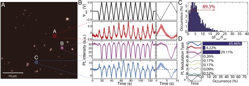
To investigate the influence of surface termination on the voltage-dependent ND PL, we repeated the above described experiments using NDs with hydrogenated surfaces (Materials and Methods and SI Text). Consistent with previous results of NVs near hydrogen-terminated surfaces (8), the PL of these NDs show predominantly NV0 emission due to the increase in the near-surface band bending. A 562-nm long-pass filter was used to detect changes in the NV0 fluorescence. The results, summarized in Fig. 4, were analyzed in the same manner as for the hydroxylated NDs (Fig. 2). Fig. 4B shows the PL for the three representative fluorescent spots indicated in Fig. 4A as is swept between +0.5 and −0.5 V. Remarkably, of the ∼1,200 distinct NDs measured across multiple samples, 89% showed an above-threshold PL modulation (Fig. 4C): a much larger percentage than for the hydroxylated NDs. In addition, these NDs also show a larger voltage dependence with a normalized PL () of up to 110 for a potential range of 0.75 to −0.75 V (SI Text). Moreover, the modulation characteristics (Fig. 4D) are more uniform (types 1–3) than for the hydroxylated NDs (Fig. 2D). This greater uniformity would be beneficial for sensing applications.
Fig. 4.
Wide-field fluorescence measurement results of hydrogenated NDs. (A) Typical wide-field fluorescence image of hydrogenated NDs on the ITO. (B) Fluorescence time traces of the different clusters of NDs indicated in A under repetitive triangular voltage sweep acquired with a 562 LP filter. (Right) Average fluorescence (solid lines) and its SD (shaded region) for the eight voltage cycles. (C) Distribution of the maximum PL change () normalized to the SD of PL () for each measured fluorescent spot. Of the ∼1,200 different NV NDs, 89% showed PL modulation larger than 1.5 . (D) Statistical distribution of hydrogenated ND NV PL modulation due to the applied potential difference. PL modulation is categorized into eight types of voltage responses. Among the ones that exhibited voltage dependence, almost all (>98%) show increased PL at negative voltages and decreased PL at positive voltages, corresponding to modulation types 1–3.
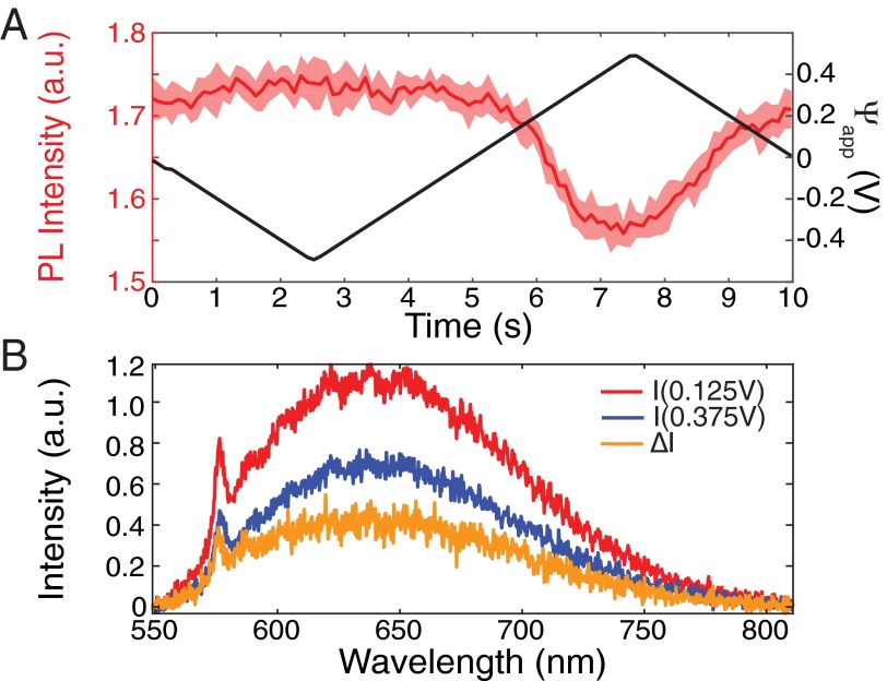
Fig. 5A shows the average PL change as a function of for an isolated hydrogenated ND containing a single NV center, as confirmed again by anti-bunching measurements (SI Text). As is increased, the NV PL drops, corresponding to modulation type 3 shown in Fig. 4. We also performed spectral measurements for an average of 125 and 375 mV, shown in the red and blue lines in Fig. 5B. The fluorescence spectra only show NV0 emission and negligible contribution from NV− for both bias voltages. Increasing the bias voltage decreases the NV0 fluorescence without any changes in the NV−. The observed decrease in NV0 could be either due to an increase in the nonradiative decay rate of the NV center or due to the switching of the NV center from the fluorescent NV0 to a nonfluorescent dark state that is commonly attributed to the NV+ charge state (14–16). A change in nonradiative decay rate would result in a change of NV excited state lifetime. However, we did not observe a significant change in fluorescence lifetime due to (SI Text). Therefore, we conclude that the PL variation is due to switching between the bright NV0 and the dark NV+ charge states with . Within the band bending picture, this indicates that applying a positive potential to the ITO increases band bending and pushes the ENV+/0 level further above EF.
Fig. 5.
Voltage-dependent fluorescence of a single NV center in a hydrogenated ND. (A) Cycle-averaged mean PL response to applied potential difference, obtained from the wide-field data similar to Fig. 4B, for an isolated single NV center. (B) PL spectrum of the same NV center obtained by applying a 250-mV amplitude square-wave voltage with a DC bias of 125 and 375 mV, corresponding to an average of 0.125 (blue) and 0.375 V (red), respectively. Both spectra show purely NV0 fluorescence, with the difference between the two showing that the PL change is due to a decrease in NV0 fluorescence.
We attribute the significant increase in the number of NV centers that show voltage-dependent PL in hydrogenated NDs to two effects: the large band-bending induced by hydrogen surface termination and the conductive properties of hydrogenated diamond surface. The NV charge state is determined by the position of the charge state transition levels ENV0/− and ENV+/0 with respect to EF inside the diamond. Hydrogen termination of the ND surfaces results in a stronger band bending compared with hydroxyl termination. The increased band bending accounts for the greater fraction of NV0 centers in hydrogen terminated diamond (Fig. 1B). The increase in the number of modulating NV centers therefore suggests that the average energy difference between ENV0/− and EF in hydroxylated NDs is larger than the average energy difference between ENV+/0 and EF in hydrogenated NDs. Thus, a larger external potential difference would be required to perturb the NV charge state in the hydroxylated NDs compared with hydrogenated NDs. Furthermore, unlike hydroxyl terminated diamond, hydrogen terminated diamond surfaces are conductive due to the formation of a surface hole accumulation layer (8). Consequently, charge transfer between the ITO electrode and hydrogenated NDs’ surface could occur. Such charge transfer to localized surface states would change the ND surface potential and affect the near-surface band bending. In addition, charging of the ND can also alter the Fermi level in the ND. Both of these effects will strongly influence the energy difference between ENV+/0 and EF, and thus NV’s charge state, which could result in an increased percentage of NVs demonstrating voltage-dependent PL.
To investigate the possibility of charge transfer, we repeated the wide-field measurements in Figs. 2 and 4 on ITO electrodes with a 5-nm-thick coating of alumina (Al2O3) acting as a spacer between the ITO and the NDs (Materials and Methods and SI Text). For hydroxylated NDs, we observe a decrease, from 23 to 13, in the number of NVs showing voltage-dependent PL, whereas for hydrogenated NDs, we observe a drastic decrease, from 89 to 1 (SI Text). These findings suggest that there are two different mechanisms by which the applied potential difference can modulate the charge state of the NV. For the hydroxylated NDs, the persistence of PL modulation in the presence of the alumina spacer suggests that the charge state modulation results from band-bending induced by the electric field generated by the potential difference across the ND. A similar electric field-induced effect has previously been observed in NV centers under the insulating regions of an in-plane field effect diamond device (15). However, for the hydrogenated NDs, almost no modulation was observed when the conductive diamond surface was not in direct electrical contact with the ITO electrode. This lack of modulation indicates that for hydrogenated NDs, band bending induced by charge transfer to the ND surface is the dominant mechanism by which the applied potential difference modulates the NV charge state. Although electric field-induced band bending could also occur for hydrogenated NDs on the alumina spacer layer, our results suggest that screening of the electric fields by the conductive surface surrounding the NDs reduces this effect.
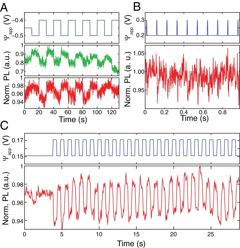
The sensitivity of the NV charge state and PL to external fields and potential changes could enable applications for sensing the local electrochemical environment, e.g., for neuronal voltage imaging. For hydroxylated NDs, the electric field due to the -mV variation in the neuron cell membrane potential could induce changes to the NV’s charge state and result in detectable PL modulation. One possible complication for this application is that the potential away from the cell membrane is rapidly screened due to the nanometer-scale Debye length in biological media. This challenge may be mitigated by using small (5–15 nm) NDs embedded inside the membrane. Our results indicate that the fluorescence of hydrogenated NDs is not directly sensitive to external electric fields but instead requires charge transfer to the ND surface to induce band bending, in agreement with previous studies on hydrogen terminated bulk diamond. Functionalizing the ND surface with charged molecules or polymers could provide a mechanism for such charge transfer. For example, it has been shown that electrical activity in cells can be detected by the use of voltage-dependent charge transfer from molecular wires to a fluorescent reporter (31, 32). Functionalizing hydrogenated NDs with similar molecular wires could provide the necessary charge movement and allow their use as voltage indicators. To gauge the expected performance of both hydroxylated and hydrogenated NDs, we tested their PL response to biologically relevant potential fluctuations at timescales that approach action potential in mammalian neurons using wide-field fluorescence imaging. Fig. 6A shows the PL intensity trace for two separate single NV centers in the hydroxylated NDs acquired with a camera exposure time of 100 ms. Both NVs exhibited clear PL modulation as a function of . We observed the strongest PL response when a bias voltage of −400 mV was applied to the modulation signal (see SI Text for the statistical distribution of DC bias point at which each NV showed the highest PL response). We also performed similar experiments on hydrogenated NDs. Because hydrogenated NDs are hydrophobic, they formed agglomerates on the hydrophilic ITO surface. Therefore, diffraction limited spots of hydrogenated NDs typically contained multiple NDs and NV centers, improving the signal to noise ratio of the measurement. Consequently, we were able to observe a clear PL response from individual clusters for voltage pulses as short as 5 ms and amplitude variations as small as 100 mV with a 2-ms camera exposure time (Fig. 6B). Shorter voltage pulses could not be detected due to the large RC time constant (5–30 ms) of the large surface area electrochemical cells used in this study. The time traces shown in Fig. 6 A and B are for individual fluorescent spots of NDs, with the green PL trace in Fig. 6A corresponding to the same single NV center as in Fig. 3. By integrating the signal of 12 distinct fluorescent spots across the image, 20-mV signals were detectable with a 33-ms exposure time (Fig. 6C).
Fig. 6.
Detection of small voltage variations. (A) PL time traces of two isolated hydroxylated NDs to 100-mV voltage changes. (B) PL time trace of a hydrogenated ND cluster to 5-ms, 100-mV square voltage pulses. (C) PL time trace of multiple ND clusters to 20-mV voltage changes.
Compared with optical voltage indicators that broadly stain cell membranes, sparse ND-based indicators could enable voltage recording from single subdiffraction limited sites and reduced background (33). In addition to the NV center, numerous other fluorescent defect centers in diamond and other semiconductor materials (e.g., SiC) have been investigated for quantum information and sensing applications (12, 34, 35). Such fluorescent defects can be stable in ultrasmall crystals: the SiV center has been observed in NDs as small as 1.6 nm in diameter (36). Many of these fluorescent defects are likely to also exhibit charge state and fluorescence modulation via the electrochemical environment.
In summary, we demonstrated the modulation of the charge state and fluorescence of NV centers in NDs in an electrochemical cell. The NV fluorescence response depends strongly on the ND surface termination, which affects both the underlying mechanism and the overall fraction of modulating NVs. For hydroxylated NDs, we observed shifting between the NV0 and NV− charge states. This charge state variation is attributed to changes in electric field induced band-bending inside the diamond in response to an applied potential difference. On the other hand, for hydrogenated NDs, we observe shifting of the NV charge state between NV0 and a nonfluorescent state. We attribute this switching mechanism to charge transfer between the NDs and the ITO electrode. Our results suggest the utility of NV-NDs for fluorescence-based sensing of electrochemical potential changes. Because of the strong PL modulation, which can be as high as Fmax/Fmean = 110%, it is possible to observe electric potential variations of 100 mV even with a single NV emitter. By collecting signal from several NVs, the detection of potential changes as low as 20 mV and a setup-limited temporal response down to 5 ms was achievable. This strong dependence of the NV charge state to the electrochemical environment promises an optical nanometer-scale sensing modality for the physical and life sciences.
Materials and Methods
Electrochemical Cell.
ITO-coated coverslips (30–60 /sq; SPI Supplies) were cleaned with acetone, isopropyl alcohol, and oxygen plasma. A cylindrical polypropylene tube was subsequently epoxied onto the ITO coverslip. This electrochemical cell contained 750 μL electrolyte at room temperature. The aqueous electrolyte consisted of 100 μM potassium chloride (KCl) with phosphate buffer (10 mM Na2PO4 and 1.8 mM KH2PO4) that stabilized the pH to 7.7. The NDs were deposited on the ITO coverslips from an aqueous solution or toluene and heated to remove the solvent. The NDs were derived from high-pressure high-temperature (HPHT) diamond and were irradiated and annealed to induce NV centers. The mean sizes of the hydroxylated and hydrogenated diamonds are 18 ± 8 and 12 ± 5 nm, respectively [see SI Text for transmission electron microscopy (TEM) analysis]. The surface termination moieties were confirmed by FTIR (SI Text). The electrochemical potentials were applied using a potentiostat (CH Instruments; 630D) in a three-electrode setup consisting of the ITO working electrode, a platinum wire (CH Instruments) counter electrode, and a leak-free reference electrode (Harvard Apparatus). The alumina (Al2O3)-coated ITO working electrode was fabricated by deposition of 5 nm alumina with atomic layer deposition.
Experimental Setup.
The experiments were performed on an inverted microscope (Zeiss Axiovert 200M) equipped with an immersion oil objective (Zeiss Planapochromat 100× NA = 1.4). For wide-field fluorescence measurements, a 300-mW, 532-nm continuous wave (CW) laser was focused to the back aperture of the objective to illuminate an 42-μm-diameter area on the electrochemical cell. The fluorescence signal from NV centers was collected with the same objective, filtered using either a 562- or 650-nm long-pass filter, and imaged on an emCCD camera (Photometrics Cascade 1k, Photometrics 128+, and Hamamatsu C9100-13). The synchronization of the potentiostat voltage and the camera frames was performed with a data acquisition board (NI-DAQ 6553). The voltage-dependent PL recordings of each fluorescent spot were obtained by the analysis of the wide-field measurements using custom MATLAB routines. Confocal measurements were performed with a home-built laser scanning microscopy setup implemented on the side port of the same microscope. In short, the 532-nm excitation laser focused to a diffraction limited spot was scanned on the sample surface using two galvanometer mirrors located on a plane conjugate to the microscope objective back aperture. The fluorescence signal was collected with the same path, spectrally filtered with either a 550-nm long-pass or a 550- to 600-nm band-pass filter, and imaged on a single mode optical fiber connected to a single avalanche photodiode (APD) or spectrometer. Spectral measurements were performed by connecting the collection fiber to a grating spectrometer (SP2500i; Princeton Instruments) equipped with a CCD camera (PIXIS 1024B; Princeton Instruments). Note that the fast oscillations observed in the spectra shown in Figs. 1A, 3B, and 5B are due to the etaloning effect on the CCD camera.
SI Text
Band Bending-Induced NV Charge State Shifting in NDs.
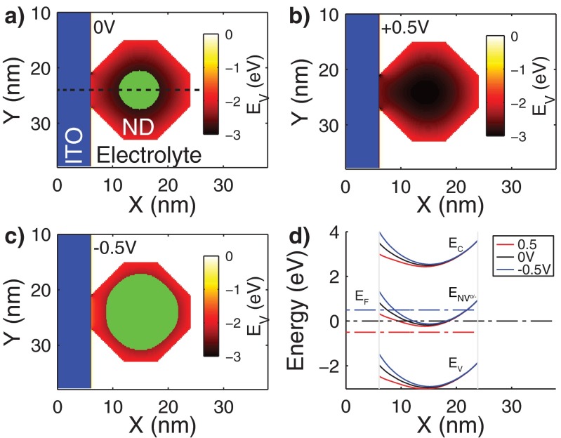
Previous work by Grotz et al. (14) investigated variations of the charge state of NV centers located near the surface of a bulk diamond in contact with an electrolyte. This study used numerical modeling using the nextnano numerical simulation package, which can self-consistently solve for the coupled Schrodinger-Poisson equation (37, 38). We used the same software package to calculate the energy band structure of the ITO/ND/electrolyte system and to investigate how a potential difference applied between the ITO working electrode and the reference electrode affects the band bending inside the ND and the NV charge state. Specifically, we performed 2D simulations of an 18-nm ND in contact with an ITO working electrode (modeled as a metal) and surrounded by an electrolyte (Fig. S1A). The simulation parameters for the diamond are as follows (14): T = 298 K; diamond band gap = 5.47 eV; valence band masses = 2.18, 0.7, and 1.06 m0; nitrogen concentration = 100 ppm; NV0/− charge state transition level, ENV0/− = 2.8 eV + EV; electrolyte = 10 mM phosphate buffer with 100 μM KCl.
Fig. S1.
Numerical simulation result of the energy band diagram of the ITO/nanodiamond/electrolyte system. 2D map of the valence band maxima for (A) 0, (B) +0.5, and (C) −0.5 V. The regions for which ENV0/− < EF are highlighted in green. (D) Energy band diagram of the cross-section highlighted in A for the three applied potential differences.
Fig. S1A shows the calculated 2D map of the valence band maxima with respect to the reference electrode at 0 V. As discussed in the main text, the charge state of an NV center depends on the energy difference between the charge state transition level (ENV0/−) and the Fermi level (EF) (see Fig. 1B and related discussion). The green area in Fig. S1A shows the region for which ENV0/− < EF. An NV center located within this region would be in the negative charge state. As the voltage applied to the working electrode is varied, the energy separation between ENV0/− and EF changes. At +0.5 V (Fig. S1B), as ENV0/− is above EF throughout the ND, the NVs are in the neutral charge state. At −0.5 V, on the other hand, ENV0/− crosses below EF for a significant portion of the ND, and a higher percentage of NVs is in the negative charge state (green area in Fig. S1C). The diamond energy band diagram for the horizontal cross-section delineated with the dashed line in Fig. S1A for all three applied potential differences is shown in Fig. S1D. These simulations qualitatively show how the applied potential difference modifies the NV charge state. It should be noted, however, that these simulations do not capture all of the complexities arising from the multiple NV facets, surface groups, ND size, etc.
ND Surface and Size Characterization.
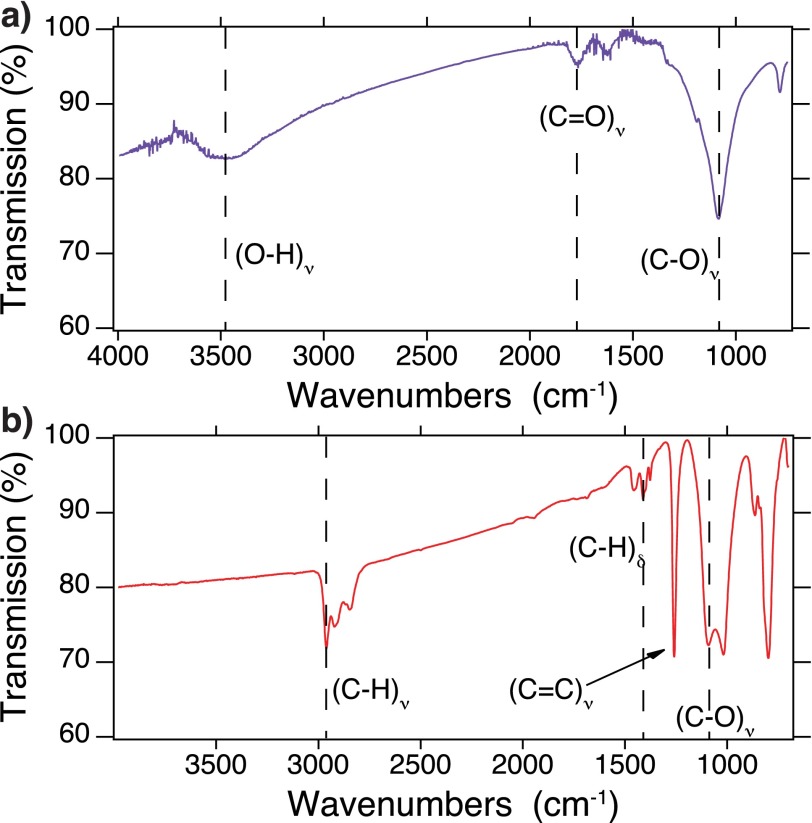
We studied the voltage dependence of two types of NDs with different surface termination groups. Fig. S2 shows the FTIR transmission spectra of hydroxylated and hydrogenated NDs. The ND type identified as hydroxylated NDs in the main text have a surface structure that includes both carboxylic acid (-COOH) and alcohol (-OH) moieties (Fig. S2A) (30). On the other hand, the hydrogenated NDs (Fig. S2B) have strong stretching (C-H)ν modes from 2,800 to 2,900 cm−1 and weaker bending modes (C-H)δ from 1,360 to 1,500 cm−1 (39). Carbon-oxygen moieties are still present as evidenced by (C-O)ν at 1,100 cm−1, whereas the acid vibration is no longer present.
Fig. S2.
FTIR spectra of (A) the hydroxylated nanodiamonds and (B) hydrogenated nanodiamonds. (A) (O-H)ν modes on the diamond surface are observed at 2,700–3,500 cm−1 due to adsorbed water, whereas the (O-H)δ can be seen at 1,640 cm−1. The (C = O)ν mode at 1,780 cm−1 and (C-O)ν at 1,100 cm−1 is still observed due to acids and alcohols. (B) (C-H)ν modes on the ND surface are observed at 2,800–2,900 cm−1, whereas the (C-H)δ can be seen at 1,360–1,500 cm−1. The (C-O)ν mode at 1,100 cm−1 is still observed due to alcohols, whereas a sharp mode at 1,260 cm−1 is believed to be (C = C)ν.
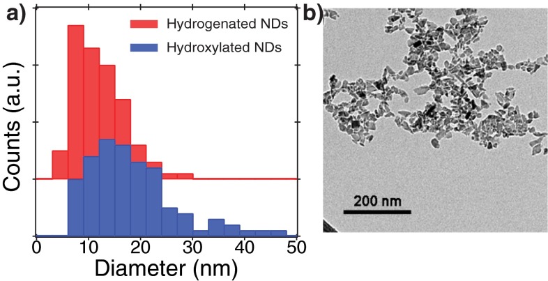
The size distribution of the two types of NDs was characterized by TEM. TEM analysis of the hydroxylated and hydrogenated NDs used in this study are not statistically distinct. For TEM analysis, the samples were deposited from colloidal solutions (10 μg/mL) onto holey carbon-coated Cu grids (Ted Pella; 01824) and imaged on a FEI Tecnai Spirit microscope operating at 120 keV. Images were analyzed using the ImageJ software package. The area of individual particles was measured using a free-hand drawing tool, and a sample set of 100 particles was analyzed. The diameter was estimated by assuming a spherical particle of cross-sectional area . Histograms of the ND diameter for the two samples (Fig. S3) were generated for bin sizes of 3 nm and a total of 25 bins. Both average and SD were calculated directly from the 100 NDs sampled for each of the two samples.
Fig. S3.
(A) Histograms of the diameters of the two types of HPHT NDs used in this study. The histograms were generated from size measurements of TEM images taken from each sample. The hydrogenated NDs have size of 12 ± 5 nm and the hydroxylated NDs have a size of 18 ± 8 nm, based on a 100 ND ensemble. The size was estimated from the TEM analysis with a spherical particle shape model as described in the procedure. (B) A representative TEM image.
Single NV in Hydroxylated ND.
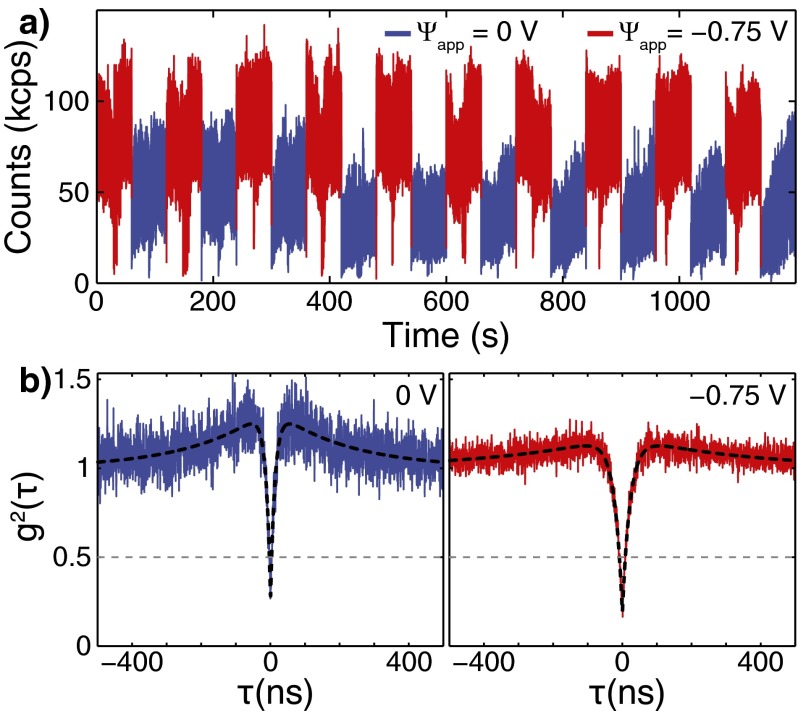
To confirm that the observed voltage dependent fluorescence signal and charge state shifting shown in Fig. 3 originate from a single NV center in a hydroxylated ND, we measured the second-order autocorrelation as a function of applied potential difference (). Using a fiber based Hanbury-Brown-Twiss (HBT) setup, we recorded the photon arrival times on two APDs using the time-tagging mode of a PicoHarp 300 time-correlated single photon counting system. At the same time, the electrochemical potential was varied between two voltages every 60 s. Fig. S4A shows the total count rate on both APDs while the is varied between the low PL state at 0V (red) and the high PL state at −0.75V (blue). To compensate for sample drift, the confocal spot was readjusted every 60 s to the maximal PL signal position, which resulted in the PL dips observed in the middle of each voltage cycle. The second-order autocorrelation results [] obtained from the photon arrival times for the two different values are shown in Fig. S4B without background subtraction. The results show the anti-bunching at zero delay and bunching at short delay times typically observed for NV centers. Most importantly, the anti-bunching dip at reaches 0.27 and 0.17, respectively, for 0 and −0.75 V. The shows that the PL signal is due to a single NV center and that an additional emitter is not being turned on or off due to the applied potential difference.
Fig. S4.
(A) Fluorescence time trace measurements for the same NV center for a rectangular voltage signal acquired with a fiber-based confocal HBT setup. (B) Second-order autocorrelation result obtained from the analysis of photon arrival times at two different values shown in A.
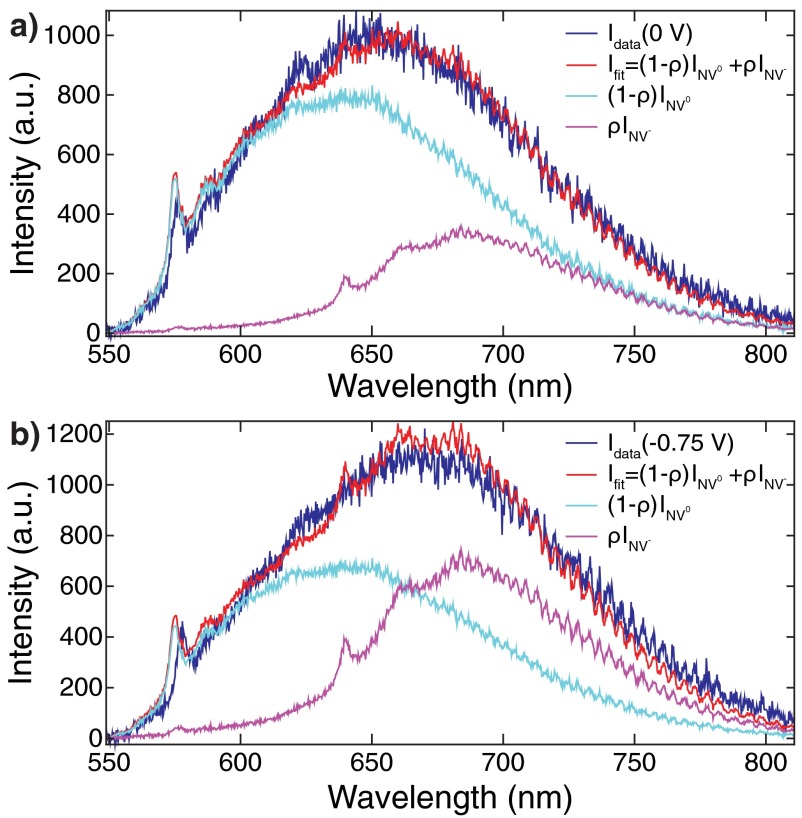
As discussed in the main text, we recorded the PL spectrum of an NV center in a hydroxylated ND for two different values (Fig. 3). The single NV center’s spectrum exhibited PL signal from both NV0 and NV−. To quantify the PL contribution from each NV charge state, we fit the PL spectra at each (blue lines, Fig. S5) to a linear superposition of the NV0 and NV− spectra shown Fig. 1A using . From these fits (red lines) we deduce that the NV− contribution, ρ, increases from at 0 V (Fig. S5A) to at V. We notice that the position of the NV0 zero-phonon-line (ZPL) acquired at the two voltages does not match that of the reference spectrum perfectly. Furthermore, the ZPL shifts from 575.9 nm at 0 V (Fig. S5A) to 577.6 nm at −0.75 V (Fig. S5B), which is indicative of a large DC Stark shift. To first order, the linear Stark shift of an electronic transition () due to a local electric field (F) is given by . Although there has been no systematic study of DC Stark shift of the NV0 ZPL, studies on NV− have obtained of up to 1.5 Debye. Assuming that the NV0 would exhibit a similar dipole moment change, the 1.7-nm ZPL shift we observe indicates a local electric field on the order of V/m. This value is on the same order of magnitude as the electric field due to the electrochemically applied potential change of 0.75 V dropping over a Debye length of nm.
Fig. S5.
Fitting of the PL spectra at 0 (A) and −0.75 V (B) to the linear combination of NV0 and NV− reference spectra shown in Fig. 1.
Single NV in Hydrogenated ND.
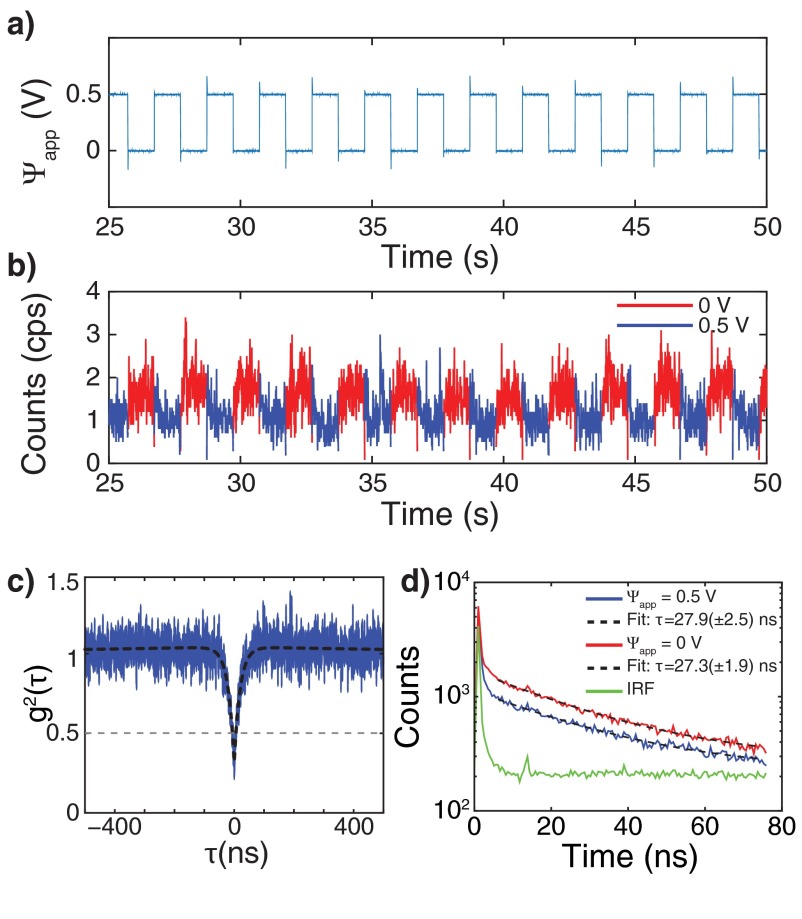
Fig. 5B shows the PL spectra for a single NV0 center in a hydrogenated ND. The single emitter nature of the NV center was confirmed by second-order autocorrelation measurements (Fig. S6C). The applied potential difference () affects the NV0 PL intensity only, and no contribution from the NV− state is observed. The change in the NV0 PL can be attributed to the transition of the NV center from the neutral NV0 to the nonfluorescent positively charged NV+ state that has been recently reported in bulk diamond (14, 15). Another potential cause of the PL modulation in hydrogenated NDs is the voltage-dependent variations on the nonradiative decay processes. For a single emitter, the PL intensity is directly proportional to the quantum efficiency (QE), which depends on the radiative () and nonradiative () decay rates: . Consequently, an increase in the nonradiative decay rate would result in reduced PL intensity. Variations in the nonradiative decay rate would also result in different excited state lifetimes (τ) as . We performed time-resolved PL measurements on the NV0 fluorescence to obtain the lifetime at different values. To this end, the NV center was excited using a pulsed supercontinuum laser (superK Extreme; NKT Photonics) whose output was filtered with a 10-nm band-pass filter centered at 532 nm. The 78-MHz pulse repetition rate was reduced to 13 MHz using an electro-optic modulator-based pulse picker setup. Periodic square-wave voltage pulses of 0.5 V were applied (Fig. S6A), whereas the PL signal from NV0 was detected with a single APD and time-tagged with respect to the laser pulse using a time-correlated single photon counting system (PicoHarp 300). The time-tagged photons arrival events were then used to obtain both the PL count rate (Fig. S6B) and PL decay traces (Fig. S6D). The PL decay traces were fit to a single exponential decay, , to obtain the excited state lifetime. Fig. S6D shows two PL decay traces obtained at 0 (red) and +0.5 V (blue). The corresponding fits (dashed lines) show that the lifetime stays constant at ∼27 ns, even though the PL count rate decreases as seen in Fig. S6B. This constant lifetime indicates that nonradiative decay processes do not play a significant role in the voltage-dependent PL. We thus conclude that the PL variation is due to switching between the fluorescent NV0 and the nonfluorescent NV+ charge states.
Fig. S6.
Single NV in hydrogenated nanodiamond lifetime analysis. Applied potential difference (A) and corresponding PL time traces (B) of a single NV center as determined from second-order autocorrelation measurements (C). PL decay traces (D) at 0 (red) and 0.5 V (blue) together with the instrument response function (IRF) and the fits to decay traces (dashed lines).
Voltage-Dependent PL Statistics.
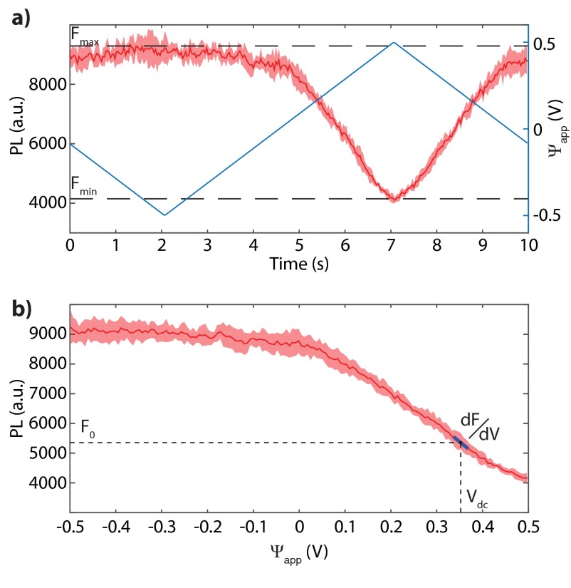
We observed variations in the voltage-dependent PL modulation for both hydroxylated and hydrogenated NDs. From wide-field measurements (similar to Figs. 2 and 4), we obtain the PL recordings as a function of the applied potential difference for each fluorescent spot by averaging the signal over a circle of five pixels in diameter (Figs. 2B, Left, and 4B, Left). We then average the PL signal over the periodically repeated voltage cycles. Fig. S7A shows an example of the cycle-averaged PL (solid red line) and its SD (shaded red area) for one voltage cycle. As discussed in the main text, we label a fluorescent spot as having a voltage dependent PL if the maximal PL change () is larger than 1.5 times the SD of the PL signal (). With this threshold definition, we observed that, compared with the hydroxylated NDs, a significantly higher percentage (89) of the hydrogenated NDs showed voltage-dependent PL (Figs. 2C and 4C). From the PL recordings we also calculate the average PL as a function of (Fig. S7B), which we used to identify the DC bias voltage at which the differential PL change () was the highest.
Fig. S7.
Example cycle-averaged PL data as a function of time (A) and as function (B).
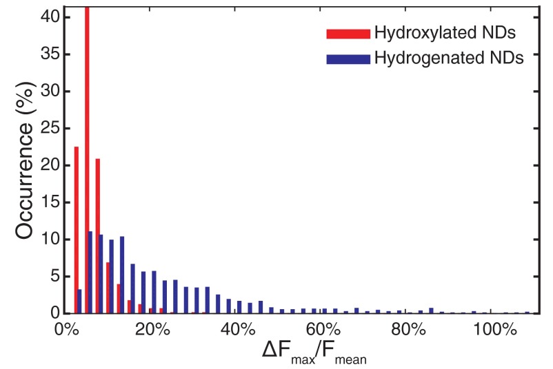
After identifying all of the spots showing PL modulation, we first sought to quantify the response of the PL change to the applied potential difference for each fluorescent spot. Fig. S8 shows the distribution of the modulation depth, defined as the maximum PL change () normalized to the mean PL signal of that spot [], for both hydroxylated and hydrogenated NDs.
Fig. S8.
Statistical distribution of the modulation depth for each fluorescent spot for hydroxylated (red) and hydrogenated (blue) ND samples.
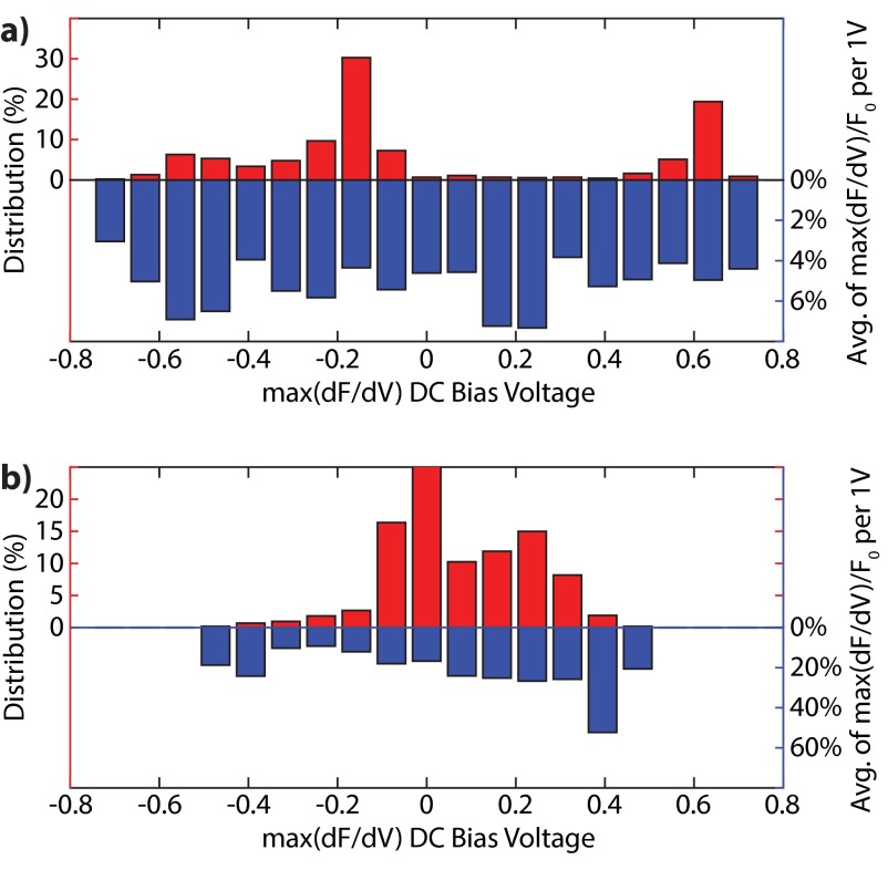
As shown in the PL time traces in Fig. S7, as well as Figs. 2B and 4B, the relation between the PL signal and applied potential difference is not linear. For example, in Fig. 4B, the spot highlighted in red shows large PL change at negative and little variation at positive , whereas the opposite is true for the spot highlighted in purple. To characterize such differences, we identified the bias voltage () for which the PL change for an applied potential difference was at a maximum [i.e., ] (Fig. S7). Fig. S9 shows the distribution of the DC bias voltages for (A) hydroxylated and (B) hydrogenated NDs, and the normalized to , which is the fluorescence intensity averaged over each modulating spot at that DC bias voltage value (Fig. S7).
Fig. S9.
Analysis of the distribution of the DC bias voltages for (A) hydroxylated and (B) hydrogenated NDs, together with the average normalized to at each DC bias voltage value.
Alumina-Coated ITO Working Electrode Results.
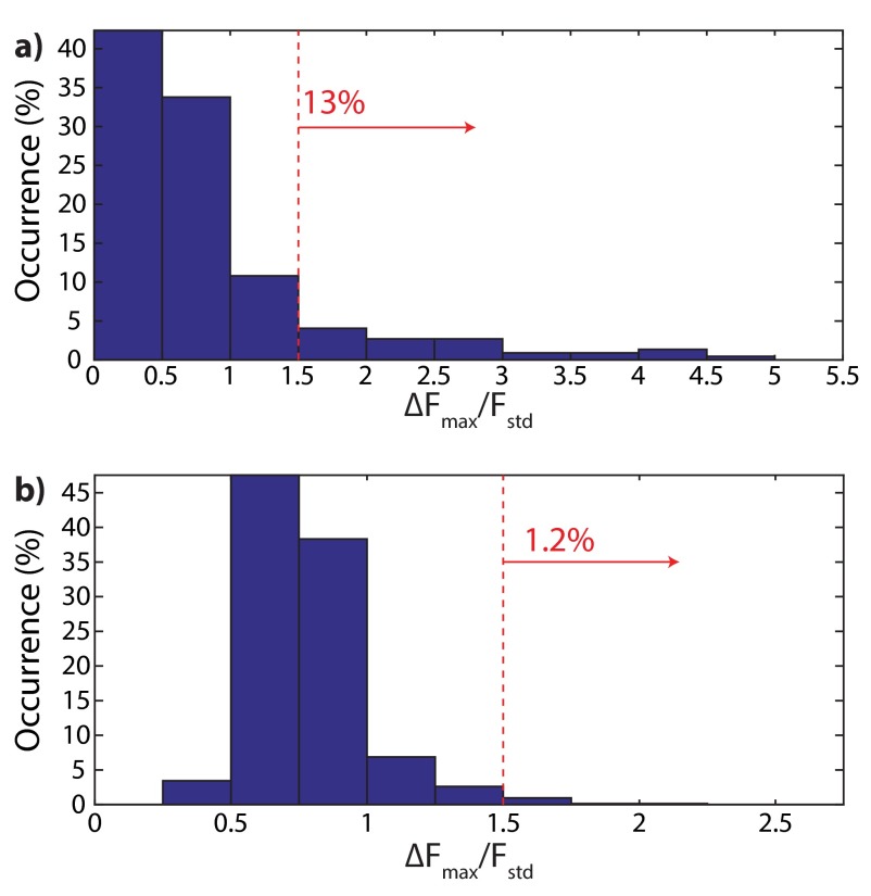
To study the possibility of charge transfer between the ITO working electrode and the ND surface, we repeated the experiments summarized in Figs. 2 and 4 with ITO working electrodes coated with 5 nm Al2O3 using atomic layer deposition. Fig. S10 shows the maximum PL change () normalized to the SD of the PL signal () for (A) hydroxylated and (B) hydrogenated NDs. For hydroxylated NDs, we observe a decrease, from 23% to 13%, in the number of NVs showing voltage dependence, whereas for hydrogenated NDs, we observe a more significant decrease (from 89% to 1%).
Fig. S10.
Distribution of the maximum PL change () normalized to the SD of PL () for each measured fluorescent spot in (A) hydroxylated and (B) hydrogenated NDs on 5 nm Al2O3-coated ITO electrodes. (A) For hydroxylated NDs, 13% of 222 measured fluorescent spots showed PL change larger than 1.5 . (B) For hydrogenated NDs, 1.2% of 728 measured fluorescent spots showed PL change larger than 1.5 .
Acknowledgments
We thank Igal Bayn for fabricating the Al2O3-coated samples and Tim Schröder, Florian Dolde, Edward H. Chen, Matthew E. Trusheim, Wieteke de Boer, Adam Gali, Kohei Itoh, Jose Garrido, and Jonathan Hodges for helpful discussions. Financial support was provided in part by the McGovern Institute Neurotechnology Program, the W. M. Keck Foundation, Army Research Office (ARO) Multidisciplinary University Research Initiatives (MURI) Grant W911NF-12-1-0594, Simons Foundation, Jeremy and Joyce Wertheimer, National Institutes of Health (NIH) Grant 1R01NS087950, Diamond Nanotechnologies Defense Advanced Research Projects Agency (DARPA) Grant D14PC00121, DARPA Grant HR0011-14-C-0018, and NIH Grant 1R43MH102942-01. R.S. was supported by a National Science Foundation Graduate Research Fellowship under Grant 1122374.
Footnotes
The authors declare no conflict of interest.
This article is a PNAS Direct Submission. F.J. is a guest editor invited by the Editorial Board.
This article contains supporting information online at www.pnas.org/lookup/suppl/doi:10.1073/pnas.1504451113/-/DCSupplemental.
References
- 1.Tamarat P, et al. Stark shift control of single optical centers in diamond. Phys Rev Lett. 2006;97(8):083002. doi: 10.1103/PhysRevLett.97.083002. [DOI] [PubMed] [Google Scholar]
- 2.Bassett LC, Heremans FJ, Yale CG, Buckley BB, Awschalom DD. Electrical tuning of single nitrogen-vacancy center optical transitions enhanced by photoinduced fields. Phys Rev Lett. 2011;107(26):266403. doi: 10.1103/PhysRevLett.107.266403. [DOI] [PubMed] [Google Scholar]
- 3.Dolde F, et al. Electric-field sensing using single diamond spins. Nat Phys. 2011;7(6):459–463. [Google Scholar]
- 4.Maze JR, et al. Nanoscale magnetic sensing with an individual electronic spin in diamond. Nature. 2008;455(7213):644–647. doi: 10.1038/nature07279. [DOI] [PubMed] [Google Scholar]
- 5.Gaebel T, et al. Photochromism in single nitrogen-vacancy defect in diamond. Appl Phys B. 2006;82(2):243–246. [Google Scholar]
- 6.Aslam N, Waldherr G, Neumann P, Jelezko F, Wrachtrup J. Photo-induced ionization dynamics of the nitrogen vacancy defect in diamond investigated by single-shot charge state detection. New J Phys. 2013;15(1):013064. [Google Scholar]
- 7.Fu KMC, Santori C, Barclay PE, Beausoleil RG. Conversion of neutral nitrogen-vacancy centers to negatively charged nitrogen-vacancy centers through selective oxidation. Appl Phys Lett. 2010;96(12):121907. [Google Scholar]
- 8.Hauf MV, et al. Chemical control of the charge state of nitrogen-vacancy centers in diamond. Phys Rev B. 2011;83(8):081304. [Google Scholar]
- 9.Rutter MJ, Robertson J. Ab initio calculation of electron affinities of diamond surfaces. Phys Rev B. 1998;57(15):9241–9245. [Google Scholar]
- 10.Sque SJ, Jones R, Briddon PR. Structure, electronics, and interaction of hydrogen and oxygen on diamond surfaces. Phys Rev B. 2006;73(8):085313. [Google Scholar]
- 11.Futera Z, Watanabe T, Einaga Y, Tateyama Y. First principles calculation study on surfaces and water interfaces of boron-doped diamond. J Phys Chem C. 2014;118(38):22040–22052. [Google Scholar]
- 12.Weber JR, et al. Quantum computing with defects. Proc Natl Acad Sci USA. 2010;107(19):8513–8518. doi: 10.1073/pnas.1003052107. [DOI] [PMC free article] [PubMed] [Google Scholar]
- 13.Deák P, Aradi B, Kaviani M, Frauenheim T, Gali A. Formation of NV centers in diamond: A theoretical study based on calculated transitions and migration of nitrogen and vacancy related defects. Phys Rev B. 2014;89(7):075203. [Google Scholar]
- 14.Grotz B, et al. Charge state manipulation of qubits in diamond. Nat Commun. 2012;3(729):729. doi: 10.1038/ncomms1729. [DOI] [PMC free article] [PubMed] [Google Scholar]
- 15.Hauf MV, et al. Addressing single nitrogen-vacancy centers in diamond with transparent in-plane gate structures. Nano Lett. 2014;14(5):2359–2364. doi: 10.1021/nl4047619. [DOI] [PubMed] [Google Scholar]
- 16.Schreyvogel C, Wolfer M, Kato H, Schreck M, Nebel CE. Tuned NV emission by in-plane Al-Schottky junctions on hydrogen terminated diamond. Sci Rep. 2014;4:3634. doi: 10.1038/srep03634. [DOI] [PMC free article] [PubMed] [Google Scholar]
- 17.Kato H, et al. Tunable light emission from nitrogen-vacancy centers in single crystal diamond PIN diodes. Appl Phys Lett. 2013;102(15):151101. [Google Scholar]
- 18.Doi Y, et al. Deterministic electrical charge-state initialization of single nitrogen-vacancy center in diamond. Phys Rev X. 2014;4(1):011057. [Google Scholar]
- 19.Kucsko G, et al. Nanometre-scale thermometry in a living cell. Nature. 2013;500(7460):54–58. doi: 10.1038/nature12373. [DOI] [PMC free article] [PubMed] [Google Scholar]
- 20.McGuinness LP, et al. Quantum measurement and orientation tracking of fluorescent nanodiamonds inside living cells. Nat Nanotechnol. 2011;6(6):358–363. doi: 10.1038/nnano.2011.64. [DOI] [PubMed] [Google Scholar]
- 21.Mohan N, Chen CS, Hsieh HH, Wu YC, Chang HC. In vivo imaging and toxicity assessments of fluorescent nanodiamonds in Caenorhabditis elegans. Nano Lett. 2010;10(9):3692–3699. doi: 10.1021/nl1021909. [DOI] [PubMed] [Google Scholar]
- 22.Rittweger E, Han KY, Irvine SE, Eggeling C, Hell SW. Sted microscopy reveals crystal colour centres with nanometric resolution. Nat Photonics. 2009;3(3):144–147. [Google Scholar]
- 23.Maurer PC, et al. Far-field optical imaging and manipulation of individual spins with nanoscale resolution. Nat Phys. 2010;6(11):912–918. [Google Scholar]
- 24.Chen EH, Gaathon O, Trusheim ME, Englund D. Wide-field multispectral super-resolution imaging using spin-dependent fluorescence in nanodiamonds. Nano Lett. 2013;13(5):2073–2077. doi: 10.1021/nl400346k. [DOI] [PubMed] [Google Scholar]
- 25.Balasubramanian G, et al. Nanoscale imaging magnetometry with diamond spins under ambient conditions. Nature. 2008;455(7213):648–651. doi: 10.1038/nature07278. [DOI] [PubMed] [Google Scholar]
- 26.Schrand AM, et al. Are diamond nanoparticles cytotoxic? J Phys Chem B. 2007;111(1):2–7. doi: 10.1021/jp066387v. [DOI] [PubMed] [Google Scholar]
- 27.Hall LT, et al. Monitoring ion-channel function in real time through quantum decoherence. Proc Natl Acad Sci USA. 2010;107(44):18777–18782. doi: 10.1073/pnas.1002562107. [DOI] [PMC free article] [PubMed] [Google Scholar]
- 28.Cooper A, Magesan E, Yum HN, Cappellaro P. Time-resolved magnetic sensing with electronic spins in diamond. Nat Commun. 2014;5:3141. doi: 10.1038/ncomms4141. [DOI] [PubMed] [Google Scholar]
- 29.Chao JI, et al. Nanometer-sized diamond particle as a probe for biolabeling. Biophys J. 2007;93(6):2199–2208. doi: 10.1529/biophysj.107.108134. [DOI] [PMC free article] [PubMed] [Google Scholar]
- 30.Wolcott A, et al. Surface structure of aerobically oxidized diamond nanocrystals. J Phys Chem C Nanomater Interfaces. 2014;118(46):26695–26702. doi: 10.1021/jp506992c. [DOI] [PMC free article] [PubMed] [Google Scholar]
- 31.Miller EW, et al. Optically monitoring voltage in neurons by photo-induced electron transfer through molecular wires. Proc Natl Acad Sci USA. 2012;109(6):2114–2119. doi: 10.1073/pnas.1120694109. [DOI] [PMC free article] [PubMed] [Google Scholar]
- 32.Woodford CR, et al. Improved PeT molecules for optically sensing voltage in neurons. J Am Chem Soc. 2015;137(5):1817–1824. doi: 10.1021/ja510602z. [DOI] [PMC free article] [PubMed] [Google Scholar]
- 33.Peterka DS, Takahashi H, Yuste R. Imaging voltage in neurons. Neuron. 2011;69(1):9–21. doi: 10.1016/j.neuron.2010.12.010. [DOI] [PMC free article] [PubMed] [Google Scholar]
- 34.Aharonovich I, et al. Diamond-based single-photon emitters. Rep Prog Phys. 2011;74(7):076501. [Google Scholar]
- 35.Falk AL, et al. Electrically and mechanically tunable electron spins in silicon carbide color centers. Phys Rev Lett. 2014;112(18):187601. doi: 10.1103/PhysRevLett.112.187601. [DOI] [PubMed] [Google Scholar]
- 36.Vlasov II, et al. Molecular-sized fluorescent nanodiamonds. Nat Nanotechnol. 2014;9(1):54–58. doi: 10.1038/nnano.2013.255. [DOI] [PubMed] [Google Scholar]
- 37.Birner S, et al. nextnano: General purpose 3-D simulations. IEEE Trans Electron Dev. 2007;54(9):2137–2142. [Google Scholar]
- 38.Trellakis A, et al. The 3D nanometer device project nextnano: Concepts, methods, results. J Comput Electron. 2007;5(4):285–289. [Google Scholar]
- 39.Ando T, et al. Fourier-transform infrared photoacoustic studies of hydrogenated diamond surfaces. J Chem Soc, Faraday Trans. 1993;89(4):749–751. [Google Scholar]


