Abstract
Single layers of MoS2 and MoSe2 were optically pumped with circularly polarized light and an appreciable polarization was initialized as the pump energy was varied. The circular polarization of the emitted photoluminescence was monitored as a function of the difference between the excitation energy and the A-exciton emission at the K-point of the Brillouin zone. Our results show a threshold of twice the LA phonon energy, specific to the material, above which phonon-assisted intervalley scattering causes depolarization. In both materials this leads to almost complete depolarization within ~100 meV above the threshold energy. We identify the extra kinetic energy of the exciton (independent of whether it is neutral or charged) as the key parameter for presenting a unifying picture of the depolarization process.
Materials often exhibit fundamentally new phenomena in reduced dimensions, and the new properties that emerge can lead to novel applications. Like graphite, the molybdenum-based transition metal dichalcogenides, MoX2 (X = S, Se) are a class of materials that readily lend themselves to dimensional manipulation. These layered structures have strong intralayer bonding and weak interlayer van der Waals coupling, enabling one to isolate individual layers. In bulk form, MoX2 are indirect gap semiconductors. However, because of their reduced dimensionality, single layers are direct-gap with a range of bandgaps in the visible regime. This makes them ideal candidates for a host of optoelectronic applications ranging from light-emitting diodes to light harvesting to sensors1,2,3,4,5. Besides the obvious light-based applications, these materials are also good candidates for the emerging field of valleytronics6,7,8,9,10,11,12. The reduced-dimensional, hexagonal lattice leads to non-degenerate K-points in the Brillouin zone making the inequivalent K and K’ valley populations potential new state-variables of these systems.
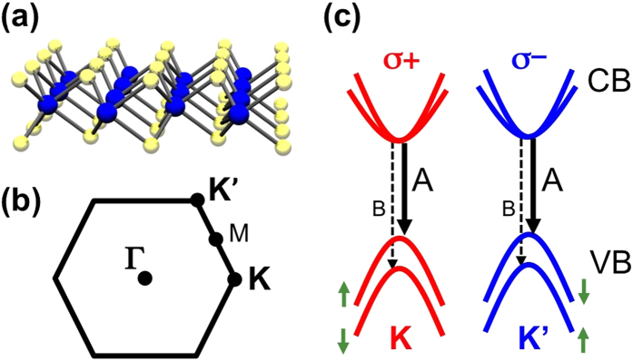
A single layer of MoX2, schematically shown in Fig. 1(a), consists of a plane of transition metal atoms sandwiched by layers of chalcogen atoms. The Brillouin zone of this system is shown in Fig. 1(b). In single layer form, the direct gap occurs at the K-point, and the optical properties of these materials are governed by strong excitonic transitions, both neutral and charged. These excitons are strongly bound, with the neutral exciton having binding energies on the order of 0.5–0.8 eV13,14,15,16,17 and the charged exciton (trion) having a binding energy of 20–30 meV9,18. In addition to being optically active with strong photoluminescence (PL), they also have unique optical selection rules (Fig. 1(c)). Time reversal symmetry and strong orbital-hybridization couples the valley and spin indices. This enables access to a single valley using polarized light, since the angular momentum of incident circularly-polarized light interacts with carriers to produce specific spin states8,9,10,11,19,20. In other words, the symmetry properties of the two inequivalent valleys lead to a difference in the absorption of circularly polarized light, either positive (σ+) or negative (σ−) helicity, resulting in a strong chiral selectivity.
Figure 1. Structure of Monolayer MoS2.
(a) Crystal structure of a single-layer transition-metal dichalcogenide. A central layer of transition metal atoms is sandwiched by layers of chalcogens. (b) Brillouin zone for a reduced dimensional hexagonal lattice. Some relevant high symmetry points are indicated. (c) Schematic of the single-particle band structure at K and K’ valleys. The arrows denote the A (solid line) and B (dashed line) excitons. Each valley can only be excited with a specific helicity, σ+ or σ−.
Polarization-resolved photoluminescence of single layer MoS2 has been extensively studied, and a high initial circular polarization was reported with a circularly polarized pump8,19. In contrast, there are few polarization-dependent studies for MoSe2 at zero magnetic field. One recent study21 reported very low initial circular polarization in the PL. This result is surprising since one expects members of the MoX2 family to behave similarly. Several other recent studies22,23, demonstrated generation of valley polarization in MoSe2 by applying external magnetic fields up to 10 T perpendicular to the sample. In particular, MacNeil et al.22 observed a maximum polarization of 14% for the charged and 9% for the neutral exciton at 4.2 K and 6.7 T attributed to the magnetic field breaking the K/K’ valley-degeneracy.
In this work, we measure the energy-dependent valley polarization in both MoS2 and MoSe2 under zero magnetic field, and model the polarization relaxation. We probe the valley population dynamics in MoSe2 and MoS2 by selectively populating the K and K’ valleys with circularly polarized light while systematically varying the laser excitation energy. For both systems, the difference in the excitation energy and PL emission energy, ΔE = Epump − EPL, governs the depopulation of carriers in each valley. Adding more energy above a distinct threshold characteristic of the longitudinal acoustic (LA) phonon for each material enables inter-valley scattering and produces a sharp decrease in the observed circular polarization. LA phonons in these two systems have different energies (30 meV for MoS2 and 19 meV for MoSe2)24,25, and we show that the threshold for the excess energy required to initiate the depolarization process clearly reflects the material specific phonon energy. In addition, our results show that independent of how many carriers are excited, i.e. whether you create neutral or charged excitons, the scattering process is the same. We find that the key parameter for the depolarization process is the extra kinetic energy of the exciton – depolarization is due to intervalley scattering that begins to occur when the exciton energy exceeds a threshold corresponding to twice the LA phonon energy.
Results
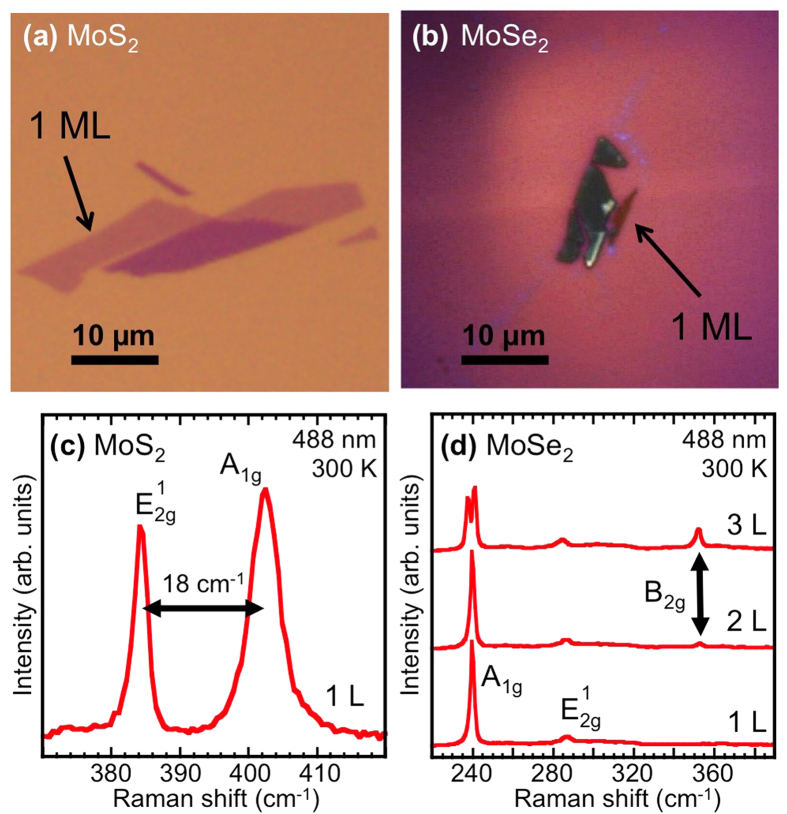
Flakes of MoS2 and MoSe2 mechanically exfoliated from bulk crystals were used in this study. Monolayer MoX2 regions were identified with an optical microscope (Fig. 2(a,b)) and confirmed with Raman spectroscopy at room temperature (Fig. 2(c,d)). Raman spectroscopy confirms single-layer regions through the shapes and relative positions of the out-of-plane A1g and in-plane E12g Raman active modes26,27,28 (see Methods section). In Fig. 2(c) the 18 cm−1 splitting between E12g (384 cm−1) and A1g (402 cm−1) modes verifies the monolayer nature of the MoS2 sample26. Raman spectra from MoSe2 taken under the same conditions are shown in Fig. 2(d) for several layer thicknesses. The identification of the single layer27 is based on the absence of the B2g mode at 353 cm−1, which can be clearly seen in Fig. 2(d). A micro-PL setup was used to collect the PL in a backscattering geometry (see methods section). The PL spectra were analyzed as σ+ and σ− using a combination of quarter-wave plate (liquid crystal retarder) and linear polarizer placed before the spectrometer entrance slit. The degree of circular polarization is defined as Pcirc = (I+ − I−)/(I+ + I−), where I+(I−) is the intensity of the σ+(σ−) component of the PL.
Figure 2. Characterization of single layers.
Optical image of (a) MoS2 and (b) MoSe2 samples. (c) Raman spectrum of single layer MoS2. The 18 cm−1 energy separation between the in-plane and out-of-plane modes is characteristic of single layer MoS2. (d) Raman spectrum of 1, 2, and 3 layers of MoSe2. Spectra are offset for clarity. The absence of the B2g mode is the fingerprint for the single layer. All spectra were taken at 300 K with an excitation wavelength of 488 nm.
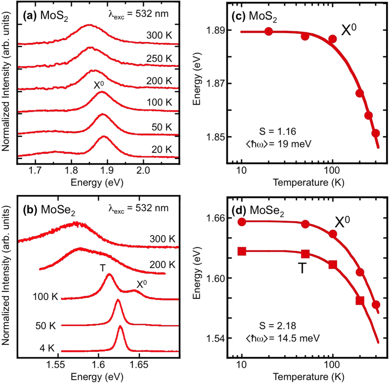
Temperature dependent PL emission from MoS2 and MoSe2 are shown in Fig. 3(a,b), respectively (full experimental details are described elsewhere)11. In these spectra, the samples were excited with a laser at 2.33 eV (532 nm). The dominant emission peak is the A-exciton, a feature that originates from the lowest energy transition at the K-point of the Brillouin zone (see Fig. 1(c)). At low temperature, we measure the A-exciton at 1.89 eV for MoS2, and at 1.625 eV for MoSe2 reflective of the smaller bandgap of MoSe2. The width of the emission from MoS2 is very broad (FWHM = 0.09 eV) so it is not possible to distinguish features within the spectra and we assign this feature to the neutral exciton, X0. However, the emission from MoSe2 is much narrower (FWHM = 0.01 eV), and it is possible to distinguish two clear peaks separated by 0.03 eV that become apparent as the sample is heated (Fig. 3(b)). These peaks have been identified as a neutral exciton (X0) and a charged exciton (T)18. It is not possible to determine whether the lower energy peak is a positive or negative charged exciton based solely on the emission energy, because the effective mass of electrons and holes in this material is similar.
Figure 3. Temperature dependence of photoluminescence.
Normalized PL spectra for (a) MoS2 and (b) MoSe2 taken with unpolarized 532 nm excitation at selected temperatures. Spectra are offset for clarity. Temperature dependent shift of the exciton emission energy in (c) MoS2 and (d) MoSe2.
As the temperature is increased the relative luminescence of charged vs. neutral exciton changes, with the neutral exciton eventually becoming the dominant feature. Note that the charged exciton is still visible at temperatures much higher than is seen in other quasi-2D systems such as GaAs QWs29. The temperature dependence of the exciton emission channels for both systems shows a typical semiconductor behavior (Fig. 3(c,d), solid symbols) and the data can be fit using a standard hyperbolic cotangent relation as defined by O’Donnell and Chen30. The solid lines are the fits to the data with the function E(T) = E(0) − S〈ħω〉[coth(〈ħω 〉/2 kT) − 1] where E(0) is the energy position of a given feature at zero temperature, S is a dimensionless coupling constant, and 〈ħω〉 is an average phonon energy. The fitting parameters obtained here are S = 1.16 (2.18) and 〈ħω〉 = 19 meV (14.5 meV) for MoS2 (MoSe2).
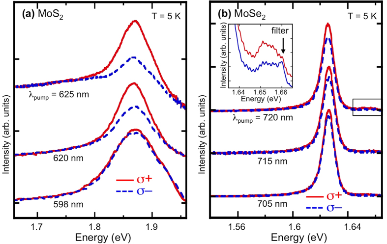
To examine the valley spin dynamics, we measure the helicity dependent PL from these monolayers. Because of the optical selection rules (Fig. 1(c)), when pumped with light of positive (σ+) or negative (σ−) helicity, either the K or K’ valley will be selectively populated6. Information on the depolarization process comes from analyzing the polarization of the subsequent PL. Figure 4(a,b) show representative PL spectra analyzed for σ+ (solid red line) and σ− (dashed blue line) at T = 5 K for MoS2 and MoSe2, respectively, at selected σ+ excitation energies. By using a combination of sharp, long-pass filters, stray light was suppressed at the spectrometer entrance. In addition, as the excitation energy approached the PL emission energy, the excited Raman modes were cut-off from entering the detection system. This experimental setup limited our lowest excitation energies to 1.984 eV (625 nm) for MoS2 and 1.722 eV (720 nm) for MoSe2. It is clear from Fig. 4 that, for both materials, the higher the excitation energy, the lower the polarization of the emission31.
Figure 4. Polarization of photoluminescence spectra.
PL spectra at T = 5 K analyzed for σ+ and σ− at selected photo-excitation energies for (a) MoS2 and (b) MoSe2. The pumping is σ+ in both cases. A dramatic decrease in the emitted circular polarization is observed as the excitation energy increases. The peaks were normalized and vertically shifted for clarity. For the MoSe2 spectra, the inset is an enlargement of the area indicated by a rectangular box and shows the neutral exciton emission.
The degree of circular polarization is shown in Fig. 5 as a function of the excess energy, ∆E = Epump − EPL, the difference between the excitation energy Eexc and PL emission energy, EPL (the inset of Fig. 5 is a graphical representation). Data are plotted for MoSe2 (solid red circles) and MoS2 (solid blue circles) and are derived from spectra where the temperature was held constant and the laser energy was varied, or the laser energy was fixed and the emission energy was varied via a change in temperature8,11,19. Since this plot incorporates the energy difference between excitation and PL emission rather than the specific energy of the neutral and charged excitons, the behavior observed for both materials can be shown. Data for MoS2 from the literature are also plotted in Fig. 5. The open circle, open square with a cross, and open triangle are data from Refs 8,10 and 20, respectively. These data were taken at 5 K with circularly polarized excitation from a HeNe laser (1.96 eV). The open squares with a slash are data from Ref 19 obtained at fixed excitation energy of 1.96 eV but at temperatures ranging from 5 to 300 K. To the best of our knowledge, these data represent the trends seen in the literature for MoS2. All data follow the same depolarization trend line when plotted as a function of excess energy. Using this methodology, all of the data collapse onto a single curve for each material, independent of whether the polarization of the trion or neutral exciton is considered. The data clearly demonstrate that as the excess energy increases the emitted circular polarization decreases.
Figure 5. Polarization dependence on excess energy.
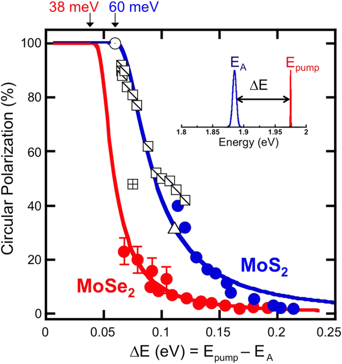
Degree of circular polarization of the emitted PL as function of excess energy, ΔΕ. Data are derived from spectra where the temperature was held constant and the laser energy was varied, or the laser energy was fixed and the emission energy was varied via a change in temperature. Solid symbols (MoSe2 is red and MoS2 is blue) are our data, and open symbols are data from references 8,10,19,20. A graphical definition of excess energy is presented in the inset. Except where noted, error bars are not in excess of the symbol size.
Discussion
To explain this behavior, we begin by noting that due to the optical selection rules6 intra-valley scattering cannot result in a reduction in the observed polarization even if the pump energy exceeds the spin-orbit splitting (160 meV for MoS2, 180 meV for MoSe2)8. Therefore, inter-valley scattering is required to account for the reduced polarization observed, and the change in momentum necessary for such scattering implicates a phonon-mediated process8,11. Close to resonance the emitted circular polarization is expected to be essentially 100%, since there is not enough energy in the system to facilitate intervalley scattering. As the laser excitation energy increases or as the temperature changes for a fixed pumping energy, the available excess energy ∆E increases and phonon-assisted scattering is enabled above some material-dependent energy threshold. For MoS2, the combined data set clearly interpolate to 100% polarization at ∆E = 60 meV, corresponding to twice the LA phonon energy11.
Intervalley scattering requires participation from in-plane longitudinal phonons. From the phonon-dispersion curves for single layers of MoS2 and MoSe2 the lowest energy phonon available for scattering are longitudinal acoustic phonons with energies of 30 meV for MoS224 and 19 meV for MoSe225. Intervalley scattering becomes accessible when the excitation energy exceeds a threshold value that is the sum of the exciton Coulombic formation energy (PL emission energy) and twice the lowest acoustic-phonon energy available in the system (essentially a phonon for each the electron and hole). That is 60 meV for MoS2 and 38 meV for MoSe2. There are two mechanisms that could be responsible for the electron or hole spin-flip during this phonon mediated intervalley scattering event. One is that the spin-flip is mediated by short range scattering from impurities. The presence of a background carrier population could enhance the probability of such a process31. The other mechanism is that intervalley scattering proceeds through the nearly spin-degenerate Γ valley of the Brillioun zone32.
The MoSe2 data (solid red symbols) exhibit a similar behavior – the measured polarization rapidly increases as the excess energy ∆E decreases. The narrow linewidths in MoSe2 allow us to distinguish the particular emission channels X0 and T. Therefore, for MoSe2, we can plot the polarization of both the neutral and charged exciton. Note that due to the low intensity of the X0 data, it is difficult to see the polarization on the same scale as the trion emission, therefore a typical set of X0 emission spectra are shown in the inset of Fig. 4(b). As with MoS2, all the data coalesce onto the same depolarization curve as a function of excess energy. The solid red line is a model fit described below, and intercepts 100% polarization at ∆E = 38 meV, corresponding to twice the MoSe2 LA phonon energy of 19 meV from the literature25. These data make it clear that depolarization and intervalley scattering are governed by the excess energy, ∆E, imparted to the photoexcited carriers through optical pumping.
To model this behavior, we begin with a familiar rate equation model in which the emitted circular polarization can be expressed as  , where τr is the exciton lifetime and τs the intervalley scattering time8,11. Both τr and τs depend on temperature, or more specifically on the thermal energy given to the exciton during optical excitation. We associate this additional thermal energy with the excess energy, ∆E. It has been shown that τr depends linearly on temperature33, therefore we expect it to have a linear dependence with ∆E. In addition, the increase in the excess energy leads to an increase of the phonon population. We assign the intervalley scattering rate τs−1 to be proportional to the phonon population
  and substitute kT with (∆E − ћωq). Taking into account these dependencies on ∆E we can fit the data using the relation
  . Here ћωq is twice the LA phonon energy, the minimum energy necessary for the exciton (electron and hole) to scatter from one valley to the other and reduce the optical polarization, and C is a scaling constant. These two values, C and ћωq, are the only fitting parameters. Note that this fitting relation is valid only for ∆E > ћωq. The solid lines in Fig. 5 are fits to the data and yield values for 2LA of 54 meV for MoS2 and 38 ± 4 meV for the MoSe2, in good agreement with the respective literature values of 60 and 38 meV24,25. The data for MoS2 diverge systematically from the fitted line above 150 meV. The main reason for this discrepancy may be that our simple rate equation model does not take into account the spin-orbit interaction (150 meV for MoS2)11.
Even though the optical response of 2-dimensional crystals is dominated by the formation of excitons, we used the phonon-assisted intervalley scattering model, which is based on a single particle picture. This is a straightforward way to describe the sharp depolarization of the emitted PL as a function of the excess energy that includes a threshold energy. However, the thermally activated relaxation of the carriers may not represent all aspects of physics that could describe the spin relaxation in this system. Recently, alternative interpretations based on the excitonic picture explain the PL depolarization as valley-decoherence due to long-range exciton exchange, i.e. direct intervalley electron-hole exchange32,34,35,36,37,38. Both of these mechanisms may be at play with different relative contributions that varies across different material systems. Our observation of a threshold depolarization energy, however, is more easily explained with the phonon model we have presented.
In summary, at zero magnetic field, we initialized circular polarization in MoS2 and MoSe2 using energy-dependent circularly-polarized optical pumping and measured the valley polarization process as a function of the excess energy absorbed by the carriers. Independent of the emission channel or the material studied (MoS2 or MoSe2), all the data can be modeled by a single depolarization mechanism, intervalley scattering mediated by LA phonons. The threshold needed for depolarization is found to be twice the LA phonon energy of the corresponding material, and the exciton kinetic energy greater than this is the key parameter for the depolarization. Generating high chirality photoluminescence in Mo-based two-dimensional structures enables applications in valley-photonics.
Methods
Sample preparation and characterization
All samples used in this study were mechanically exfoliated from bulk crystals. The MoS2 was deposited onto a 285-nm SiO2 layer on a Si substrate, while the MoSe2 flakes were deposited on a 90-nm SiO2 layer on a Si substrate. The typical size of monolayer regions are 5–10 μm across for MoS2 and 1–2 μm for MoSe2 and were identified with an optical microscope and confirmed with Raman spectroscopy at room temperature and 488 nm excitation. Raman spectroscopy has been established as a reliable tool for determining the specific number of layers in transition metal dichalcogenides26,27,28. In MoS2, the 18 cm−1 energy difference between the two main vibrational modes, E12g at 384 cm−1 and A1g at 402 cm−1, is the fingerprint for the accurate determination of the single layer. In MoSe2, the in-plane E12g (287 cm−1) and the out-of-plane A1g (242 cm−1) modes are much lower in energy than in MoS2 because of the larger mass of the Se atom. Also, the in-plane and out-of-plane modes switch positions relative to the MoS2, i.e, the out-of-plane mode is softer than the in-plane one. This can be verified by measuring thicker layers of MoSe2 and observing a Davydov splitting in the A1g mode for multi-layer flakes. The single layer is identified by the absence of the B2g mode at 353 cm−1.
Optical measurements
The photoluminescence data were taken in a backscattering geometry using a micro-PL setup (spatial resolution of 1 μm) with a 50× objective and incorporating a continuous-flow He-cryostat. The MoS2 samples were excited with either a continuous-wave 2.33 eV (532 nm) solid-state laser or a tunable pulsed laser while the MoSe2 flakes were excited by a continuous-wave Ti:Sapphire laser. The pulsed source was an optical parametric amplifier (pumped by a Ti:Sapphire laser) tunable from 1.77–2.48 eV (700–500 nm) at a 250-kHz repetition rate with a double-pass grating (500 g/mm) geometry to reduce the spectral bandwidth to <5 meV (1 nm). The photoluminescence emission was collected, passed though a polarization analyzer, and dispersed by a single monochromator equipped with a multichannel charge coupled device (CCD) detector.
Additional Information
How to cite this article: Kioseoglou, G. et al. Optical polarization and intervalley scattering in single layers of MoS2 and MoSe2. Sci. Rep. 6, 25041; doi: 10.1038/srep25041 (2016).
Acknowledgments
We would like to thank Jim Culbertson for assistance with Raman measurements. G.K. gratefully acknowledges the hospitality and support of the Naval Research Laboratory where the experiments were performed. This work was supported by core programs at NRL and the NRL Nanoscience Institute, and by Air Force Office of Scientific Research under contract number F4GGA24233G001.
Footnotes
Author Contributions G.K., A.H. and M.C. performed the experiments. G.K., A.H. and M.C. analyzed the data. A.F. fabricated the samples. All authors discussed the results and A.H., G.K., M.C. and B.J. wrote the manuscript.
References
- Mak K. F., Lee C., Hone J., Shan J. & Heinz T. F. Atomically Thin MoS2: A New Direct-Gap Semiconductor. Phys. Rev. Lett. 105, 136805 (2010). [DOI] [PubMed] [Google Scholar]
- Splendiani A. et al. Emerging Photoluminescence in Monolayer MoS2. Nano Lett. 10, 1271–1275 (2010). [DOI] [PubMed] [Google Scholar]
- Korn T., Heydrich S., Hirmer M., Schmutzler J. & Schüller C. Low-temperature photocarrier dynamics in monolayer MoS2. Appl. Phys. Lett. 99, 102109 (2011). [Google Scholar]
- Bernardi M., Palummo M. & Grossman J. C. Extraordinary Sunlight Absorption and One Nanometer Thick Photovoltaics Using Two-Dimensional Monolayer Materials. Nano Letters 13, 3664–3670 (2013). [DOI] [PubMed] [Google Scholar]
- Perkins F. K. et al. Chemical Vapor Sensing with Monolayer MoS2. Nano Letters 13, 668–673 (2013). [DOI] [PubMed] [Google Scholar]
- Xiao D., Liu G.-B., Feng W., Xu X. & Yao W. Coupled Spin and Valley Physics in Monolayers of MoS2 and Other Group-VI Dichalcogenides. Phys. Rev. Lett. 108, 196802 (2012). [DOI] [PubMed] [Google Scholar]
- Zhu Z. Y., Cheng Y. C. & Schwingenschlögl U. Giant spin-orbit-induced spin splitting in two-dimensional transition-metal dichalcogenide semiconductor. Phys. Rev. B 84, 153402 (2011). [Google Scholar]
- Mak K. F., He K., Shan J. & Heinz T. F. Control of valley polarization in monolayer MoS2 by optical helicity. Nat. Nanotechnol. 7, 494–498 (2012). [DOI] [PubMed] [Google Scholar]
- Mak K. F. et al. Tightly bound trions in monolayer MoS2. Nat. Mater. 12, 207–211 (2012). [DOI] [PubMed] [Google Scholar]
- Cao T. et al. Valley-selective circular dichroism of monolayer molybdenum disulphide. Nat. Commun. 3, 887 (2012). [DOI] [PMC free article] [PubMed] [Google Scholar]
- Kioseoglou G. et al. Valley polarization and intervalley scattering in monolayer MoS2. Appl. Phys. Lett. 101, 221907 (2012). [Google Scholar]
- Davelou D., Kopidakis G., Kioseoglou G. & Remediakis I. N. MoS2 nanostructures: Semiconductors with metallic edges. Solid State Comm. 192, 42–46 (2014). [Google Scholar]
- Qiu D. Y., da Jornada F. H. & Louie S. G. Optical Spectrum of MoS2: Many-Body Effects and Diversity of Exciton States. Phys. Rev. Lett. 111, 216805 (2013). [DOI] [PubMed] [Google Scholar]
- Hanbicki A. T., Currie M., Kioseoglou G., Friedman A. L. & Jonker B. T. Measurement of high exciton binding energy in the monolayer transition-metal dichalcogenides WS2 and WSe2. Solid State Commun. 203, 16–20 (2015). [Google Scholar]
- Ramasubramaniam A. Large excitonic effects in monolayers of molybdenum and tungsten dichalcogenides. Phys. Rev. B 86, 115409 (2012). [Google Scholar]
- He K. et al. Tightly Bound Excitons in Monolayer WSe2. Phys. Rev. Lett. 113, 026803 (2014). [DOI] [PubMed] [Google Scholar]
- Chernikov A. et al. Exciton Binding Energy and Nonhydrogenic Rydberg Series in Monolayer WS2. Phys. Rev. Lett. 113, 076802 (2014). [DOI] [PubMed] [Google Scholar]
- Ross J. S. et al. Electrical control of neutral and charged excitons in a monolayer semiconductor. Nature Communications 4, 1474 (2013). [DOI] [PubMed] [Google Scholar]
- Sallen G. et al. Robust optical emission polarization in MoS2 monolayers through selective valley excitation. Phys. Rev. B 86, 081301R (2012). [Google Scholar]
- Zeng H., Dai J., Yao W., Xiao D. & Cui X. Valley polarization in MoS2 monolayers by optical pumping. Nat. Nanotechnol. 7, 490–493 (2012). [DOI] [PubMed] [Google Scholar]
- Wang G. et al. Polarization and time-resolved photoluminescence spectroscopy of excitons in MoSe2 monolayers. Appl. Phys. Lett. 106, 112101 (2015). [Google Scholar]
- MacNeil D. et al. Breaking of Valley Degeneracy by Magnetic Field in Monolayer MoSe2. Phys. Rev. Lett. 114, 037401 (2015). [DOI] [PubMed] [Google Scholar]
- Li Y. et al. Valley Splitting and Polarization by the Zeeman Effect in Monolayer MoSe2. Phys. Rev. Lett. 113, 266804 (2014). [DOI] [PubMed] [Google Scholar]
- Molina-Sánchez A. & Wirtz L. Phonons in single-layer and few-layer MoS2 and WS2. Physical Review B 84, 155413 (2011). [Google Scholar]
- Horzum S. et al. Phonon Softening and direct to indirect band gap crossover in strained single-layer MoSe2. Phys. Rev. B 87, 125415 (2013). [Google Scholar]
- Lee C. et al. Anomalous Lattice Vibrations of Single-and Few-Layer MoS2. ACS Nano 4, 2695–2700 (2010). [DOI] [PubMed] [Google Scholar]
- Tonndorf P. Photoluminescence emission and Raman response of monolayer MoS2, MoSe2, and WSe2. Optics Express 21, 4908–4916 (2013). [DOI] [PubMed] [Google Scholar]
- Tongay S. et al. Thermally Driven Crossover from Indirect toward Direct Bandgap in 2D Semiconductors: MoSe2 versus MoS2. Nano Lett. 12, 5576–5580 (2012). [DOI] [PubMed] [Google Scholar]
- Kioseoglou G. et al. Photoluminescence and reflectance studies of negatively charged excitons in GaAs/AlGaAs quantum-well structres. Phys. Rev. B 61, 4780 (2000). [Google Scholar]
- O’Donnell K. P. & Chen X. Temperature dependence of semiconductor band gaps. Appl. Phys. Lett. 58, 2924 (1991). [Google Scholar]
- Song Y. & Dery H. Transport Theory of Monolayer Transition-Metal Dichalcogenides through Symmetry. Phys. Rev. Lett. 111, 026601 (2013). [DOI] [PubMed] [Google Scholar]
- Mai C. et al. Many-Body Effects in Valleytronics: Direct Measurement of Valley Lifetimes in Single-Layer MoS2. Nano Lett. 14, 202–206 (2014). [DOI] [PubMed] [Google Scholar]
- Palummo M., Bernardi M. & Grossman J. C. Exciton Radiative Lifetimes in Two-Dimensional Transition Metal Dichalcogenides. Nano Lett. 15, 2794–2800 (2015). [DOI] [PubMed] [Google Scholar]
- Glazov M. M. et al. Exciton fine structure and spin decoherence in monolayers of transition metal dichalcogenides. Phys. Rev. B 89, 201302 (2014). [Google Scholar]
- Yu T. & Wu M. W. Valley depolarization due to intervalley and intravalley electron-hole exchange interactions in monolayer MoS2. Phys. Rev. B 89, 205303 (2014). [Google Scholar]
- Dery H. & Song Y. Polarization analysis of excitons in monolayer and bilayer transition-metal dichalcogenides. Phys. Rev. B 92, 125431 (2015). [Google Scholar]
- Glazov M. M. et al. Spin and valley dynamics of excitons in transition metal dichalcogenide monolayers. Phys. Status Solidi B 252, 2349–2362 (2015). [Google Scholar]
- Dal Conte S. et al. Ultrafast valley relaxation dynamics in monolayer MoS2 probed by nonequilibrium optical techniques. Phys. Rev. B 92, 235425 (2015). [Google Scholar]


