Researchers detect individual CO2 physisorption with suspended bilayer graphene based on induced Coulomb impurity scattering.
Keywords: graphene, Physisorption, Coulomb Impurity Scattering, Gas Sensing
Abstract
Detection of individual molecular adsorption, which represents the ultimate resolution of gas sensing, has rarely been realized with solid-state devices. So far, only a few studies have reported detection of individual adsorption by measuring the variation of electronic transport stemming from the charge transfer of adsorbate. We report room-temperature detection of the individual physisorption of carbon dioxide molecules with suspended bilayer graphene (BLG) based on a different mechanism. An electric field introduced by applying back-gate voltage is used to effectively enhance the adsorption rate. A unique device architecture is designed to induce tensile strain in the BLG to prevent its mechanical deflection onto the substrate by electrostatic force. Despite the negligible charge transfer from a single physisorbed molecule, it strongly affects the electronic transport in suspended BLG by inducing charged impurity, which can shut down part of the conduction of the BLG with Coulomb impurity scattering. Accordingly, we can detect each individual physisorption as a step-like resistance change with a quantized value in the BLG. We use density functional theory simulation to theoretically estimate the possible resistance response caused by Coulomb scattering of one adsorbed CO2 molecule, which is in agreement with our measurement.
INTRODUCTION
Solid-state gas sensors, which have been widely used to detect oxygen depletion and combustible, flammable, and toxic gases, are of great interest for industrial, environmental, and military monitoring (1). Sensing is based mainly on the electrical conductivity change in a material upon the adsorption of gas molecules. A variety of materials, such as inorganic semiconductors (2), conjugated polymers (3), and nanomaterials (4), have been explored. Graphene, a two-dimensional (2D) form of pure carbon, has recently been drawing much attention as a promising candidate for gas sensing because of its ultralow thickness and excellent electronic properties (5). Graphene has the largest sensing area per unit volume of any solid material. All atoms in a monolayer or bilayer graphene (BLG) are considered surface atoms, and they are able to adsorb gas molecules. Moreover, owing to its high-quality crystal lattice, along with its 2D structure, graphene exhibits extremely suppressed electrical noise (6), making it possible to measure weak fluctuations in its transport properties.
Several studies on high-resolution sensing of gases with graphene at ~10 parts per million have been published (7, 8). However, reaching the ultimate resolution (that is, detecting an individual adsorption event) remains challenging. So far, only one study, conducted by Schedin et al. (9), has used graphene to detect an individual adsorption event. In their experiment, the charge transfer between adsorbed nitrogen dioxide molecules and graphene in an individual adsorption event varied the carrier density in the graphene, which was measured as quantized Hall conductance changes under an ultrahigh magnetic field of 10 T. Besides carrier density variation, the degraded carrier mobility should be measured because of adsorption-induced Coulomb impurity scattering. Practically, reduced mobility upon exposure to a gas environment has not been observed in graphene in many experiments (9–11). Considering that conventional SiO2 supported graphene, massively charged impurities from a defective substrate effectively screen off any surface-charged impurities (12, 13). Moreover, the dielectric mismatch between substrate and graphene also suppresses impurity-induced Coulomb potential and therefore weakens the scattering (14). In general, surface adsorption–induced Coulomb impurity scattering insignificantly affects electronic transport in graphene.
Here, we report room-temperature electrical detection of an individual CO2 physisorption event using freely suspended BLG. We designed a special device architecture to induce tensile strain in the graphene to maintain its suspension even at considerable back-gate voltage. It allows us to introduce an electric field on the graphene surface to accelerate the molecular adsorption process in a low-concentration CO2 environment. By eliminating the screening of substrate-charged impurities and dielectric mismatch, adsorption-induced Coulomb impurity scattering in suspended graphene can lead to significant changes in transport behavior. As a result, the step-like resistance change (~61 ohms) is measured in the graphene at each individual physisorption. A quantitative estimation using density functional theory (DFT) simulation suggests that an increment of ~50 ohms in graphene with one adsorbed CO2 molecule is essentially in agreement with our measurement.
RESULTS AND DISCUSSIONS
We started with a BLG double-clamped on electrodes (Ti/Au) and suspended over a bottom electrode to detect physisorption (Fig. 1A, also see fig. S1 and Materials and Methods) (15). Thereafter, graphene was electrostatically pulled onto the bottom electrode by applying a 2.7-V voltage between the top and bottom electrodes (fig. S2 and Materials and Methods). Structurally, the final device consists of the bottom electrode, one top electrode, and the segment of graphene between them. Figure 1 (B and C) displays its topography and height profile, obtained by tapping-mode atomic force microscopy. We clearly note an ~300-nm-long, ~1.1-μm-wide graphene suspended over the SiO2 substrate between the top electrode and the bottom electrode.
Fig. 1. Suspended strained graphene device.
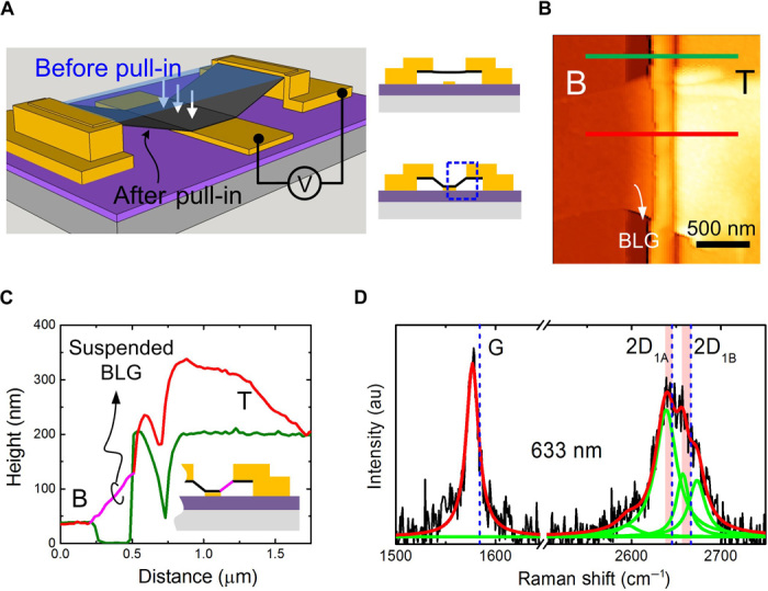
(A) Schematic of pulling a suspended graphene with electrostatic force onto the bottom electrode. Right panels are the side views before and after pull-in. The blue dashed box highlights the suspended graphene used for adsorption detection. (B) Atomic force microscopy image of the suspended BLG device [marked by the blue dashed box in (A)]. B, bottom; T, top. (C) Height profiles along the green and red lines in (B). The pink line highlights the suspended BLG. (D) Raman spectrum of the suspended graphene. The green lines are the Lorentzian subpeaks fitted to the 2D band. The blue dotted lines locate the G, 2D1A, and 2D1B bands of a pristine BLG, respectively. Red shadows mark stain-induced shifts in the 2D band. au, arbitrary units.
Figure 1D shows the Raman spectrum measured on the suspended graphene. Four Lorentzian subpeaks can be fitted to the 2D band, showing the clear BLG signature (16, 17). Furthermore, owing to geometric deformation (uniaxial tensile strain is built in the suspended BLG), these subpeaks are identified with obvious red shifts compared with those of a pristine BLG (16). Accordingly, a considerable tensile strain of ~0.44% is estimated (see Materials and Methods for the detailed analysis). Benefiting from this, graphene can maintain suspension even at a high back-gate voltage Vg of 30 V, whereas its band structure topology remains mostly unchanged (18).
The gate modulation measurement of the fabricated device (see Materials and Methods for the details) exhibits clear ambipolar characteristics with a weakly shifted charge neutral point (CNP) at −5 V and negligible hysteresis (Fig. 2A), suggesting unstained graphene. The slight n-type doping possibly stems from the metal at the electrical contacts. For instance, gold on the bottom contact, which has a work function of 5.54 eV [very close to the crossover work function of graphene (5.4 eV)], weakly dopes graphene as an acceptor (19). Titanium on the top contact has a much lower work function of 4.33 eV, doping graphene strongly as a donor. Generally speaking, n-type doping dominates.
Fig. 2. Measurements of CO2 detection with the suspended BLG.
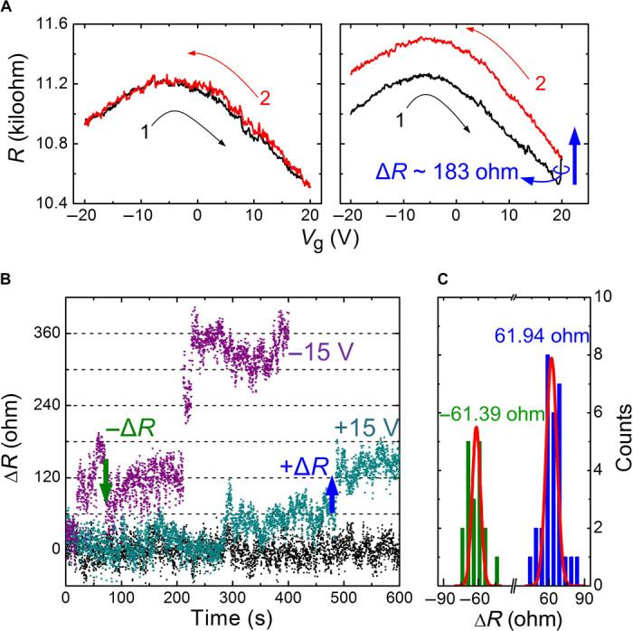
(A) Gate modulations in a vacuum (left) and in a CO2 environment (right). (B) Resistance responses of BLG exposed to CO2 with Vg of 0 V (black dots), +15 V, and −15 V, respectively. The blue and green arrows highlight the positive and negative step-like changes in resistance, respectively. (C) Statistical distribution of the step-like change in resistance ΔR in BLG exposed to CO2 with a Vg of +15 V. The solid lines are Gaussian fits.
We monitored the resistance of graphene exposed to a pure CO2 environment of a low concentration of 0.73 molecules/μm3 at room temperature to detect the signal from adsorption (see Materials and Methods). The low concentration ensures slow molecular adsorption on graphene, with a long-enough interval between two events to distinguish the signal from one of them. However, if the adsorption rate is too low, there is probably no adsorption occurring in the measured span. A nearly constant resistance accompanied by random noise, which probably originated from the strain and thermal fluctuations in the BLG, was observed over a 10-min period (black dots in Fig. 2B). The molecular adsorption can be accelerated by introducing an external electric field on the graphene surface, with back-gate voltage applied to the substrate. We measured a pronounced resistance change in a 10-min period with a Vg of 15 V (Fig. 2B); note the step-like feature. We infer that the signal originates from discrete events (that is, individual adsorption). We performed statistical analysis on the resistance increments, considering only abrupt resistance changes. Slow and weak changes were ignored as noise. The resulting histogram in Fig. 2C apparently exhibits two quantized values of +61.9 and −61.4 ohms (relative change of approximately ±0.6%; see fig. S3), corresponding to the detection of individual CO2 adsorption and desorption events, respectively. In addition, the device is easily regenerated by a short current annealing, and the measurement is repeatable (see fig. S4). It highlights the physisorptive nature of the adsorptive occurring on the graphene.
Mechanism of electric field–accelerated physisorption
Despite the lack of polarization, charge distribution in CO2 molecules can be distorted from the normal shape by an electric field (20). For instance, the application of Vg = 15 V generates an electric field E of ~106 V/m on the graphene surface, leading to a dipole moment P of 2.79 × 10⁻³⁴ C·m in the polarized CO2 molecule (see Materials and Methods). These molecules, having their electric dipoles oriented parallel to the electric field, are attracted toward regions where field intensity is high (for example, the graphene surface). A semiempirical electrostatic simulation illustrates a strong electrostatic potential zone enveloping the graphene surface (Fig. 3A). Molecules must climb a potential hill as they move into a high field region on the graphene surface and lose kinetic energy. Consequently, they are easier to capture by graphene via van der Waals (vdW) interactions. The trajectories of one molecule traveling toward the graphene surface are visualized by the molecular dynamics simulations (see Materials and Methods and the Supplementary Materials). In the absence of an electric field, the molecule bounces off the graphene surface and escapes easily from surface interaction by considering its relatively high kinetic energy at 300 K (Fig. 3B). In contrast, when applying an electric field, the bounced molecule finds it hard to break loose from vdW bonding as a result of the reduced kinetic energy; therefore, it is easily adsorbed onto the graphene (Fig. 3C).
Fig. 3. Molecular dynamics simulations of CO2 motion over a graphene surface in an electric field.
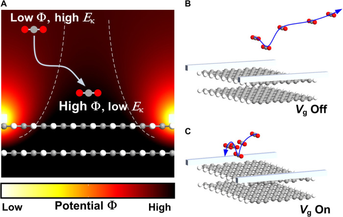
(A) Potential distribution on the graphene surface with the application of back-gate voltage. The area with high potential is located between the two dashed lines. (B and C) Molecular dynamics simulations of the trajectory of a free CO2 molecule near the graphene surface at 300 K from 0 to 4 ps without (B) and with (C) Vg. The arrow lines give the trajectory of the molecule.
Origin of resistance change caused by physisorption
The conductivity σ of a conducting material is expressed as σ = nμe, where n, μ, and e are the carrier density, mobility, and electron charge, respectively. Thus, any resistance variation can be attributed to either the change in n or the change in μ. In most previous reports, charge transfer between surface adsorbates and graphene is responsible for the resistance change in graphene by varying n (9).
Supposing that charge transfer from CO2 molecules dominates transport in the graphene, the doping effect must shift the CNP to the positive voltage side. It is then reasonable to expect the opposite signs for resistance changes measured at the gate voltages lower and higher than the CNP, as sketched in Fig. 4A. However, the positive resistance increment ΔR of ~60 ohms is again measured at Vg = −15 V, indicating a different determining factor other than charge transfer. In addition to charge transfer, the charged impurity induced by adsorption strengthens the scattering in the graphene, which reduces the carrier mobility μ and increases resistance. When it dominates the transport, a shifted gate modulation curve to higher resistance is measured after adsorption, with negligible CNP shifting (Fig. 4B). This is consistent with our measurement shown in Fig. 2A (also see an additional measurement in fig. S5). The gate modulation was investigated with a regenerated device. An abrupt change of ~183 ohms occurs at Vg = 19 V during gate voltage sweeping, which can be ascribed to three simultaneous physisorption events. After adsorption, a gate modulation curve with a shape and a CNP value identical to those observed before adsorption is measured with a clear resistance increment of ~180 ohms. We are thus confident in arguing that any resistance changes measured by exposure to molecules should find their origin in adsorption-induced impurity scattering.
Fig. 4. Schematics of the gate modulations of graphene before and after molecular physisorption.
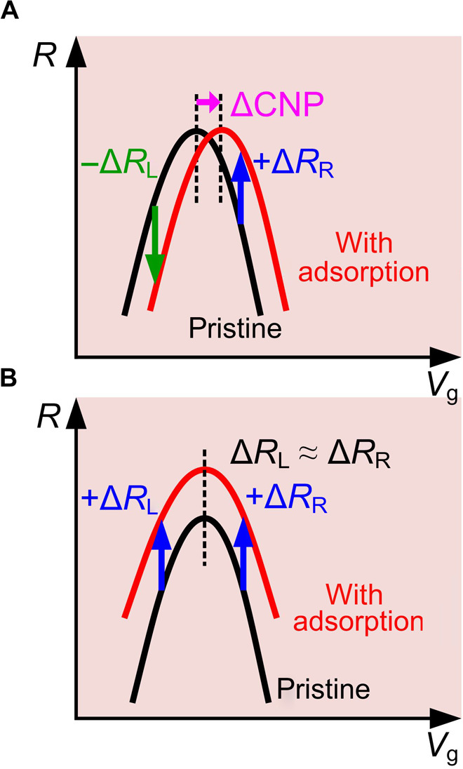
(A) When charge transfer dominates. (B) When impurity scattering dominates.
To verify the likelihood of the scenario, we carried out DFT calculations with vdW correction to simulate the charged impurity distribution in graphene caused by CO2 adsorption (Materials and Methods; see more detailed information in the Supplementary Materials) (21).
First, we highlight the advantages of using suspended graphene to detect surface adsorption. Figure 5A displays the cross-sectional charge density difference distributions along a CO2 adsorbate in a freestanding (suspended) BLG. CO2 molecules cause a strong localization of electron density depletion (that is, positively charged impurity) in an upper basal plane expanded around the adsorption site. It is not completely screened by graphene; although reduced, the lower plane remains affected, exhibiting a less-expanded charged impurity distribution. In terms of graphene placed on an SiO2 substrate, we need to take account of the charged impurities originating from the inevitable defects residing on the substrate surface. The simulation shows the excessive impurities distributing all over the graphene without distinct localization (Fig. 5B). Such serious doping, as well as significant charge density inhomogeneity, has been experimentally demonstrated in graphene supported on an SiO2 substrate using scanning tunneling microscopy (22). The screening of substrate impurities can strongly reduce the impurity potential of the surface adsorbate (12). Similarly, if any predefined impurities (for example, organic residues) exist on the BLG surface, they are also responsible for screening off the Coulomb potential of the molecules adsorbed in the neighboring area. Even with a defectless SiO2 substrate, the distribution of localized impurity is suppressed; especially in the lower basal plane, we note barely any local impurity (Fig. 5C). Moreover, BLG in an electric field is an atomically thin semiconductor, where the carrier-charged impurity Coulomb interaction highly depends on the surrounding dielectric environment (14). In the suspended BLG, the impurity Coulomb interaction can be strongly enhanced by the low dielectric constant (=1). In conclusion, the electronic transport in the suspended BLG is more sensitive to the presence of surface adsorption compared with the conventionally supported BLG.
Fig. 5. Transport properties in the BLG affected by surface CO2 physisorption.
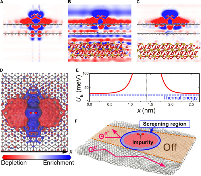
(A to C) Cross-sectional charge density difference distribution along the CO2 molecule: in freestanding BLG, in BLG placed on a defective SiO2 surface, and in BLG placed on an ideal SiO2 surface, respectively. (D) Top view of the simulated charge density difference distribution in freestanding BLG with one CO2 adsorption event. Blue and red denote electron density enrichment and depletion with an isovalue of 6 × 10⁻⁶ e/Å3 in all simulations, respectively. (E) Coulomb potential energy distribution on the x axis on the BLG along a CO2 molecule. The blue dashed line indicates the thermal energy at room temperature. The thin dotted line marks the location of a CO2 molecule. (F) Schematic of partial conducting channel shutoff in BLG by Coulomb impurity scattering.
Finally, we attempt to infer the possible resistance increment of graphene caused by an individual CO2 physisorption event. Figure 5D exhibits the charged impurity spreads in the BLG from the adsorption site to an ~2.7-nm-wide region (also see fig. S6). It produces a Coulomb potential envelope in the BLG with energy higher than thermal energy at room temperature, which is strong enough to completely block carrier diffusion (Fig. 5E). In addition, we calculate the carrier-charged impurity Coulomb screening length Ls = 1.2 nm in the suspended BLG by applying the Thomas-Fermi theory Ls = (κћ2)/(gsgvme2) (23), where κ is the background dielectric constant, ћ is the Dirac constant, gsgv is the degeneracy factor, and m is the electron mass. In total, the conduction of an ~5.1-nm-wide channel in a 1.1-μm-wide BLG is completely switched off because of one physisorbed CO2 molecule. The resulting resistance increment of ~50 ohms is in agreement with our measurement.
We detected the individual physisorption event of CO2 molecules as a step-like resistance response in the suspended BLG at room temperature. Unlike the widely investigated charge transfer, Coulomb scattering of charged impurities induced by adsorbed molecules is the determining factor of crucial change in electronic transport. As an electronically quite solid material, graphene is promising for realizing ultrasensitive sensors for active small-molecule gases. Moreover, our results entice us to investigate the possibility of using suspended graphene as a platform to study intermolecular interactions in the surface adsorption phenomena.
MATERIALS AND METHODS
Device fabrication and characterization
We prepared a double-clamped graphene suspended over a local bottom electrode, followed by the previously developed etching-free process (15): (i) define the bottom electrode (Ti/Au stack) on a 300-nm-thick SiO2/p-silicon substrate; (ii) spin-coat a polymethyl methacrylate (PMMA) polymer on the substrate; (iii) mechanically exfoliate BLG on the PMMA layer over the bottom electrode; (iv) define top contacts (Ti/Au stack) to BLG via electron beam lithography with methyl methacrylate 8.5 methacrylic acid/PMMA bilayer resist; and (v) dissolve polymers to release graphene and dry the sample in a critical point drier. Figure S1 illustrates the fabricated device. Then, graphene was electrostatically deflected onto the bottom electrode, with a voltage applied between the top electrode and the bottom electrode, as shown in Fig. 1A. Figure S2 shows the pull-in of graphene onto the bottom electrode at 2.7 V, where an abrupt increase in current was observed. Raman spectroscopy with 633-nm laser excitation was measured on the suspended graphene (Fig. 1D), allowing information on the uniaxial strain Îμ in graphene to be extracted. It is roughly correlated to the Raman frequency of the 2D band by ε = Δω/(ω0γ(1 − ν)) (24), where γ (=1.99) is the Grüneisen parameter, ν (=1.3) is the Poisson ratio of freestanding graphene (25), and Δω/ω0 (≈2.7%) is the relative shift of the 2D band due to strain. 2D1A and 2D1B peaks (two primary subpeaks in the 2D band) were identified at 2639.6 and 2657.1 cm–1, respectively, showing obvious red shifts compared with those of a pristine BLG at 2644 and 2667 cm–1 (16). Accordingly, a considerable tensile strain of ~0.44% was estimated. Before measurement, current annealing was carried out to improve electrical contact and to remove contamination from the graphene surface (26). Then, the ohmic electrical contact was confirmed by the linear current-voltage response. Gate modulation of the annealed graphene was conducted in a vacuum of ~10–5 Pa, with a silicon substrate acting as back-gate.
Electrical measurement of CO2 molecular adsorption
Electrical measurements were carried out in low-pressure pure CO2 gas at room temperature using an Agilent B1500A semiconductor analyzer. The low-pressure CO2 environment was prepared as follows: We first evacuated the chamber to a high vacuum at 10−5 Pa with a turbo molecular pump and then vented it with pure CO2 gas. The procedure was repeated three times. Finally, the chamber filled with CO2 gas was carefully pumped down to 3 × 10⁻³ Pa. Using the ideal gas model, the concentration of CO2 molecules is calculated as 0.73 molecules/μm3 (in other words, ~280 parts per billion, assuming atmospheric pressure with carrier gas injected). Before each measurement, current annealing was unitized to regenerate the graphene. In resistance measurements, the suspended BLG was constantly biased at 5 mV. The application of back-gate voltage was utilized to polarize CO2 molecules near the BLG surface by generating an electric field E. The dipole moment P is roughly estimated by P = 4πε0αE (20), where ε0 is the vacuum permittivity and α (=2.507 Å3) is the polarizability of CO2 (27).
Molecular dynamics simulations
We performed Slator-Koster semiempirical molecular dynamics simulations under Neumann boundary conditions using an Atomistix ToolKit (version 2014.3) (28). The model is presented in fig. S7. Different potentials were applied to the top electrode, bottom electrode, and back-gate. Tight coupling of temperature is necessary to effectively reproduce the kinetic energy of molecules. Therefore, we carried out an NVT (constant number of particles, volume, and temperature) ensemble molecular dynamics simulation with a Langevin thermostat at 300 K. In this simulation, the BLG was fixed in position.
DFT simulations
First, geometric optimization for the configuration of CO2 adsorbed on BLG was obtained using the SIESTA package, with implementation of vdW density functionals (29–31). Norm-conserving pseudo-potentials of Troullier and Martins were used. The integration grids in real space had a maximum kinetic energy cutoff of 400 Ry. Double-ζ plus polarization basis sets were applied in these calculations. The configurations of BLG-CO2 molecules were optimized by fully relaxing the atomic structures until the remaining residual force was lower than 0.01 eV/Å. The final configuration provides accurate values (for example, distance and orientation of the CO2 molecule) for plotting the charge density difference. To do this, we used the CASTEP package with an ultrasoft pseudo-potential, plane-wave basis, and periodic boundary conditions (25). The generalized gradient approximation with Perdew-Burke-Ernzerhof functional and a plane-wave basis set cutoff energy of 340 eV were used in the single-point energy calculation with a semiempirical Grimme dispersion correction scheme. The charge density difference in CO2 adsorption is defined as , where , , and are the charge densities of graphene (+SiO2 substrate) with adsorbed CO2, pristine graphene (+SiO2 substrate), and isolated CO2 molecule, respectively. We set the energy convergence to 1 × 10⁻⁶ eV/atom to produce a calculation with fine resolution.
Supplementary Material
Acknowledgments
We thank X. Wang for fruitful discussions. Funding: This work was supported by a Grant-in-Aid for Scientific Research (number 25220904) from the Japan Society for the Promotion of Science. Author contributions: J.S. and H.M. conceived the project. J.S. performed the experiments, analyzed the data, and wrote the manuscript. M.M. conducted molecular dynamics simulations and DFT calculations. All authors discussed the results and commented on the manuscript. Competing interests: The authors declare that they have no competing interests. Data and materials availability: All data needed to evaluate the conclusions in the paper are present in the paper and/or the Supplementary Materials. Additional data related to this paper may be requested from the authors.
SUPPLEMENTARY MATERIALS
Supplementary material for this article is available at http://advances.sciencemag.org/cgi/content/full/2/4/e1501518/DC1
fig. S1. Optical microscopic image of the as-fabricated double-clamped BLG device.
fig. S2. Measurement showing BLG pulled into the bottom electrode.
fig. S3. Relative changes in the resistance response of BLG plotted in Fig. 2B.
fig. S4. Additional measurements of the resistance time revolution of current annealing regenerated the suspended BLG.
fig. S5. Gate modulation of an additional suspended BLG in a CO2 environment.
fig. S6. Simulated charge density difference distribution in freestanding BLG, with one CO2 adsorption event occurring in a large supercell.
fig. S7. Model used in semiempirical molecular dynamics simulations.
DFT calculations with vdW correction.
REFERENCES AND NOTES
- 1.Wagner T., Haffer S., Weinberger C., Klaus D., Tiemann M., Mesoporous materials as gas sensors. Chem. Soc. Rev. 42, 4036–4053 (2013). [DOI] [PubMed] [Google Scholar]
- 2.Tricoli A., Righettoni M., Teleki A., Semiconductor gas sensors: Dry synthesis and application. Angew. Chem. Int. Ed. Engl. 49, 7632–7659 (2010). [DOI] [PubMed] [Google Scholar]
- 3.Kreno L. E., Leong K., Farha O. K., Allendorf M., Van Duyne R. P., Hupp J. T., Metal–organic framework materials as chemical sensors. Chem. Rev. 112, 1105–1125 (2012). [DOI] [PubMed] [Google Scholar]
- 4.Sharma S., Madou M., A new approach to gas sensing with nanotechnology. Philos. Trans. A Math. Phys. Eng. Sci. 370, 2448–2473 (2012). [DOI] [PubMed] [Google Scholar]
- 5.Yavari F., Koratkar N., Graphene-based chemical sensors. J. Phys. Chem. Lett. 3, 1746–1753 (2012). [DOI] [PubMed] [Google Scholar]
- 6.Lin Y.-M., Avouris P., Strong suppression of electrical noise in bilayer graphene nanodevices. Nano Lett. 8, 2119–2125 (2008). [DOI] [PubMed] [Google Scholar]
- 7.Yoon H. J., Jun D. H., Yang J. H., Zhou Z., Yang S. S., Cheng M. M.-C., Carbon dioxide gas sensor using a graphene sheet. Sens. Actuators B Chem. 157, 310–313 (2011). [Google Scholar]
- 8.Yavari F., Chen Z., Thomas A. V., Ren W., Cheng H.-M., Koratkar N., High sensitivity gas detection using a macroscopic three-dimensional graphene foam network. Sci. Rep. 1, 116 (2011). [DOI] [PMC free article] [PubMed] [Google Scholar]
- 9.Schedin F., Geim A. K., Morozov S. V., Hill E. W., Blake P., Katsnelson M. I., Novoselov K. S., Detection of individual gas molecules adsorbed on graphene. Nat. Mater. 6, 652–655 (2007). [DOI] [PubMed] [Google Scholar]
- 10.Chen G., Paronyan T. M., Harutyunyan A. R., Sub-ppt gas detection with pristine graphene. Appl. Phys. Lett. 101 053119 (2012). [Google Scholar]
- 11.Dan Y., Lu Y., Kybert N. J., Luo Z., Johnson A. T., Intrinsic response of graphene vapor sensors. Nano Lett. 9, 1472–1475 (2009). [DOI] [PubMed] [Google Scholar]
- 12.Liang S.-Z., Chen G., Harutyunyan A. R., Sofo J. O., Screening of charged impurities as a possible mechanism for conductance change in graphene gas sensing. Phys. Rev. B 90, 115410 (2014). [Google Scholar]
- 13.Wang Z., Li L.-J., The screening of charged impurities in bilayer graphene. New J. Phys. 12, 103037 (2010). [Google Scholar]
- 14.Ma N., Jena D., Charge scattering and mobility in atomically thin semiconductors. Phys. Rev. X 4, 011043 (2014). [Google Scholar]
- 15.Sun J., Wang W., Muruganathan M., Mizuta H., Low pull-in voltage graphene electromechanical switch fabricated with a polymer sacrificial spacer. Appl. Phys. Lett. 105, 033103 (2014). [Google Scholar]
- 16.Ferrari A. C., Meyer J. C., Scardaci V., Casiraghi C., Lazzeri M., Mauri F., Piscanec S., Jiang D., Novoselov K. S., Roth S., Geim A. K., Raman spectrum of graphene and graphene layers. Phys. Rev. Lett. 97, 187401 (2006). [DOI] [PubMed] [Google Scholar]
- 17.Graf D., Molitor F., Ensslin K., Stampfer C., Jungen A., Hierold C., Wirtz L., Spatially resolved Raman spectroscopy of single- and few-layer graphene. Nano Lett. 7, 238–242 (2007). [DOI] [PubMed] [Google Scholar]
- 18.Mucha-Kruczyński M., Aleiner I. L., Fal’ko V. I., Strained bilayer graphene: Band structure topology and Landau level spectrum. Phys. Rev. B 84, 041404(R) (2011). [Google Scholar]
- 19.Giovannetti G., Khomyakov P. A., Brocks G., Karpan V. M., van den Brink J., Kelly P. J., Doping graphene with metal contacts. Phys. Rev. Lett. 101, 026803 (2008). [DOI] [PubMed] [Google Scholar]
- 20.D. J. Griffiths, Introduction to Electrodynamics (Pearson Education, New York, ed. 4, 2014). [Google Scholar]
- 21.Clark S. J., Segall M. D., Pickard C. J., Hasnip P. J., Probert M. I. J., Refson K., Payne M. C., First principles methods using CASTEP. Z. Kristallogr. 220, 567–570 (2005). [Google Scholar]
- 22.Decker R., Wang Y., Brar V. W., Regan W., Tsai H.-Z., Wu Q., Gannett W., Zettl A., Crommie M. F., Local electronic properties of graphene on a BN substrate via scanning tunneling microscopy. Nano Lett. 11, 2291–2295 (2011). [DOI] [PubMed] [Google Scholar]
- 23.Das Sarma S., Adam S., Hwang E. H., Rossi E., Electronic transport in two-dimensional graphene. Rev. Mod. Phys. 83, 407 (2008). [Google Scholar]
- 24.Ni Z. H., Yu T., Lu Y. H., Wang Y. Y., Feng Y. P., Shen Z. X., Uniaxial strain on graphene: Raman spectroscopy study and band-gap opening. ACS Nano 2, 2301–2305 (2008). [DOI] [PubMed] [Google Scholar]
- 25.Mohiuddin T. M. G., Lombardo A., Nair R. R., Bonetti A., Savini G., Jalil R., Bonini N., Basko D. M., Galiotis C., Marzari N., Novoselov K. S., Geim A. K., Ferrari A. C., Uniaxial strain in graphene by Raman spectroscopy: G peak splitting, Grüneisen parameters, and sample orientation. Phys. Rev. B 79, 205433 (2009). [Google Scholar]
- 26.Moser J., Barreiro A., Bachtold A., Current-induced cleaning of graphene. Appl. Phys. Lett. 91, 163513 (2007). [Google Scholar]
- 27.Olney T. N., Cann N. M., Cooper G., Brion C. E., Absolute scale determination for photoabsorption spectra and the calculation of molecular properties using dipole sum-rules. Chem. Phys. 223, 59–98 (1997). [Google Scholar]
- 28.Elstner M., Porezag D., Jungnickel G., Elsner J., Haugk M., Frauenheim Th., Suhai S., Seifert G., Self-consistent-charge density-functional tight-binding method for simulations of complex materials properties. Phys. Rev. B 58, 7260 (1998). [Google Scholar]
- 29.Soler J. M., Artacho E., Gale J. D., García A., Junquera J., Ordejón P., Sánchez-Portal D., The SIESTA method for ab initio order-N materials simulation. J. Phys. Condens. Matter 14, 2745–2779 (2002). [Google Scholar]
- 30.Dion M., Rydberg H., Schröder E., Langreth D. C., Lundqvist B. I., Van der Waals density functional for general geometries. Phys. Rev. Lett. 92, 246401 (2004). [DOI] [PubMed] [Google Scholar]
- 31.Román-Pérez G., Soler J. M., Efficient implementation of a van der Waals density functional: Application to double-wall carbon nanotubes. Phys. Rev. Lett. 103, 096102 (2009). [DOI] [PubMed] [Google Scholar]
- 32.Brandbyge M., Mozos J.-L., Ordejón P., Taylor J., Stokbro K., Density-functional method for nonequilibrium electron transport. Phys. Rev. B 65, 165401 (2002). [Google Scholar]
- 33.Grimme S., Semiempirical GGA-type density functional constructed with a long-range dispersion correction. J. Comput. Chem. 27, 1787–1799 (2006). [DOI] [PubMed] [Google Scholar]
Associated Data
This section collects any data citations, data availability statements, or supplementary materials included in this article.
Supplementary Materials
Supplementary material for this article is available at http://advances.sciencemag.org/cgi/content/full/2/4/e1501518/DC1
fig. S1. Optical microscopic image of the as-fabricated double-clamped BLG device.
fig. S2. Measurement showing BLG pulled into the bottom electrode.
fig. S3. Relative changes in the resistance response of BLG plotted in Fig. 2B.
fig. S4. Additional measurements of the resistance time revolution of current annealing regenerated the suspended BLG.
fig. S5. Gate modulation of an additional suspended BLG in a CO2 environment.
fig. S6. Simulated charge density difference distribution in freestanding BLG, with one CO2 adsorption event occurring in a large supercell.
fig. S7. Model used in semiempirical molecular dynamics simulations.
DFT calculations with vdW correction.


