

Synthesized two-dimensional GaSe/MoSe2 misfit heterostructures form p-n junctions with a gate-tunable photovoltaic response.
Keywords: Two-dimensional, van der Waals epitaxy, lattice-misfit, heterostructure, photovoltaic
Abstract
Two-dimensional (2D) heterostructures hold the promise for future atomically thin electronics and optoelectronics because of their diverse functionalities. Although heterostructures consisting of different 2D materials with well-matched lattices and novel physical properties have been successfully fabricated via van der Waals (vdW) epitaxy, constructing heterostructures from layered semiconductors with large lattice misfits remains challenging. We report the growth of 2D GaSe/MoSe2 heterostructures with a large lattice misfit using two-step chemical vapor deposition (CVD). Both vertically stacked and lateral heterostructures are demonstrated. The vertically stacked GaSe/MoSe2 heterostructures exhibit vdW epitaxy with well-aligned lattice orientation between the two layers, forming a periodic superlattice. However, the lateral heterostructures exhibit no lateral epitaxial alignment at the interface between GaSe and MoSe2 crystalline domains. Instead of a direct lateral connection at the boundary region where the same lattice orientation is observed between GaSe and MoSe2 monolayer domains in lateral GaSe/MoSe2 heterostructures, GaSe monolayers are found to overgrow MoSe2 during CVD, forming a stripe of vertically stacked vdW heterostructures at the crystal interface. Such vertically stacked vdW GaSe/MoSe2 heterostructures are shown to form p-n junctions with effective transport and separation of photogenerated charge carriers between layers, resulting in a gate-tunable photovoltaic response. These GaSe/MoSe2 vdW heterostructures should have applications as gate-tunable field-effect transistors, photodetectors, and solar cells.
INTRODUCTION
Two-dimensional (2D) layered semiconductors, including transition metal dichalcogenides (MX2, where M = transition metals such as Mo or W, and X = S, Se, or Te) and metal monochalcogenides (MX, where M = Ga or In, and X = S, Se, or Te), have emerged as a family of materials for next-generation, atomically thin electronics and optoelectronics (1–4). Similar to conventional semiconductors, 2D heterostructures are envisioned to play a key role in many optoelectronic functions including photodetection, photovoltaics (PV), and light-emitting diodes (5–8). Monolayers (1L) of different layered compounds can be stacked vertically to create van der Waals (vdW) heterostructures (9–17) or stitched in-plane to form lateral heterostructures (18–22), in which many new physical phenomena and functionalities have been observed (9–22). Although vdW heterostructures can be realized by stacking exfoliated or chemical vapor deposition (CVD)–grown layers in sequence, the orientations between layers cannot be controlled precisely and interface contamination is difficult to avoid (23). In contrast, direct CVD growth of vertically stacked heterostructures by vdW epitaxy results in well-defined interlayer orientations and clean interfaces. In the simplest case of dissimilar monolayers, this provides a range of new misfit bilayer compounds with different hybrid orbital overlap interactions for the exploration of novel physical phenomena. Similarly, direct CVD growth of lateral heterostructures with seamless connections has been achieved by the successive epitaxial growth of a second material from an existing edge of an existing crystal. Graphene, for example, has been widely used for both cases: first, as the template for large-scale and high-quality vertical growth of MX2 (24–26) and MX (27) atomic layers via vdW epitaxy, and second, for the lateral epitaxial growth of monolayer hexagonal boron nitride (h-BN) (18). Recently, vertical and lateral heterostructures of two different MX2 monolayers (for example, MoS2/WSe2, MoS2/MoSe2, and WS2/WSe2) have been grown by vdW or edge epitaxy (19–22), leading to 2D heterostructures with promising electrical and optoelectronic functionalities.
MX2/MX2 heterostructures generally form commensurate superlattices as a result of their similar lattice structures and constants. In addition to commensurate systems, incommensurate superstructures made of layers with misfit lattices are also very attractive because of the unique structural modulations between different layers that may lead to many unusual physical properties (28–32). For example, in a vdW heterostructure formed by two misfit monolayers, the spatially varying interlayer atomic registry results in broken sublattice symmetry for both layers and a long-range Moiré superlattice potential, which could lead to unique band structures and features such as the Hofstadter butterfly, as demonstrated by the graphene/h-BN combination (29, 30). Monolayer MX exhibits a different lattice structure from MX2 (that is, two sublayers of metal atoms versus one sublayer of metal atoms sandwiched by two sublayers of chalcogenide atoms) with a larger lattice constant than MX2 (for example, a lattice mismatch of ~13% between GaSe and MoSe2), which results in significantly different band structures (1, 4). Therefore, vertically stacked MX and MX2 monolayers with incommensurate superlattices could potentially form misfit bilayer heterojunctions that could serve as new bilayer building blocks with their own novel optical and optoelectronic properties. The fabrication of lateral 2D heterostructures between MX and MX2 monolayer crystalline domains is a significant conceptual challenge because of the different number of atoms and bonding configurations within these two different building blocks.
Here, we report the growth of 2D heterostructures consisting of MoSe2 and GaSe synthesized by successive CVD. Both vertically stacked (vdW) and lateral heterostructures are investigated. The vertical GaSe/MoSe2 heterostructures grown by vdW epitaxy exhibit clear misfit lattice matching. In contrast, GaSe/MoSe2 lateral heterostructures typically show no epitaxial alignment between monolayer crystalline domains. Even at the boundary region wherein the GaSe and MoSe2 monolayers show the same lattice orientation, the edges are found to overlap, forming a stripe of a vertical (vdW) heterostructure instead of a direct edge epitaxial connection. The vdW heterojunctions between p-type GaSe and n-type MoSe2 are found to be highly photoresponsive and show strongly quenched photoluminescence (PL) and a gate-tunable PV response, which indicates strong interlayer coupling and the effective transfer and separation of photogenerated charge carriers.
RESULTS
We fabricated the GaSe/MoSe2 heterostructures through a two-step growth process (Fig. 1A; see the Materials and Methods for a detailed description of synthesis process). We synthesized monolayer triangular MoSe2 crystals (Fig. 1B and fig. S1) on SiO2/Si or fused quartz substrates through a low-pressure CVD method similar to that described elsewhere (33), in which Se vapor was used to react with MoO3 in the presence of hydrogen gas at 780°C. Subsequently, we used the as-synthesized MoSe2 crystals as templates for the growth of GaSe by a vapor-phase deposition method we reported previously (4). Because of the contrast difference in optical and scanning electron microscope (SEM) images, irregularly shaped GaSe domains that partially cover the MoSe2 surface can be distinguished (Fig. 1C and fig. S2). Atomic force microscopy (AFM) analyses indicate that the heights of GaSe domains were ~0.9 nm (Fig. 1, E and F, red and green solid lines), corresponding to 1L GaSe. An enlarged AFM image shows that the 1L GaSe domains have sawtooth-shaped edges (Fig. 1F). As the growth continued, the 1L GaSe domains expanded further and fully covered the surface of the MoSe2 flakes (Fig. 1G), resulting in perfectly aligned, stacked triangular heterostructures with a height of ~1.8 nm (approximately 1L GaSe + 1L MoSe2). Increasing the argon carrier gas flow rate from 40 sccm (standard cubic centimeter per minute) to 60 sccm with the other growth conditions remaining the same (see Materials and Methods) resulted in the growth of 1L GaSe domains not only on the top surface of the MoSe2 flakes, but also along their edges, resulting in GaSe/MoSe2 lateral heterostructures on SiO2/Si (Fig. 1, D to F). These laterally grown 1L GaSe domains generally show quasi-triangular morphologies oriented at 60° with respect to the MoSe2 flakes (Fig. 1D).
Fig. 1. Morphology of GaSe/MoSe2 heterostructures.
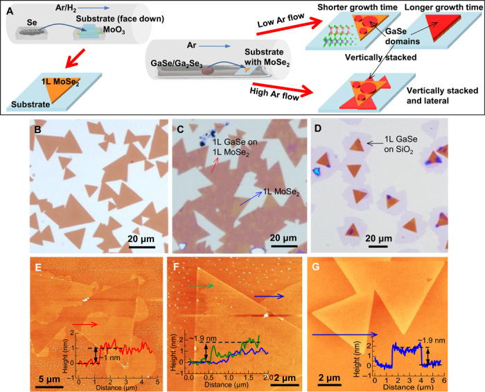
(A) Schematic illustrating the growth of 1L MoSe2 and GaSe/MoSe2 heterostructures. (B) Optical micrograph of 1L MoSe2 triangular flakes and domains of merged triangles grown on a SiO2/Si substrate. (C) Optical micrograph of 1L GaSe domains (with reddish color contrast as indicated by a red arrow) grown on 1L MoSe2 domains (as indicated by a blue arrow). (D) Optical micrograph of 1L GaSe domains grown on 1L MoSe2 and laterally from the side of 1L MoSe2 on SiO2/Si substrates (as indicated by a black arrow). (E and F) AFM images showing GaSe domains grown on and from the side of 1L MoSe2 flakes. Insets are height profiles along the red, blue, and green lines, indicating that the GaSe domains grown vertically and laterally on MoSe2 are monolayer. (G) AFM image showing 1L GaSe fully covering 1L MoSe2 flakes, as indicated by the height profile along the blue solid line.
As suggested in previous work, the ratio of the deposition to diffusion rate is a key parameter in the growth process and determines the average distance that an adsorbed species has to travel to meet another adsorbate, either for nucleation of a new aggregate or attachment to an already formed island (34). At low argon gas flow rates, we hypothesize that the deposition rate of GaSe molecules is slower than the diffusion rate required for the growth of GaSe to occur at near-equilibrium conditions. In this case, the adsorbed GaSe molecules can explore the potential energy surface to reach a minimum energy configuration. According to the Ehrlich-Schwoebel barrier step-edge growth mechanism, the diffusion of molecules over a terrace has a lower energy barrier than diffusion along an edge, and descending an edge is often an energetically more costly process than terrace diffusion (35). Therefore, the GaSe molecules adsorbed on the SiO2 surface could diffuse over MoSe2 steps and find the minimum energy locations on the MoSe2 surface, forming a vertical heterostructure. When the argon gas flow rate is increased, however, the deposition rate can exceed the diffusion rate, and the growth of GaSe will be essentially determined by kinetics. This makes it possible to form more nucleation sites on the surface and suppress the diffusion processes of adsorbed GaSe molecules, leading to the growth of GaSe/MoSe2 lateral heterostructures on SiO2/Si.
The detailed atomic structures of the vertically stacked and lateral GaSe/MoSe2 heterostructures were investigated using annular dark-field (ADF) imaging in an aberration-corrected scanning transmission electron microscope (STEM). Figure 2A shows an ADF-STEM image highlighting the edges of a 1L GaSe domain stacked on 1L MoSe2. The morphology of the edge area (highlighted by red dashed lines in Fig. 2A) indicates that the growth of GaSe monolayers on MoSe2 may proceed with the evolution of sharp edges, oriented with neighboring contiguous islands at 60° angles (see fig. S3, C and D, as well) (27). Figure 2B shows the atomic structure of the stacking region along the [001] direction. We observed Moiré patterns which are caused by the interference of the lattice between MoSe2 and GaSe. The periodicity of one Moiré pattern was estimated to be ~2.63 nm (highlighted by red dashed rhombuses), indicating the formation of a periodic superlattice. Figure 2D shows the fast Fourier transform (FFT) of the as-acquired image (Fig. 2B). Two different sets of diffraction patterns can be distinguished: one corresponding to the GaSe lattice (lattice constant a = 0.375 nm) and the other corresponding to the MoSe2 lattice (lattice constant a = 0.329 nm), indicating single-crystal GaSe and MoSe2, and a large lattice misfit (13%). The well-aligned registry between the GaSe and MoSe2 monolayers demonstrated by the diffraction pattern (Fig. 2D) indicates that the irregularly shaped GaSe domains are grown on MoSe2 through vdW epitaxy. Figure S4 shows an atomic-resolution ADF-STEM image with an enlarged view on the region around the edge of GaSe domain, which further demonstrates the vdW epitaxy of 1L GaSe governed by the underlying MoSe2 monolayer.
Fig. 2. Atomic structure of the vertically stacked GaSe/MoSe2 vdW heterostructure.
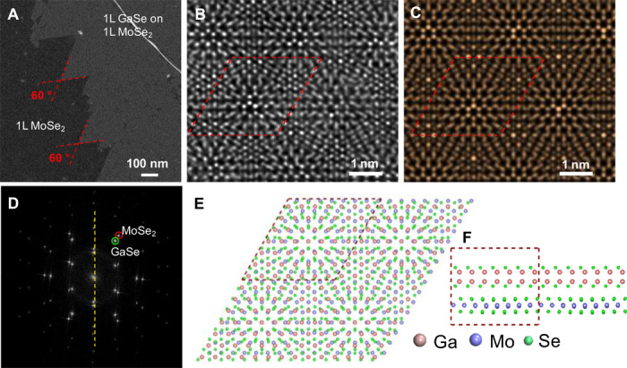
(A) Low-magnification ADF-STEM image showing the edge area of the 1L GaSe domain grown on 1L MoSe2. (B and C) Experimental (B) and simulated (C) atomic-resolution ADF-STEM image showing the atomic structure of the periodic superlattice where 1L GaSe stacks on top of 1L MoSe2. The red dashed rhombuses indicate the unit cell of the GaSe/MoSe2 heterostructure (supercell), with a lattice constant of L = 2.63 nm. (D) FFT pattern obtained from (B). (E and F) Top view and side view of the calculated atomic model of the GaSe/MoSe2 vdW heterostructure, respectively. The supercell is demarcated by the red dashed lines.
Density functional theory (DFT) calculations show that the lattice constant of the smallest repeating cell in the epitaxially stacked GaSe/MoSe2 heterostructure is ~2.625 nm (7 × 7 GaSe/8 × 8 MoSe2; Fig. 2, E and F), consistent with the lattice constant determined by experiments (Fig. 2B). The binding energy of the supercell was calculated to be ~11.51 eV (corresponding to 117 meV/GaSe), suggesting that the vdW interaction is strong in these heterostructures. The simulated STEM image (Fig. 2C) derived from the well-aligned GaSe/MoSe2 model optimized by DFT (Fig. 2E) reproduces the periodic Moiré patterns observed experimentally, further confirming the epitaxial nature of the vertically stacked GaSe/MoSe2 vdW heterostructures. Epitaxy of the vertically stacked GaSe/MoSe2 vdW heterostructure was also confirmed by electron diffraction in large scale (fig. S3) and is consistent among all domains that were examined with 1L GaSe on top of MoSe2. It should be pointed out that from the ideal lattice constant, the two materials should be incommensurate with an infinite supercell size (no periodicity). However, the STEM results clearly show a periodic superlattice with a lattice constants of ~2.63 nm, and the lattice constants of GaSe and MoSe2 are slightly changed from their ideal values. This is further confirmed by our calculations that a supercell size around ~2.63 nm maintains the smallest lattice strain among all supercell configurations.
Although GaSe grew strictly along the lattice orientation of the underlying MoSe2 in the vertically stacked GaSe/MoSe2 heterostructures, 1L GaSe domains grown laterally near the edge of the 1L MoSe2 flakes (on amorphous SiO2) always showed misalignment at random angles with respect to the lattice orientation of the MoSe2 (figs. S3, A and B, and S5, A to C). Furthermore, no atomically sharp boundaries between the two lattices were observed (fig. S5D). These results suggest that epitaxial edge growth between largely misfit lattices (monolayer GaSe and MoSe2) may be difficult, presumably due to the high formation energy of the boundaries between the monolayer GaSe and MoSe2. We note that electrical current can hardly be detected across the junction of this lateral GaSe/MoSe2 because of the disordered region at the boundary (figs. S5D and S6).
Figure 3 (A and B) shows a monolayer lateral GaSe/MoSe2 heterostructure sitting on top of another MoSe2 layer. The brighter region shown in Fig. 3A is the bilayer MoSe2 region, whereas the less bright region corresponds to the vdW epitaxial GaSe on top of the monolayer MoSe2 that extended from the bilayer region. As shown in the inset of Fig. 3A, the optical image corresponding to such a structure is observed consistently. In this case, the GaSe domain followed the registry of the underlying MoSe2 layer and thus has the same in-plane lattice orientation with the nearby MoSe2 layer during the growth. An atomic-resolution image of the interface region (highlighted by the white dashed rectangle in Fig. 3A) is shown in Fig. 3B. The FFT pattern (inset of Fig. 3B) confirms the same lattice orientation between the 1L GaSe and MoSe2 layers across the interface region. An overlapping region between the 1L GaSe and 2L MoSe2 is clearly seen because of the brighter intensity in the middle of the image. To further determine the morphology of the overlapping region, inverse FFT is used to separate the GaSe epitaxial layer from the MoSe2 lattice (fig. S7). Figure 3 (C and D) shows the inverse FFT images of the 1L GaSe (Fig. 3C) and MoSe2 (Fig. 3D) layers highlighted in the red rectangle in Fig. 3B. A step edge of the MoSe2 layers can be identified, as marked by the yellow dashed line in Fig. 3D. Remarkably, both Ga and Se atomic columns in the 1L GaSe epitaxial layer show an elliptical shape inside a distorted hexagonal lattice before the step edge of MoSe2, as highlighted by the green dashed rectangle in Fig. 3C. The elliptical shape and lattice distortion can be attributed to a local inclination region in the GaSe epitaxial film, as illustrated by the schematic in Fig. 3E. The inclination misaligns the two atoms in Ga or Se atomic columns when viewing along the [001] direction, which leads to the elliptical shape of the atomic columns due to displacement between the two atoms in the projected plane. These results indicate that this lateral GaSe/MoSe2 is different from previously reported edge-epitaxial MX2/MX2 heterostructures with direct lateral connections and edge epitaxy (19–22), and further demonstrate that an atomically sharp lateral boundary between GaSe and MoSe2 layers is presumably not energy-favorable, even though they share the same lattice orientation. Instead, the GaSe epitaxial layer prefers to buckle up and overlap the MoSe2 layer to form a vertically stacked vdW heterostructure, which is more stable than forming direct lateral bonding with MoSe2.
Fig. 3. Atomic structure of the lateral GaSe/MoSe2 heterostructure.
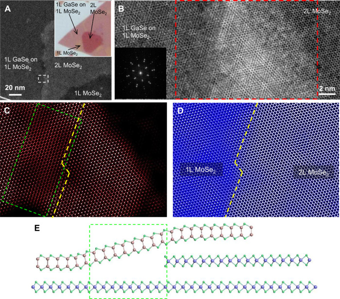
(A) Low-magnification ADF-STEM image showing a 1L GaSe domain connected laterally to a 1L MoSe2 domain where such a heterostructure sits on top of another 1L MoSe2 as an underlying substrate and follows its lattice orientation. Inset: Optical micrograph showing a similar structure in large scale (the red triangle is the 2L MoSe2 region). (B) Atomic-resolution ADF-STEM image of the area highlighted in the white dashed rectangle in (A), showing an overlapping region between the 1L GaSe domain and the bilayer MoSe2 in the lateral connection region (highlighted by the red dashed rectangle). (C and D) Inverse FFT images of 1L GaSe and MoSe2 layers in (B). The green dashed rectangle in (C) highlights the inclined region. The yellow dashed lines in (C) and (D) indicate the position of the step edge in the MoSe2 layers. (E) Schematic of the overlapping structure in the lateral connection region that shows the buckling of 1L GaSe (on 1L MoSe2) stacks on top of the second MoSe2 layer.
The optical properties of the vertically stacked GaSe/MoSe2 vdW heterostructures were studied with Raman and PL spectroscopy in backscattering mode through a microscope equipped with a long-distance objective (~1-μm spot size) and 532-nm laser excitation. Figure 4A shows an optical micrograph of 1L MoSe2 flakes partially covered by GaSe domains with different thicknesses (note that multilayer GaSe domains are occasionally observed, and the exact number of layers is revealed by the AFM image in fig. S8). Figure 4B shows Raman spectra acquired from a bare 1L MoSe2 region and a GaSe/MoSe2 heterostructure with 1L, 3L, and ~15L GaSe. The four spectra show three typical Raman modes for 1L MoSe2, that is, the dominant A1g mode (out-of-plane, 240.6 cm−1) and the weak E1g and E12g modes (in-plane, ~148 and ~287 cm−1, respectively) (36). The peak positions of the three MoSe2 modes do not shift, but the intensities of the E1g and E12g modes slightly increase with GaSe grown on top. The Raman spectrum of GaSe/MoSe2 with ~15L GaSe also shows characteristic GaSe peaks corresponding to the A11g (133.4 cm−1), E12g (212.8 cm−1), and A21g (~306 cm−1) vibrational modes (Fig. 4B, orange curve; see also the magnified spectra shown in fig. S8A) (4, 37, 38). The intensity of the three peaks decreases prominently as the thickness of the GaSe layers is reduced, and the A11g and E12g peaks were hardly observed for 1L GaSe on MoSe2 (Fig. 4B and fig. S9A, red curves), which is similar to GaSe atomic layers grown on amorphous SiO2 (4). However, the GaSe epitaxial layers on MoSe2 show enhancement of the E21g Raman peak as the number of layers decreases (an enlarged view is provided in fig. S9), which was not observed from GaSe atomic layers grown on amorphous SiO2 (4). The E21g vibration mode of GaSe, generally located at ~244 cm−1 for very thick (>30L) crystals (4), is not detected in the crystals with ~15L GaSe (Fig. 4B, orange curve), but it shows up at 258.7 cm−1 for 3L GaSe (Fig. 4B, blue curve) and is even enhanced in 1L GaSe (Fig. 4B, red curve). This phenomenon was also observed in our previous work, wherein vdW GaSe epitaxial layers were synthesized on graphene (27). The enhancement of Raman modes in both MoSe2 and GaSe in the vdW heterostructure may be due to strong interlayer charge transfer (fig. S10) (27).
Fig. 4. Optical properties of the GaSe/MoSe2 vdW heterostructure.
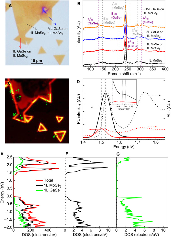
(A) Optical micrograph showing 1L MoSe2 islands and flakes with partially covered GaSe domains. The corresponding AFM image shown in fig. S8 was used to measure the number of layers in the GaSe domains. (B) Raman spectra obtained from regions of bare 1L MoSe2 and GaSe domains with different layer numbers on MoSe2 as shown in (A). The excitation source is a 532-nm laser. Note that the spectra were offset for clarity. AU, arbitrary units. (C) PL emission mapping of the area corresponding to (A) with excitation from a 532-nm laser and integrated emission intensity from 700 to 900 nm. (D) PL emission and absorption spectra of bare 1L MoSe2 and 1L GaSe/1L MoSe2 vdW heterostructures. Black solid curve: PL spectrum corresponding to the inner region of bare 1L MoSe2 (spots 1, 2, and 3). Red solid curve: PL spectrum corresponding to the inner region of bare 1L GaSe/1L MoSe2 (spots 7 and 8). The inset shows an enlarged view from 1.6 to 1.8 eV. The PL spectra from the edge area (spots 4, 5, 6, 9, and 10) are shown in fig. S11. Black dashed curve: absorption spectrum of bare 1L MoSe2. Red dashed curve: absorption spectrum of 1L GaSe/1L MoSe2. The absorption spectra were normalized to their A exciton peak. (E) DOS 1L GaSe/1L MoSe2 vdW heterostructure (red solid curve) using DFT calculations. The valence band maximum (VBM) is set at 0 eV. The black and green solid curves are contributions from 1L MoSe2 and 1L GaSe, respectively. (F and G) DOS of independent 1L MoSe2 and 1L GaSe using DFT calculations. The VBM is set at 0 eV.
The interactions between GaSe and MoSe2 layers also influence the PL of vertically stacked GaSe/MoSe2 vdW heterostructures. Figure 4C shows a PL emission intensity map (integrated from 700 to 900 nm) corresponding to the optical micrograph in Fig. 4A. The emission intensities decrease significantly in the regions covered by GaSe layers compared to those with bare 1L MoSe2. The edges of MoSe2 show stronger PL than the inner regions of the crystals. The enhancement of emission intensity at the edges is also accompanied by a blue shift of the emission bands (fig. S11), which is observed on the edges of the MoSe2 with and without GaSe layers. Therefore, we believe that the enhanced and blue-shifted emission at the edge is not due to the growth of GaSe layers, but may be caused by several factors including the dielectric environment, adsorbates, or defects (39). We also note that some previously reported CVD-grown MoSe2 monolayers show decreased PL energy and red-shifted PL energy at the edge (40). Considering the different growth conditions reported by Wang et al. (40) (growth under ambient pressure) from those in our work (growth under low pressure), the resulting monolayers may have different defect states or dielectric interactions at their edges, which could possibly induce different trends in the PL.
The PL emission spectra obtained from typical spots (inner regions of bare 1L MoSe2 and 1L GaSe/1L MoSe2) in the map are shown in Fig. 4D (solid curves). For bare 1L MoSe2 (Fig. 4D, black solid curve), the dominant emission band peaking at 1.524 eV (~814 nm) and a much weaker band located at ~1.707 eV (~727 nm) (inset of Fig. 4D) correspond to the recombination of the A and B excitons. The absorption bands for the A and B excitons in 1L MoSe2 also appear on the absorption spectrum (Fig. 4D, black dashed curve), from which a slight Stokes shift (~0.01 eV) of the emission spectrum can be seen. The emission and absorption spectra of the 1L GaSe/1L MoSe2 heterostructure (Fig. 4D, red solid and dashed curves) show A and B exciton bands similar to those of bare 1L MoSe2, but with a red shift (~0.024 eV) and smaller emission intensity (resulting in the darker regions on PL mapping, Fig. 1C). No emission and absorption bands from 1L GaSe were detected because of its indirect bandgap (4), an observation that was confirmed by the absorption spectra of bare 1L GaSe (fig. S12). These spectral results indicate that the band structure close to the valence and conduction band edge of the heterostructure maintains the characteristics of 1L MoSe2. The experimental results are consistent with the density of states (DOS) of the GaSe/MoSe2 vdW heterostructure calculated by DFT (Fig. 4E), from which the conduction band minimum (CBM) of the heterostructure is attributed to MoSe2, and the valence band maximum (VBM) is attributed to a mixed contribution from MoSe2 and GaSe. The heterostructure maintains the direct bandgap of 1L MoSe2, but with a flatter valence band edge due to the contribution of 1L GaSe (fig. S13). Compared to 1L MoSe2 and 1L GaSe (Fig. 4, F and G), the band structure changes and the bandgap shrinks for 1L MoSe2 and 1L GaSe in the vdW heterostructure as a result of strong interlayer coupling (the bandgap decreases from 1.4 to 1.35 eV for MoSe2 and from 1.8 to 1.45 eV for GaSe). It should be noted that the absolute values of bandgap are underestimated in DFT calculations, but the relative trend is correct. The reduced bandgap energy of the heterostructure results in red-shifting the PL and absorption bands (Fig. 4D), and the observed quenching of the PL in the heterostructure can be attributed to the spontaneous separation of charge carriers between layers that decreases the electron-hole recombination rate (11). This is commensurate with the PV effect of the heterostructure, which is discussed later.
To study the electrical and optoelectronic properties of the GaSe/MoSe2 vdW heterostructure, field-effect transistor devices were fabricated by patterning source-drain contacts (Ti/Au) on a 1L MoSe2 flake partially covered by 1L GaSe domains. Note that a SiO2/(p++)Si substrate was used for growth and back-gating, and the final device is shown in Fig. 5A. As shown in Fig. 5A, electrodes 1 and 2 were deposited on top of GaSe/MoSe2, whereas electrode 3 was deposited on the adjacent bare MoSe2 region. The transfer characteristic of the vdW heterostructure as a whole (by measuring current between electrodes 1 and 2) shows ambipolar behavior (Fig. 5B) and is attributed to the p-type GaSe and n-type MoSe2. The heterostructure also has high threshold voltages at both the p side and the n side (~30 and ~40 V, respectively). Under white light illumination (power density, ~64.42 mW/cm2 from 400 to 800 nm) and a back-gate voltage of zero (Vbg = 0 V), the heterostructure shows a strong photocurrent (PC). Under chopped illumination (inset of Fig. 5B), the device exhibited a stable PC with an ON/OFF ratio of ~215 and a reproducible photoresponsivity of ~30 mA/W [calculated under a source-drain voltage (Vds) of 5 V with a device area of ~15 μm2].
Fig. 5. Electrical and optoelectronic properties of the GaSe/MoSe2 vdW heterostructure.
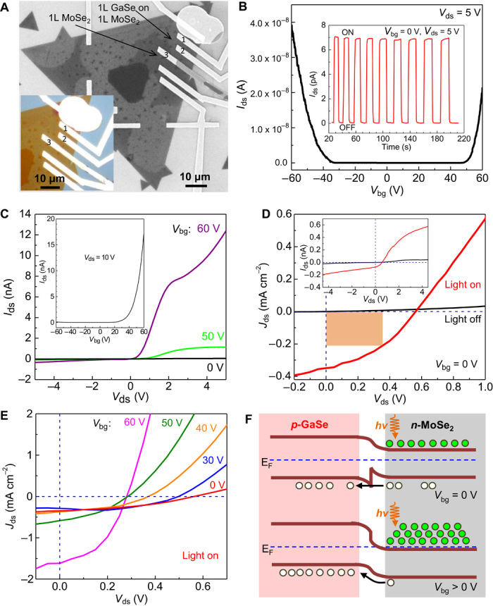
(A) SEM image of a device made on a 1L MoSe2 partially covered by 1L GaSe domains. Electrodes 1 and 2 were made on the GaSe/MoSe2 vdW heterostructure region, whereas electrode 3 was made on a bare 1L MoSe2 region. Inset shows the corresponding optical micrograph. (B) Ids-Vbg curve (with Vds fixed at 5 V) of the vdW heterostructure as a whole measured using electrodes 1 and 2 (without illumination). The inset shows the time-resolved photoresponse of the vdW heterostructure at Vbg = 0 V and Vds = 5 V using a white light source. (C) Ids-Vds curves across the p (GaSe)–n (MoSe2) heterojunction (measured using electrodes 2 and 3) at different back-gate voltages (without illumination). The inset shows the Ids-Vbg curve (with Vds fixed at 10 V) across the heterojunction. (D) Jds-Vds curves (Vbg = 0 V) with (red solid curve) and without (black solid curve) white light illumination across the heterojunction. The area with orange shading indicates Pmax. The inset shows the Ids-Vds curves on a larger scale. (E) Jds-Vds curves with white light illumination across the heterojunction at different back-gate voltages. (F) Equilibrium band diagram of the GaSe/MoSe2 heterojunction at Vbg = 0 V (upper) and Vbg > 0 V (lower) with light illumination.
The electrical and optoelectronic properties of the p (GaSe)–n (MoSe2) heterojunction were measured using electrodes 2 and 3. The output curve (Ids-Vds) is gate-dependent and clearly shows current rectification behavior (Fig. 5C), indicating that a good p-n diode is formed across the heterojunction. The transfer characteristic is n-type dominant (inset of Fig. 5C), indicating that MoSe2 dominates the charge transport across the heterojunction. Gate-tunable output curves and photovoltaic response were observed under white light illumination and different back-gate voltages ranging from 0 to 60 V (Fig. 5, D and E; see fig. S14 as well). At Vbg = 0 V, the output curve (the red solid curve in Fig. 5, D and E) showed an open-circuit voltage (Voc) of ~0.57 V and a short-circuit current density (Jsc) of ~0.35 mA/cm2 (device area, ~21 μm2). As the back-gate voltage was increased, the Voc value decreased, reaching ~0.28 V at Vbg = 60 V, whereas the Jsc value generally increased, reaching ~1.62 mA/cm2 at Vbg = 60 V (Fig. 5E). The solar energy conversion performances of the heterojunction, including the photon-to-electron conversion efficiency, fill factor, and photoresponsivity (at Vds = 0 V), were estimated to be 0.12%, 0.38, and 5.5 mA/W, respectively, at Vbg = 0 V, and these values increased to 0.3%, 0.43, and 25.3 mA/W, respectively, at Vbg = 60 V.
In the GaSe/MoSe2 vdW heterojunction, the overlying 1L GaSe generally served as a transparent window material (41) because of its very weak absorption of visible light (fig. S12), and therefore, the photoresponse process takes place in MoSe2. According to the band alignment of GaSe and MoSe2 across the heterojunction (Fig. 5E), at zero back-gate voltage, the CBM of GaSe lies at a higher energy than that of MoSe2, whereas the VBM of the two materials is at approximately the same energy level (Fig. 5F, upper diagram). The photogenerated charge carriers in MoSe2 undergo spontaneous charge separation, in which the electrons remain in MoSe2, whereas the holes are transported to the p-type side, that is, GaSe (Fig. 5F, upper diagram, and fig. S10). The charge separation is also proven by quenched PL from the heterostructure (Fig. 4, C and D). The gate-tunable photovoltaic response could be due to several factors. First, a back-gate voltage induces an excess carrier concentration that reduces the carrier lifetime and increases recombination of photogenerated carriers (11, 42, 43). However, the band of MoSe2 is pulled down at positive back-gate voltages, causing more band bending and different band alignments that enhance the charge separation and collection across the heterojunction (Fig. 5F, lower diagram). The decrease of Voc and the increase of Isc as Vbg increases could be the result of the competition between these two factors.
DISCUSSION
In summary, we have demonstrated that despite a large lattice misfit, monolayers of GaSe grow by vdW epitaxy on MoSe2 to form bilayer heterojunctions with atomically sharp interfaces and well-defined, large supercells. This misfit bilayer heterojunction coupling p-type and hole-transporting GaSe with n-type and highly photoresponsive MoSe2 results in a gate-tunable photovoltaic response with effective transfer and separation of photogenerated charge carriers. Such GaSe/MoSe2 misfit bilayers therefore appear to be promising building blocks for 2D solar cells, despite relatively low efficiencies, which may be improved by optimizing growth conditions to increase the quality of the GaSe epitaxial layers (to reduce resistivity) and by applying an optimized device design. Although the lateral 1L GaSe/MoSe2 heterostructures were typically found not to have an epitaxial alignment between lattices, a proper substrate that could simultaneously define the orientation of both lattices via vdW epitaxy may enable the reliable synthesis of monolayer lateral heterojunctions with well-aligned lattices. The successive CVD approach demonstrated here for the vdW epitaxial growth of well-defined heterojunctions involving different compounds appears promising for the reliable synthesis of new bilayers of misfit layer compound “building blocks” to enrich the library of functional 2D systems for next-generation optical, electrical, and optoelectronic devices.
MATERIALS AND METHODS
Materials synthesis
The GaSe/MoSe2 heterostructures were fabricated through a two-step synthesis process. The 2D MoSe2 flakes were first synthesized through a CVD method conducted in a tube furnace system equipped with a 2″ quartz tube. In a typical run, the growth substrates, for example, Si with 250 nm SiO2 (SiO2/Si) cleaned by acetone and isopropanol (IPA), were placed facedown above an alumina crucible containing ~0.2 g of MoO3 powder, which was then inserted into the center of the quartz tube. Another crucible containing ~1.2 g of Se powder was located at the upstream side of the tube. After evacuating the tube to ~5 × 10⁻³ torr, flows of 40 sccm argon and 6 sccm hydrogen gas were introduced into the tube, and the reaction was conducted at 780°C (with a ramping rate of 30°C/min) for 5 min at a reaction chamber pressure of 20 torr. At 780°C, the temperature at the location of the Se powder was ~290°C. After growth, the furnace was cooled naturally to room temperature. The as-synthesized MoSe2 was used as templates for the growth of 2D GaSe, which was carried out in a tube furnace system equipped with a 1″ quartz tube. Bulk GaSe crystals (synthesized as described in our previous work) and Ga2Se3 powder were mixed together (GaSe/Ga2Se3 molar ratio, ~50:1) and were used as source materials. In a typical run, ~60 mg of the source powder and the substrate with the as-synthesized 2D MoSe2 flakes were loaded on a quartz boat and subsequently inserted into the furnace. The source was located at the center of the furnace, with the substrate located ~8 to 10 cm downstream. After evacuating the tube to ~5 × 10⁻³ torr, the reaction was conducted at 750°C (with a ramping rate of 20°C/min) for 2 to 5 min at a pressure of 30 torr and an argon carrier gas flow rate of 40 to 50 sccm. The vapor-phase reactants were transported by the flowing argon gas to the growth region, in which the temperature was ~710° to 720°C, thereby feeding the growth of the 2D GaSe crystals. After growth, the furnace was cooled naturally to room temperature. With 40 sccm argon gas flow, only vertical stacking GaSe/MoSe2 was obtained, whereas as the flow rate was increased to 50 sccm, both vertical and lateral GaSe/MoSe2 were obtained.
Characterization
The morphologies of the GaSe/MoSe2 heterostructures were characterized using optical microscopy (Leica DM4500 P), SEM (Zeiss Merlin SEM), and AFM (Bruker Dimension Icon AFM).
The atomic-resolution structures of the GaSe/MoSe2 heterostructures were investigated using ADF-STEM in an aberration-corrected Nion UltraSTEM operating at 60 kV, using a half-angle range of the ADF detector from 86 to 200 mrad. All ADF-STEM images were low-pass–filtered to increase the signal-to-noise ratio. Figure 2B was deconvoluted with a proper Gaussian probe function for better visibility. The interlayer orientation of vertical stacking GaSe/MoSe2 was also examined by electron diffraction in a FEI Technai T12 transmission electron microscope (TEM) operating at 100 kV. The samples for STEM and TEM analyses were transferred onto silicon TEM grids coated with amorphous 5-nm-thick silicon films. For sample transfer, poly(methyl methacrylate) (PMMA) was first spun onto the SiO2/Si substrate with GaSe/MoSe2 heterostructures at 3500 rpm for 60 s. The PMMA-coated substrate was then floated on 1 M KOH solution that etched the silica epi-layer, leaving the PMMA film with the heterostructures floating on the solution surface. The film was transferred to deionized water several times to remove residual KOH and then scooped onto the Si TEM grid. PMMA was removed by acetone and baking in vacuum at 300°C for 2 hours.
Raman and PL measurements were conducted using a home-built micro-Raman/PL setup, which included an upright microscope coupled to a spectrometer (Spectra Pro 2300i, Acton; f = 0.3 m, 150 grooves/mm grating) equipped with a charge-coupled device camera (Pixis 256BR, Princeton Instruments). The excitation source was a continuous wave laser (1-mW laser power, λ = 532 nm) focused to a spot of ~1 μm using a long-distance objective (100×, numerical aperture = 0.8). The Raman and PL signals were collected through the 100× objective, and the spectra were recorded using LightField software (Princeton Instruments).
Device fabrication and measurements
Electron beam lithography (FEI DB-FIB with Raith pattern writing software) was used for GaSe/MoSe2 heterojunction device fabrication. First, a layer of PMMA 495A4 was spun-coat on the SiO2 (250 nm)/Si substrate with GaSe/MoSe2 heterojunctions followed by a 180°C bake. After pattern writing and development, a 10-nm layer of Ti followed by a 50-nm layer of Au was deposited using electron beam evaporation. Finally, well-defined source and drain electrodes were revealed using a lift-off process with acetone/IPA. The electrical and optoelectronic properties of the heterostructures were measured in vacuum (~10−6 torr) under a probe station using a semiconductor analyzer (Keithley 4200) and a laser-driven white light source with a power density of 1.2 mW/cm2 from 400 to 800 nm.
Theoretical calculation
All DFT calculations were performed using the VASP (Vienna Ab initio Simulation Package) code (44). The projector augmented wave potentials were used to describe the core electrons, and the generalized gradient approximation with the Perdew-Burke-Ernzerhof (PBE)–type functional was selected in our calculations. The effect of vdW interactions was taken into account by using the PBE+ vdW scheme, and the self-consistent electron density was used to calculate C6 coefficients (45). The kinetic energy cut for the plane-wave basis was set to 400 eV. The structure was fully relaxed until the force on each atom was less than 0.01 eV/A.
Supplementary Material
Funding
Synthesis science was sponsored by the Materials Science and Engineering Division, Office of Basic Energy Sciences, U.S. Department of Energy (DOE). Materials characterization was conducted at the Center for Nanophase Materials Sciences, which is a DOE Office of Science User Facility. X.L. and M.-W.L. acknowledge support from Oak Ridge National Laboratory Directed Research and Development. S.T.P. and J.L. acknowledge the support from the DOE through grant DE-FG02-09ER46554. W.Z. was supported by the Materials Sciences and Engineering Division, Office of Basic Energy Sciences, DOE. Author contributions: X.L. and K.X. designed the research. K.X. and D.B.G. supervised the research. X.L. synthesized the materials and conducted optical microscope, SEM, and AFM characterizations. M.-W.L., I.K., and J.F. fabricated the device, and M.-W.L. conducted electrical and optoelectronic measurements. J.L., W.Z., and S.T.P. conducted ADF-STEM characterizations and data analysis. B.H. performed theoretical calculation and atomic structure modeling. A.A.P. conducted Raman and PL characterizations and data analysis. C.M. and M.C. conducted TEM and electron diffraction measurements. C.M.R. and K.W. contributed to the CVD setup and materials synthesis. All authors discussed the results and contributed to the writing of the manuscript. Competing interests: The authors declare that they have no competing interests. Data and materials availability: All data used to obtain the conclusions in this paper are presented in the paper and/or the Supplementary Materials. Other data may be requested from the authors.
SUPPLEMENTARY MATERIALS
Supplementary material for this article is available at http://advances.sciencemag.org/cgi/content/full/2/4/e1501882/DC1
Fig. S1. AFM image of MoSe2 monolayers.
Fig. S2. SEM and AFM images of GaSe/MoSe2 vdW heterostructures.
Fig. S3. TEM and electron diffraction analyses of the GaSe/MoSe2 vdW heterostructure.
Fig. S4. Structural analyses of the GaSe/MoSe2 vdW heterostructure.
Fig. S5. Structure of lateral 1L GaSe/MoSe2 on the SiO2/Si substrate.
Fig. S6. Electrical performance of the monolayer GaSe/MoSe2 lateral junction grown on SiO2/Si.
Fig. S7. Structural analyses of lateral 1L GaSe/MoSe2 on 1L MoSe2.
Fig. S8. AFM image corresponding to the optical image in Fig. 4A.
Fig. S9. Enlarged view of Raman spectra shown in Fig. 4B.
Fig. S10. Calculation of charge transfer between intrinsic GaSe and MoSe2 monolayers.
Fig. S11. PL emission spectra of MoSe2 and GaSe/MoSe2 vdW heterostructures, obtained from PL emission mapping in Fig. 4A.
Fig. S12. Absorption spectra of monolayer GaSe grown on transparent mica.
Fig. S13. DFT calculation of the band structure of the GaSe/MoSe2 vdW heterostructure.
Fig. S14. Ids-Vds curves under white light illumination across the heterojunction at different back-gate voltages.
REFERENCES AND NOTES
- 1.Butler S. Z., Hollen S. M., Cao L., Cui Y., Gupta J. A., Gutiérrez H. R., Heinz T. F., Hong S. S., Huang J., Ismach A. F., Johnston-Halperin E., Kuno M., Plashnitsa V. V., Robinson R. D., Ruoff R. S., Salahuddin S., Shan J., Shi L., Spencer M. G., Terrones M., Windl W., Goldberger J. E., Progress, challenges, and opportunities in two-dimensional materials beyond graphene. ACS Nano 7, 2898–2926 (2013). [DOI] [PubMed] [Google Scholar]
- 2.Radisavljevic B., Radenovic A., Brivio J., Giacometti V., Kis A., Single-layer MoS2 transistors. Nat. Nanotechnol. 6, 147–150 (2011). [DOI] [PubMed] [Google Scholar]
- 3.Hu P., Wang L., Yoon M., Zhang J., Feng W., Wang X., Wen Z., Idrobo J. C., Miyamoto Y., Geohegan D. B., Xiao K., Highly responsive ultrathin GaS nanosheet photodetectors on rigid and flexible substrates. Nano Lett. 13, 1649–1654 (2013). [DOI] [PubMed] [Google Scholar]
- 4.Li X., Lin M.-W., Puretzky A. A., Idrobo J. C., Ma C., Chi M., Yoon M., Rouleau C. M., Kravchenko I. I., Geohegan D. B., Xiao K., Controlled vapor phase growth of single crystalline, two-dimensional GaSe crystals with high photoresponse. Sci. Rep. 4, 5497 (2014). [DOI] [PMC free article] [PubMed] [Google Scholar]
- 5.Morkoç H., Mohammad S. N., High-luminosity blue and blue-green gallium nitride light-emitting diodes. Science 267, 51–55 (1995). [DOI] [PubMed] [Google Scholar]
- 6.P. S. Zory Jr., Quantum Well Lasers (Academic Press, San Diego, CA, 1993). [Google Scholar]
- 7.Pospischil A., Furchi M. M., Mueller T., Solar-energy conversion and light emission in an atomic monolayer p-n diode. Nat. Nanotechnol. 9, 257–261 (2014). [DOI] [PubMed] [Google Scholar]
- 8.Ross J. S., Klement P., Jones A. M., Ghimire N. J., Yan J., Mandrus D. G., Taniguchi T., Watanabe K., Kitamura K., Yao W., Cobden D. H., Xu X., Electrically tunable excitonic light-emitting diodes based on monolayer WSe2 p–n junctions. Nat. Nanotechnol. 9, 268–272 (2014). [DOI] [PubMed] [Google Scholar]
- 9.Geim A. K., Grigorieva I. V., Van der Waals heterostructures. Nature 499, 419–425 (2013). [DOI] [PubMed] [Google Scholar]
- 10.Fang H., Battaglia C., Carraro C., Nemsak S., Ozdol B., Kang J. S., Bechtel H. A., Desai S. B., Kronast F., Unal A. A., Conti G., Conlon C., Palsson G. K., Martin M. C., Minor A. M., Fadley C. S., Yablonovitch E., Maboudian R., Javey A., Strong interlayer coupling in van der Waals heterostructures built from single-layer chalcogenides. Proc. Natl. Acad. Sci. U.S.A. 111, 6198–6202 (2014). [DOI] [PMC free article] [PubMed] [Google Scholar]
- 11.Lee C.-H., Lee G.-H., van der Zande A. M., Chen W., Li Y., Han M., Cui X., Arefe G., Nuckolls C., Heinz T. F., Guo J., Hone J., Kim P., Atomically thin p–n junctions with van der Waals heterointerfaces. Nat. Nanotechnol. 9, 676–681 (2014). [DOI] [PubMed] [Google Scholar]
- 12.Cheng R., Li D., Zhou H., Wang C., Yin A., Jiang S., Liu Y., Chen Y., Huang Y., Duan X., Electroluminescence and photocurrent generation from atomically sharp WSe2/MoS2 heterojunction p–n diodes. Nano Lett. 14, 5590–5597 (2014). [DOI] [PMC free article] [PubMed] [Google Scholar]
- 13.Chiu M.-H., Zhang C., Shiu H.-W., Chuu C.-P., Chen C.-H., Chang C.-Y. S., Chen C.-H., Chou M.-Y., Shih C.-K., Li L.-J., Determination of band alignment in the single-layer MoS2/WSe2 heterojunction. Nat. Commun. 6, 7666 (2015). [DOI] [PMC free article] [PubMed] [Google Scholar]
- 14.Rivera P., Schaibley J. R., Jones A. M., Ross J. S., Wu S., Aivazian G., Klement P., Seyler K., Clark G., Ghimire N. J., Yan J., Mandrus D. G., Yao W., Xu X., Observation of long-lived interlayer excitons in monolayer MoSe2–WSe2 heterostructures. Nat. Commun. 6, 6242 (2015). [DOI] [PubMed] [Google Scholar]
- 15.Hong X., Kim J., Shi S.-F., Zhang Y., Jin C., Sun Y., Tongay S., Wu J., Zhang Y., Wang F., Ultrafast charge transfer in atomically thin MoS2/WS2 heterostructures. Nat. Nanotechnol. 9, 682–686 (2014). [DOI] [PubMed] [Google Scholar]
- 16.Tongay S., Fan W., Kang J., Park J., Koldemir U., Suh J., Narang D. S., Liu K., Ji J., Li J., Sinclair R., Wu J., Tuning interlayer coupling in large-area heterostructures with CVD grown MoS2 and WS2 monolayers. Nano Lett. 14, 3185–3190 (2014). [DOI] [PubMed] [Google Scholar]
- 17.Withers F., Pozo-Zamudio O. D., Mishchenko A., Rooney A. P., Gholinia A., Watanabe K., Taniguchi T., Haigh S. J., Geim A. K., Tartakovskii A. I., Novoselov K. S., Light-emitting diodes by band-structure engineering in van der Waals heterostructures. Nat. Mater. 14, 301–306 (2015). [DOI] [PubMed] [Google Scholar]
- 18.Liu L., Park J., Siegel D. A., McCarty K. F., Clark K. W., Deng W., Basile L., Idrobo J. C., Li A.-P., Gu G., Heteroepitaxial growth of two-dimensional hexagonal boron nitride template by graphene edges. Science 343, 163–167 (2014). [DOI] [PubMed] [Google Scholar]
- 19.Gong Y., Lin J., Wang X., Shi G., Lei S., Lin Z., Zou X., Ye G., Vajtai R., Yakobson B. I., Terrones H., Terrones M., Tay B. K., Lou J., Pantelides S. T., Liu Z., Zhou W., Ajayan P. M., Vertical and in-plane heterostructures from WS2/MoS2 monolayers. Nat. Mater. 13, 1135–1142 (2014). [DOI] [PubMed] [Google Scholar]
- 20.Huang C., Wu S., Sanchez A. M., Peters J. J. P., Beanland R., Ross J. S., Rivera P., Yao W., Cobden D. H., Xu X., Lateral heterojunctions within monolayer MoSe2–WSe2 semiconductors. Nat. Mater. 13, 1096–1101 (2014). [DOI] [PubMed] [Google Scholar]
- 21.Duan X., Wang C., Shaw J., Cheng R., Chen Y., Li H., Wu X., Tang Y., Zhang Q., Pan A., Jiang J., Yu R., Huang Y., Duan X., Lateral epitaxial growth of two-dimensional layered semiconductor heterojunctions. Nat. Nanotechnol. 9, 1024–1030 (2014). [DOI] [PMC free article] [PubMed] [Google Scholar]
- 22.Li M.-Y., Shi Y., Cheng C.-C., Lu L.-S., Lin Y.-C., Tang H.-L., Tsai M.-L., Chu C.-W., Wei K.-H., He J.-H., Chang W.-H., Suenaga K., Li L.-J., Epitaxial growth of a monolayer WSe2-MoS2 lateral p-n junction with an atomically sharp interface. Science 349, 524–528 (2015). [DOI] [PubMed] [Google Scholar]
- 23.Haigh S. J., Gholinia A., Jalil R., Romani S., Britnell L., Elias D. C., Novoselov K. S., Ponomarenko L. A., Geim A. K., Gorbachev R., Cross-sectional imaging of individual layers and buried interfaces of graphene-based heterostructures and superlattices. Nat. Mater. 11, 764–767 (2012). [DOI] [PubMed] [Google Scholar]
- 24.Shi Y., Zhou W., Lu A.-Y., Fang W., Lee Y.-H., Hsu A. L., Kim S. M., Kim K., Yang H. Y., Li L.-J., Idrobo J.-C., Kong J., Van der Waals epitaxy of MoS2 layers using graphene as growth templates. Nano Lett. 12, 2784–2791 (2012). [DOI] [PubMed] [Google Scholar]
- 25.Lin Y.-C., Lu N., Perea-Lopez N., Li J., Lin Z., Peng X., Lee C. H., Sun C., Calderin L., Browning P. N., Bresnehan M. S., Kim M. J., Mayer T. S., Terrones M., Robinson J. A., Direct synthesis of van der Waals solids. ACS Nano 8, 3715–3723 (2014). [DOI] [PubMed] [Google Scholar]
- 26.Lin Y.-C., Chang C.-Y. S., Ghosh R. K., Li J., Zhu H., Addou R., Diaconescu B., Ohta T., Peng X., Lu N., Kim M. J., Robinson J. T., Wallace R. M., Mayer T. S., Datta S., Li L.-J., Robinson J. A., Atomically thin heterostructures based on single-layer tungsten diselenide and graphene. Nano Lett. 14, 6936–6941 (2014). [DOI] [PubMed] [Google Scholar]
- 27.Li X., Basile L., Huang B., Ma C., Lee J., Vlassiouk I. V., Puretzky A. A., Lin M.-W., Yoon M., Chi M., Idrobo J. C., Rouleau C. M., Sumpter B. G., Geohegan D. B., Xiao K., Van der Waals epitaxial growth of two-dimensional single-crystalline GaSe domains on graphene. ACS Nano 9, 8078–8088 (2015). [DOI] [PubMed] [Google Scholar]
- 28.R. Tsu, Superlattice to Nanoelectronics (Elsevier, Oxford, UK, 2010). [Google Scholar]
- 29.Hunt B., Sanchez-Yamagishi J. D., Young A. F., Yankowitz M., LeRoy B. J., Watanabe K., Taniguchi T., Moon P., Koshino M., Jarillo-Herrero P., Ashoori R. C., Massive Dirac fermions and Hofstadter butterfly in a van der Waals heterostructure. Science 340, 1427–1430 (2013). [DOI] [PubMed] [Google Scholar]
- 30.Ponomarenko L. A., Gorbachev R. V., Yu G. L., Elias D. C., Jalil R., Patel A. A., Mishchenko A., Mayorov A. S., Woods C. R., Wallbank J. R., Mucha-Kruczynski M., Piot B. A., Potemski M., Grigorieva I. V., Novoselov K. S., Guinea F., Fal’ko V. I., Geim A. K., Cloning of Dirac fermions in graphene superlattices. Nature 497, 594–597 (2013). [DOI] [PubMed] [Google Scholar]
- 31.Merrill D. R., Moore D. B., Bauers S. R., Falmbigl M., Johnson D. C., Misfit layer compounds and ferecrystals: Model systems for thermoelectric nanocomposites. Materials 8, 2000–2029 (2015). [DOI] [PMC free article] [PubMed] [Google Scholar]
- 32.Panchakarla L. S., Radovsky G., Houben L., Popovitz-Biro R., Dunin-Borkowski R. E., Tenne R., Nanotubes from misfit layered compounds: A new family of materials with low dimensionality. J. Phys. Chem. Lett. 5, 3724–3736 (2014). [DOI] [PubMed] [Google Scholar]
- 33.Li H., Duan X., Wu X., Zhuang X., Zhou H., Zhang Q., Zhu X., Hu W., Ren P., Guo P., Ma L., Fan X., Wang X., Xu J., Pan A., Duan X., Growth of alloy MoS2xSe2(1−x) nanosheets with fully tunable chemical compositions and optical properties. J. Am. Chem. Soc. 136, 3756–3759 (2014). [DOI] [PubMed] [Google Scholar]
- 34.Barth J. V., Costantini G., Kern K., Engineering atomic and molecular nanostructure at surfaces. Nature 437, 671–679 (2005). [DOI] [PubMed] [Google Scholar]
- 35.Ganapathy R., Buckley M. R., Gerbode S. J., Cohen I., Direct measurements of island growth and step-edge barriers in colloidal epitaxy. Science 327, 445–448 (2010). [DOI] [PubMed] [Google Scholar]
- 36.Tonndorf P., Schmidt R., Böttger P., Zhang X., Börner J., Liebig A., Albrecht M., Kloc C., Gordan O., Zahn D. R. T., Michaelis de Vasconcellos S., Bratschitsch R., Photoluminescence emission and Raman response of monolayer MoS2, MoSe2, and WSe2. Opt. Express 21, 4908–4916 (2013). [DOI] [PubMed] [Google Scholar]
- 37.Lei S., Ge L., Liu Z., Najmaei S., Shi G., You G., Lou J., Vajtai R., Ajayan P. M., Synthesis and photoresponse of large GaSe atomic layers. Nano Lett. 13, 2777–2781 (2013). [DOI] [PubMed] [Google Scholar]
- 38.Zhou Y., Nie Y., Liu Y., Yan K., Hong J., Jin C., Zhou Y., Yin J., Liu Z., Peng H., Epitaxy and photoresponse of two-dimensional GaSe crystals on flexible transparent mica sheets. ACS Nano 8, 1485–1490 (2014). [DOI] [PubMed] [Google Scholar]
- 39.Peimyoo N., Shang J., Cong C., Shen X., Wu X., Yeow E. K. L., Yu T., Nonblinking, intense two-dimensional light emitter: Monolayer WS2 triangles. ACS Nano 7, 10985–10994 (2013). [DOI] [PubMed] [Google Scholar]
- 40.Wang X., Gong Y., Shi G., Chow W. L., Keyshar K., Ye G., Vajtai R., Lou J., Liu Z., Ringe E., Tay B. K., Ajayan P. M., Chemical vapor deposition growth of crystalline monolayer MoSe2. ACS Nano 8, 5125–5131 (2014). [DOI] [PubMed] [Google Scholar]
- 41.A. Aruchamy, Photoelectrochemistry and Photovoltaics of Layered Semiconductors (Kluwer Academic Publishers, Dordrecht, 1992). [Google Scholar]
- 42.Furchi M. M., Pospischil A., Libisch F., Burgdörfer J., Mueller T., Photovoltaic effect in an electrically tunable van der Waals heterojunction. Nano Lett. 14, 4785–4791 (2014). [DOI] [PMC free article] [PubMed] [Google Scholar]
- 43.Lee G.-H., Lee C.-H., van der Zande A. M., Han M., Cui X., Arefe G., Nuckolls C., Heinz T. F., Hone J., Kim P., Heterostructures based on inorganic and organic van der Waals systems. APL Mater. 2, 092511 (2014). [Google Scholar]
- 44.Kresse G., Furthmüller J., Efficiency of ab-initio total energy calculations for metals and semiconductors using a plane-wave basis set. Comput. Mater. Sci. 6, 15–50 (1996). [DOI] [PubMed] [Google Scholar]
- 45.Tkatchenko A., Scheffler M., Accurate molecular van der Waals interactions from ground-state electron density and free-atom reference data. Phys. Rev. Lett. 102, 073005 (2009). [DOI] [PubMed] [Google Scholar]
Associated Data
This section collects any data citations, data availability statements, or supplementary materials included in this article.
Supplementary Materials
Supplementary material for this article is available at http://advances.sciencemag.org/cgi/content/full/2/4/e1501882/DC1
Fig. S1. AFM image of MoSe2 monolayers.
Fig. S2. SEM and AFM images of GaSe/MoSe2 vdW heterostructures.
Fig. S3. TEM and electron diffraction analyses of the GaSe/MoSe2 vdW heterostructure.
Fig. S4. Structural analyses of the GaSe/MoSe2 vdW heterostructure.
Fig. S5. Structure of lateral 1L GaSe/MoSe2 on the SiO2/Si substrate.
Fig. S6. Electrical performance of the monolayer GaSe/MoSe2 lateral junction grown on SiO2/Si.
Fig. S7. Structural analyses of lateral 1L GaSe/MoSe2 on 1L MoSe2.
Fig. S8. AFM image corresponding to the optical image in Fig. 4A.
Fig. S9. Enlarged view of Raman spectra shown in Fig. 4B.
Fig. S10. Calculation of charge transfer between intrinsic GaSe and MoSe2 monolayers.
Fig. S11. PL emission spectra of MoSe2 and GaSe/MoSe2 vdW heterostructures, obtained from PL emission mapping in Fig. 4A.
Fig. S12. Absorption spectra of monolayer GaSe grown on transparent mica.
Fig. S13. DFT calculation of the band structure of the GaSe/MoSe2 vdW heterostructure.
Fig. S14. Ids-Vds curves under white light illumination across the heterojunction at different back-gate voltages.