Abstract
A complete high-efficiency transmit amplifier unit designed to be implemented in on-coil transmit arrays is presented. High power capability, low power dissipation, scalability and cost minimization were some of the requirements imposed to the design. The system is composed of a current mode class-D (CMCD) amplifier output stage and a voltage mode class-D (VMCD) preamplification stage. The amplitude information of the radio frequency pulse was added through a customized step-down DC-DC converter with current amplitude feedback that connects to the CMCD stage. Benchtop measurements and imaging experiments were carried out to analyze system performance. Direct control of B1 was possible and its load sensitivity was reduced to less than 10% variation from unloaded to full loaded condition. When using the amplifiers in an array configuration, isolation above 20 dB was achieved between neighboring coils by the amplifier decoupling method. High output current operation of the transmitter was proved on the benchtop through output power measurements and in a 1.5 T scanner through flip angle quantification. Finally, single and multiple channel excitations with the new hardware were demonstrated by receiving signal with the body coil of the scanner.
Introduction
Multi-channel transmit systems appear to be a promising solution to the B1 non-uniformities [1–5] and increased specific absorption rate (SAR) present at high field imaging (B0 > 3 T) [6–8]. Additionally, transmit arrays with sufficient number of elements allow for selective excitation patterns [9,10] and B0 corrections [11,12]. These promising advantages have led to the design of transmit arrays with a high number of elements [10,13,14]. However, building these arrays by simply replicating multiple standard single-transmit setups potentially results in a very high system cost and complexity, which only grows if practical issues are considered such as tuning, matching and decoupling each of the elements in the array. Furthermore, cable coupling and mechanical stress have to be considered due to multiple power radio frequency (RF) cables connecting to the coil. Therefore, the replacement of the standard single transmit element by a large multi-element transmit system requires the design of new hardware that makes the system scalable and cost-effective. In recent years, different RF transmit amplifier configurations have been proposed to be implemented in multi-element transmit arrays [15–22].
A novel approach that significantly rethinks the transmit setup is locating the RF amplifier system directly on the coil [15–18]. Since amplification is now performed on the coil, only small power RF signals are transmitted to the coil-amplifier system, avoiding the large RF power coaxial cables that are currently present in standard transmit system. This relieves the mechanical constraints encountered at the time of building a multi-element transmit array as well as potentially reducing cable coupling. Importantly, the on-coil amplifier configuration exploits the intrinsic output impedance of the active devices of the amplifier for decoupling with neighboring elements, similar to preamplifier decoupling in receiver arrays [23]. Additionally, on-coil current-mode amplifiers present the advantage of allowing direct control of the B1 field [17,18], potentially making the system independent of patient-coil interaction, thus tuning and matching the coil with different loads is unnecessary. It is important to note that in this setup the on-coil amplifiers would be in close proximity with the patient, which makes the minimization of the heat dissipation an additional requirement to the system. For this application, switch-mode configurations potentially provide improved performance over linear amplifiers since they have higher power efficiency and lower heat dissipation [24–26]. In this work, we present a novel high efficiency switch-mode on-coil transmit amplifier system and demonstrate its use in MRI applications. Each amplifier module has a voltage-mode class-D (VMCD) pre-amplification stage and current-mode class-D (CMCD) power output stage modulation of the RF pulse is added to the unit by implementing a customized current-feedback switch-mode power supply as the voltage source of the CMCD output stage [27]. In addition, we demonstrate how this amplifier can be controlled directly with fiber optic cables, thus greatly reducing the cabling complexity for large scale parallel transmit arrays. Workbench measurements and imaging experiments with multiple parallel transmitters are performed to show the performance of the proposed system.
Theory
RF CMCD Amplifier
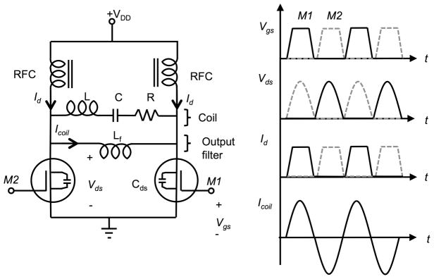
Figure 1 shows a CMCD amplifier circuit diagram, and its voltage and current waveforms, where the active devices are metal-oxide semiconductor field effect transistors (MOSFETs) in push-pull configuration. Each device conducts only during half a cycle, thus driving a differential current through the load. The devices operate in current mode by fixing the amplitude of the drain current in an RF cycle through RF chokes connected to a voltage supply (VDD). The MOSFETs are controlled by a differential signal with frequency set at the desired output frequency.
Figure 1.
Schematic Diagram of the CMCD stage. Voltage and current waveforms for MOSFET 1 (M1) and MOSFET 2 (M2) are shown in solid line and grey dash line respectively. The resonant filter formed by Lf and Cds filters out higher harmonics from the drain current source and the fundamental component is recovered on the coil.
Ideally, a MOSFET has two states where there are low losses: fully off, such that no current is flowing, or fully on, where there can be high currents, but with low intrinsic resistance within the MOSFET. At RF frequencies these two pure states are difficult to achieve because the output capacitance of the MOSFET (Cds) is non-negligible, and it must be compensated to achieve high power efficiency. To this end, the CMCD amplifier contains a parallel band-stop filter, with resonance at the frequency of interest, formed by and external inductor located between the drain terminals in parallel with the load (which in our case is the MR coil) and Cds [18]. This filter makes it possible to implement zero voltage switching (ZVS), which greatly improves power efficiency. ZVS ensures that the drain-source voltage is zero at switching time. Therefore, power losses due to the charge and discharge of the MOSFET output capacitance are avoided during switching transitions [24]. This allows for a nearly ideal switching between the two low-loss states of the MOSFET, which greatly improves the efficiency of the amplifier as a whole. In addition to compensating for the output capacitance, this filter behaves as a high impedance pathway at the resonance frequency and as very low impedance at all other frequencies, such that higher harmonics are filtered out from the load.
While inefficiencies due to the output capacitance are removed, there are still losses due to the drain-source resistance of the device (RDS.ID2) that can be reduced as gate voltage is increased. The total current at the drain terminal (ID) is the sum of the fundamental and the odd harmonic components that result from the current-mode switch-mode operation. To ensure optimum push-pull switching amplification, high-amplitude 180° out-of-phase voltage signals are necessary at the MOSFET gates. As described below, these were implemented in our configuration with a pre-amplification stage using a more traditional VMCD stage.
Voltage and current waveforms of the CMCD output stage (Fig. 1) are reversed to those in a VMCD. Ideally there is no overlap between current and voltage at the drain, which would reduce the switching losses to zero. The current is ideally square in shape through the MOSFET, but the output resonant filter allows attenuation of the odd higher harmonics and thus only the fundamental component is driven through the load.
RF envelope generation
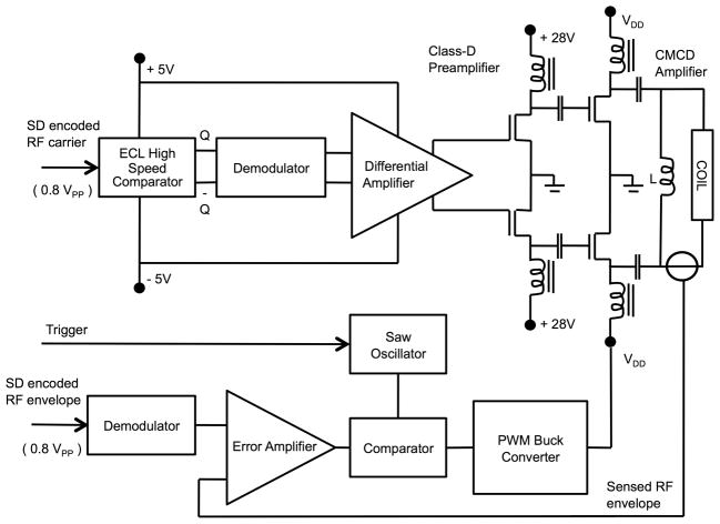
To add the RF envelope information to the output RF pulse while keeping the power-efficient switching topology of the system [28], a Pulse Width Modulation (PWM) controlled step-down (Buck) converter [29] was designed and interfaced at the voltage source of the CMCD stage (Fig. 2). The output voltage of this converter is proportional to a high DC input voltage (VIN) weighted by the duty cycle of a power MOSFET switch that connects VIN to a LC filter that storages energy to be driven to the load (CMCD stage) and filters out the switching frequency component and its harmonics that fall outside the bandwidth of interest. The duty cycle of the converter is set by the comparison of a saw tooth clock signal (of frequency at least ten times the desired RF envelope bandwidth) and an error signal that results from the difference of a target and measured RF envelope. The duty cycle is then dynamically adjusted such that the amplitude of the fundamental RF current in the coil tracks the target amplitude (or envelope) independently of the load condition (note that the RF envelope bandwidth is far below the RF carrier frequency) [30]. For example, if the target is higher than the sensed signal the on-time of the MOSFET will increase (higher duty cycle) and more power will be driven to the output to increase the amplitude of the envelope. The drain voltage of the CMCD stage will be modulated by this amplified version of the signal envelope allowing shaped pulses to be transmitted to the coil. In addition, the effect of this modulation on the MOSFETs impedance has to be taken into account as it is described later in the text. The envelope information was recovered by sensing the RF current by a loop magnetically coupled to the amplifier output and estimating the actual output amplitude information through rectification and filtering. This current feedback and the high output impedance of the amplifier aided by the resonant filter makes it possible to represent the amplifier as a current source.
Figure 2.
Schematic diagram of the complete RF amplifier unit.
Materials and Methods
Hardware Design
Signal Source and Fiber Optic Transmission
One significant advantage of the on-coil CMCD amplifier stage is that the low level RF signals can be brought directly to the amplifier using a fiber optic cable, which greatly simplifies the cabling requirements by eliminating any cable coupling. To achieve efficient transmission down the fiber, both RF carrier and envelope were encoded using sigma delta modulation (SDM) [31]. Unlike other pulse density modulation techniques, SDM allows digital transmission at high SNR through noise-shaping that reduces quantization noise in the bandwidth of interest such that high resolution digital conversion is possible even at low oversampling rates [32]. This offers great advantages versus conventional ADC when sampling high rate signals as the RF carrier. Additionally, SDM allows digital-analog conversion through simple filtering.
To implement SDM, RF carrier and envelope were encoded in MATLAB using the SDM toolbox and synthesized by a data-timing generator (DTG; Tektronix DTG7058 750 Mb/s) at 512 Mb/s (oversampling of 4x). Each signal was transmitted through a separate fiber optic cable connected between a fiber optic transmitter and a receiver (Agilent HFBR-5720LP 1.0625 GBd), the latter mounted on the transmit array. The RF carrier was demodulated on the amplifier board through a 3rd order Butterworth band-pass filter with center frequency at 63.6 MHz and an 11 MHz bandwidth. While the RF envelope signal, with expected bandwidth up to hundreds of kHz, was demodulated through a 5th order low-pass Butterworth filter with 4 MHz cutoff frequency.
Current Mode Class-D Amplifier and Preamplifier
The SDM encoded RF carrier is amplified and split into two 180° out-of-phase digital signals through a high speed Emitter Coupled Logic (ECL) comparator (Analog Devices ADCMP565). It is then demodulated through the band-pass filter with center frequency at 63.6 MHz. The demodulated signal is amplified by a cascade of two high-speed differential amplifiers (Analog Devices AD8132) with approximately 15 dB of total voltage gain. In order to efficiently switch the power MOSFETs in the CMCD stage, a two stage VMCD preamplifier further amplifies the voltage and current. The first lower power stage comprises two dual-gate N-MOSFETs (Philips Semiconductor BF998), while the second stage consists of two RF power N-MOSFETs (M/A-COM MRF160).
For the CMCD power output stage we used the dual RF N-MOSFET MRF275G (M/A-COM semiconductor) that has a guaranteed 500 MHz bandwidth, 26 A ID_MAX and parasitic capacitance in the 100 pF range. To generate shaped RF pulse, the drain voltage was modulated by the DC-DC converter. Because of the variable output capacitance of the MOSFET, the effect of this modulation on the amplifier operation needed to be considered. This voltage-modulated drain-source capacitance has an impact on the performance of the output filter. Thus, to select the appropriate value of filter inductance (LF), different values were tested to resonate the drain-source capacitance Cds (estimated as Cds= Coss − Crss from the manufacturer’s datasheet) at 63.66 MHz at different drain voltage values. Current mode operation was set by connecting RF chokes from the MOSFET’s drain terminals to the power supply. In both preamplification and amplification stages, the MOSFETs were connected in push-pull class-D configuration.
As mentioned before, in this amplifier design RF amplitude and frequency information are separated. Therefore, a high amplitude RF carrier could be still present at the gate of the output MOSEFTs even when no drain bias is applied at the CMCD stage as it would be in the case of the zero crossings of a sinc pulse. At the operating frequency, this can produce RF leakage through the non-negligible gate-drain capacitance (approximately 100 pF at VDD = 0 V). To reduce this effect the RF carrier was modulated at the encoding stage such that the value was zero when the RF envelope was below 0.1% of its maximum peak. We tested the performance of the system with and without this modulation.
The digital interface, preamplifier and amplifier were designed together in a 4-layer PCB board to enhance stability of the system by shielding DC networks from RF side, while the Buck converter and PWM controller board was mounted on a daughter board 2 cm over the amplifier.
Amplitude Modulation (AM) System and Current Feedback
A customized Buck converter (DC-DC down conversion) controlled by PWM was designed to power the CMCD stage. The frequency of the converter was set close to 2 MHz to have a maximum stable control bandwidth of approximately 200 kHz. The LC output filter consisted of a customized inductor of value approximately 4 μH and a SMPS ceramic 3 μF capacitor. These values were set initially to limit output voltage ripple below 0.2 V at 50% duty cycle for a nominal input voltage of 60 V at an estimated maximum load of 10 A. A discrete PWM controller was designed that set the duty cycle of the PWM signal based on the comparison of the target RF envelope and a sensed version of the RF envelope. The target RF envelope was obtained from amplification and demodulation of the sigma-delta encoded RF envelope (ΔΣ) in similar way as it was performed for the demodulation of the RF carrier. While current could be directly sensed on a segment of the RF coil [19], it was found that a better option to avoid extra cables is to sense the amplifier output current directly using a 5 mm diameter, 6-turn wire loop magnetically coupled to one of the output traces on the amplifier board (Fig. 2). The size and number of turns of the sensor was determined empirically to have enough measurement sensitivity to track the zero-point of the RF envelope. By properly positioning the loop on the output trace, the induced voltage at the loop terminals was an attenuated version of the output modulated RF current. A simple half-wave rectifier formed by a Schottky diode followed by a low-pass filter with cutoff frequency below the resonance frequency (63.6 MHz) was used to recover the envelope information. This signal was scaled and connected to the inverting input of an error amplifier (Texas Instruments, TLE2142C) whose non-inverting input was connected to the target RF envelope. An adjustable zero compensation circuit composed of a resistor-capacitance (RC) series network was added between the output and inverting input of the error amplifier to assure stability while maintaining a large enough bandwidth for the current application (in the kHz range). The output of the error amplifier was the error feedback signal that was compared with a saw wave of 1.7 MHz frequency generated by a timing circuit (Texas Instruments, TLC551). This comparison generated the PWM signal that is connected to a high-voltage half-bridge MOSFET driver (National Semiconductor LM5104) to control the switching of the power MOSFETs of the Buck converter. The performance of the system was analyzed for different target envelopes by measuring the resulting modulated RF pulse through a pick-up loop coupled to the coil and connected to the oscilloscope (Agilent DS07104B). High-power bandwidth was tested by transmitting a sinc pulse of fixed number of zero-crossing points and variable pulse length and peak amplitude corresponding to approximately 3 A peak output current. Peak–to-peak voltage per B1 magnetic field (VPP/B1) was measured by a pick-up loop connected to the oscilloscope through a 10 dB attenuator. PWM duty cycle and output voltage of the converter (VDD) were measured for three different envelope amplitudes when the input voltage of the converter (VIN) was set approximately to 60 V. At this conditions, output power and efficiency were also measured as detailed in the next section.
Benchtop Measurements
Peak Power, Current and Power Dissipation
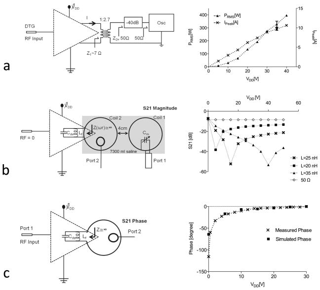
Given that the output of the amplifier is not 50 Ω and that the amplifier is designed for driving small non-reactive loads, power measurement was not straightforward in this configuration. Therefore, different measurements were attempted to estimate these values, in addition to MRI experiments. In a first setup, in order to estimate maximum power capability of the CMCD amplifier stage alone, the AM system was bypassed and power was controlled directly by manually changing the VDD value while transmitting a 500 μs hard pulse. An impedance transformer that down-converted a 50 Ω load into few ohms was connected at the amplifier output to simulate its normal operation when driving current to the coil. The resulting turn ratio was 1:2.7 giving a primary impedance of Z1 = 6.6 Ω − j400 mΩ at 63.66 MHz after resonating the primary parasitic reactance with a series capacitor. Copper losses introduced by the transformer winding were minimized by increasing the wire cross-sectional area and reducing the number of primary and secondary turns for the required turn ratio. To measure output power, the secondary of the transformer was connected to the 50 Ω input impedance of the oscilloscope through a 40 dB attenuator and the primary winding was connected to the output of the CMCD stage [Fig. 3(a)]. Output power of one amplifier was measured indirectly by measuring the RMS voltage on the 50 Ω load. In this setup, the duty cycle of the excitation was limited to 0.1% to protect the attenuators such that 1 kW of pulsed power results in 1 W dissipation. RMS current at the output of the CMCD stage was calculated indirectly from the power measurement by including the primary resistance of the transformer.
Figure 3.
Peak power and current measurement using an impedance transformer connected to the CMCD output that loads amplifier with approximately 7 Ω when a 50 Ω load is connected to the secondary winding and drain voltage is changed manually across the expected operating range (a). Inter-element isolation of two non-overlapping coils vs. drain voltage provided by the amplifier’s output impedance. Isolation varies with voltage due to the voltage-modulated drain-source capacitance Cds of the power MOSFET (b). Effect of this modulation on the phase of the RF carrier (c).
To evaluate operation of the complete system, the CMCD module was connected to the DC-DC converter as in normal operation and its output connected to the impedance transformer as described above. For five different RF envelope’s peak amplitudes, RF output voltage, DC current and voltage supply to CMCD stage (converter output) and PWM duty cycles were measured with the oscilloscope to calculate RMS power and drain efficiency. Mean and standard deviation (SD) of the different variables were estimated from three replicates. These measurements were performed while transmitting the same 500 μs pulse but this time at 0.5 % duty cycle. In addition to efficiency estimations and to evaluate heating dissipation that could result from the amplifier operation, temperature was measured with an infrared thermometer (Extech IR-Enabled EX470 Multimeter) on a region of the amplifier board next to the power MOSFETs; expected hottest spot closest to the patient. Temperature was monitored while running the amplifier on the benchtop in same setup as in the case of imaging with the cylindrical array (i.e.; RF pulse, duty cycle and loading condition). We also measured temperature in a more extreme condition, while the amplifier was driven with 500 μs hard pulse at 50% duty cycle and drain voltage set such that output current was approximately 5 A peak. The amplifier was left working at this condition for at least 5 minutes to reach a stable temperature reading.
Inter-element decoupling
To analyze the intrinsic decoupling offered by the amplifier system, isolation was measured between two coils (coil 1 and coil 2) of size 12 cm x12 cm, tuned at 63.6 MHz, separated by 4 cm of distance and loaded with a 7300 ml saline phantom [Fig. 3(b)]. This coil separation was set smaller than the expected distance to a next neighbor element (approximately 8 cm for this coil size) when the nearest neighbor is overlapped in order to test the performance with significant potential coupling. In a first setup, both coils were matched to 50 Ω as it would be in a conventional system and isolation was estimated from the transmission parameter S21 measured through a network analyzer (Agilent Technologies, E5061A) with coil 1 connected to port 1 and coil 2 terminated with 50 Ω and coupled to a pick-up loop connected to port 2. In a second setup, the matching capacitor of coil 2 was removed and the coil was connected to the output of a CMCD amplifier with its RF input set to zero. Note that the output filter in the CMCD stage is key for decoupling since high impendence is seen from the coil into the amplifier output at its resonance frequency. This frequency is determined by the external inductor and Cds which value is reduced as drain voltage is increased. In normal operation of the amplifier, the drain voltage of the output MOSFETs is adjusted continuously by the AM system to track the desired RF envelope, such that the effects of this modulation on decoupling have to be analyzed at different output levels. Isolation measurements were therefore performed while manually changing the supply voltage of the CMCD output stage (the AM system was bypassed) and repeated for different value of output filter resonances by changing the external inductor value.
Decoupling of this coil-phantom setup, with both coils driven by CMCD amplifiers with amplitude current feedback, was evaluated through imaging by transmitting with one element at a time and with both elements simultaneously. Image acquisition was performed as detailed in the Imaging section.
Phase of RF carrier
To analyze how the phase of the RF carrier was modified by the amplifier system, port 1 of the network analyzer transmitting at 63.6 MHz was set as the input of the amplifier and the RF output was measured though a pick-up loop coupled to the coil and connected through a 30 dB attenuator to port 2 [Fig 3(c)]. The on-coil amplifier has a high speed broadband 50 Ω matched comparator at its input, so no modification on the amplifier design was needed for this measurement setup. In this configuration, the forward transmission parameter (S21) phase was measured for different values of drain voltage as performed for the decoupling measurements. Even though the amplifier system has a cascade of MOSFETs through the different stages that can add phase to the RF carrier, only the MOSFETs in the CMCD stage were expected to produce a dynamic change of the phase due to the change in drain-source capacitance value with the low frequency drain voltage modulation added by the AM system. To further understand the phase behavior of the RF signal a model of the CMCD stage was simulated in MATLAB using the capacitor-drain voltage characteristic curve provided by the MOSFET manufacturer.
Load Sensitivity
Load sensitivity analysis of an amplifier module (amplifier and AM system) was performed by measuring the change in B1 field for a constant input while changing the distance of a 1500 ml saline phantom to the coil. B1 was measured by a pick-up loop lightly coupled to the output coil tuned at 63.6 MHz and connected to the oscilloscope (Agilent Technologies DS06054A), and therefore it is reported in units of VPP/B1. The distance was increased in steps of 2 cm until no difference in voltage was noted from the non-loaded condition. This measurement was performed while transmitting a 1ms Gaussian pulse and VPP/B1 was measured at the peak.
Transmit only coil array implementation
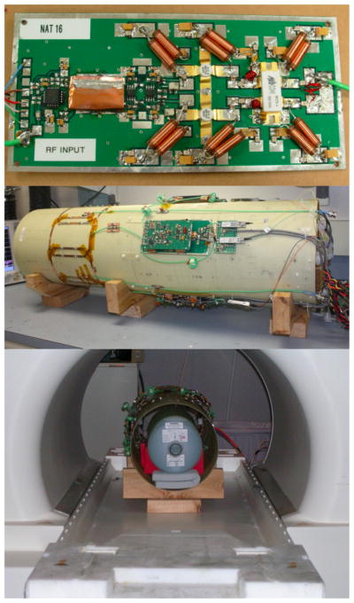
A coil array made of eight elements was built on a cylindrical FR4 former of 25 cm diameter by using copper tape of 6 mm thickness. Because of limitations in our present digital drive configuration, only four elements (every other element with a 90° azimuthal angle between them) were used in these experiments. Photographs of one amplifier module, the cylindrical array and its setup in the scanner are shown in Fig. 4. Tuning and decoupling were performed by measuring S11 and S21 parameters with the network analyzer. The coils were tuned to 63.6 MHz and decoupling between coils was achieved through amplifier decoupling. Since the MOSFETs in the current amplifier prototype and the optical receivers are slightly magnetic, the modules were positioned 20 cm from the coil through a coaxial cable to avoid any susceptibility artifact when imaging. The input impedance of coil-cable setup as seen by the amplifier at the resonant condition when the coil array was loaded with a 7300 ml saline phantom was approximately 3 Ω + j12 Ω. Note that for the case of the two-element array in planar configuration this impedance was approximately 7 Ω after resonating the cable reactance with a series capacitor.
Figure 4.
Photograph of RF amplifier board (top), the cylindrical array with the complete system assembled (middle) and its setup in scanner (bottom).
Due to the wide range of values of Cds as a function of drain voltage, and the effect of this modulation on amplifier decoupling, two separate modes of operation were implemented in the current array. The primary mode of operation was an RF shimming array where each channel transmits essentially the same waveform. In this case the value of LF is set so as to have high decoupling during high power simultaneous transmission and ensuring high attenuation of harmonics (Cds resonated at VDD = 15 V). For the purposes of analyzing the characteristics of this array, it was also implemented a mode where each element can transmit independently, for example, to generate B1 maps for individual elements. In this case, using same resonance condition for the output filter, the decoupling during the single channel transmission mode was improved by a small DC voltage bias at the drain of the inactive amplifiers such as to reduce its output capacitance value and to obtain a similar resonance condition as in the case of simultaneous operation. Practically the single channel transmission mode was implemented through a jumper that connected the drain of the inactive amplifier/s connected to a 5 V line bypassing the AM modulation system. Because of the load insensitivity and direct current drive of this amplifier configuration, this mode of operation would not normally be required, since it can be configured once and then used for all subsequent exams.
The array was controlled by four digitally encoded envelope signals and four RF carrier signals sent independently from the DTG outputs through fiber optic cables to the each amplifier board. The relative phases among channels were measured on the benchtop by setting the phase of the first channel as reference. In this setup, port 1 of the network analyzer was set as the RF carrier input of each of the amplifier while port 2 was connected to a pick-up loop coupled to the corresponding coil. S21 phase values were measured for each channel referred to channel 1 phase while transmitting a hard pulse, and any phase correction was implemented in the signal encoding process such that all channels have the same initial phase. Amplitude calibration was also performed on the benchtop by sending an SDM encoded signal of equal amplitude to each of the amplifiers and adjusting the feedback gain in the PWM converter such as to read same VPP/B1 at the center of each coil.
Imaging
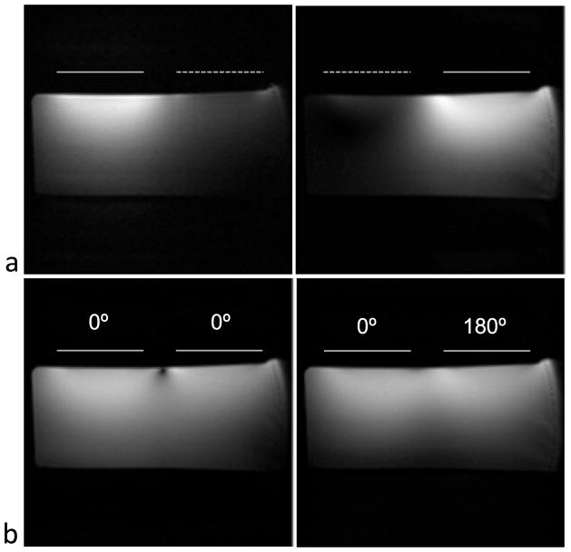
The transmit system was used on a 1.5 T clinical MRI scanner (Espree, Siemens) using the body coil as the receiver while the RF transmission from the scanner was disabled by disconnecting the small RF signal from the input of the scanner RF power amplifier. The DTG was synchronized with the scanner 10 MHz clock and triggered by the RF unblank TTL signal. The +5 V and −5 V DC voltage lines that connect to the comparator and differential amplifiers of the transmit system, and the +5 V line that connects to the fiber optic receiver (same line used to bias the drain of inactive amplifiers when needed) were triggered outside the acquisition window since these devices generated considerable noise in images when left powered during reception. Images of a 7300 ml saline cylindrical phantom were acquired with a gradient echo sequence with 2 ms windowed sinc RF pulse excitation, 100 ms TR, 10 ms TE, 10 mm slice thickness, 25 x 25 cm2 FOV, and single average. This sequence was used to acquire single and multiple channel images. Since our goal was to construct a prototype that could be used for RF shimming applications, the same waveform was sent to all elements in this initial implementation. We tested a homogenous mode by phasing each element as its azimuthal angle (0°, 90°, 180°, 270°) and a gradient mode where the phase of successive channels was inverted (0°, 180°, 0°, 180°). Flip angle and B1 information were acquired through the double angle method [33] by transmitting with one channel and using the same GRE sequence at a longer TR of 3 s to reduce T1 and T2 (approximately 200 ms) weighting. Images of the two-coil setup presented in Fig. 3(b) were acquired using same sequence and with the phantom’s long axis aligned transverse to the z-direction. Single transmission was performed as in the case of the cylindrical array, and simultaneous transmission was performed with two channels in-phase (0°, 0°) and 180° out-of-phase.
Results
The proposed preamplifier design generated up to 60 VPP 180 degrees out-of-phase signals at the gate of the MOSFETs in the CMCD stage. Even though the low power threshold voltage is less than 5 V, high voltages such as this are required to optimally switch the MOSFET state quickly and with low losses. The VMCD preamplifier stage was able to deliver this without significant heating as expected. Output power up to 375 W RMS was indirectly measured on the benchtop resulting in an estimation of maximum peak current of approximately 10 A (at VDD = 40 V) on the 7 Ω load seen at the amplifier output as set by the primary of the impedance transformer [Fig. 3(a)]. In this configuration, we were able to at least double RMS nominal power of the MOSFET as specified by the manufacturer at 500 MHz, 28 V and 50% efficiency operation. Driving this amplifier, connected to the coil array, for several minutes at approximately 5 A peak current (based on previous current estimation) at 50% duty cycle resulted in a maximum absolute temperature of 62 °C in the hottest spot of the amplifier board. Note that the thermal resistance of the PCB portion where the active device is assembled is in the order of 10 °C/W (www.daycounter.com/Calculators/Heat-Sink-Temperature-Calculator.phtml) and then at room temperature this increment in temperature still corresponds to few watts of dissipation (in dual MOSFET case ~ 2*(duty cycle)*(IRMS)2 RDS) on the MOSFET, which at the set current level (5 A) still indicates operation at high efficiency. Additionally, running one of the transmit channels of the array with the same RF pulse and duty cycle and at the maximum current level set for the imaging experiments resulted in a maximum temperature of 34 °C. Note that neither passive or active heat sinks nor cooling units were used in any of these experiments. The majority of the cooling occurred through passive conduction of the PC board and into the standing air surrounding the amplifiers.
Table 1 (shown only in the electronic version of this manuscript) shows RMS power and estimated drain efficiency of the transmit amplifier driven by the DC-DC converter and connected to the impedance transformer as detailed in [Fig 3(a)]. Duty cycle, input and output voltage of the converter, and RF output power were measured for different amplitudes of the target envelope, resulting in an average efficiency of 81% for converter power levels above 25 W.
Table 1.
Power and efficiency estimation by driving the CMCD stage with PWM DC-DC converter for different amplitude of SDM encoded RF envelope.
| Duty Cycle (%) | VIN (V) | VDD (V) | IDD (A) | PDD (W) | VRMS (V) (Z2 = 50 Ω) | PRMS (W) | IRMS (A) (Z1 ~ 7 Ω) | η_CMCD (%) |
|---|---|---|---|---|---|---|---|---|
| 20.37±0.12 | 60.29±0.07 | 8.62±0.10 | 2.87±0.31 | 24.77±2.94 | 32.76±0.41 | 21.47±0.54 | 1.8±0.02 | 87.39±9.17 |
| 27.6±0.89 | 59.29±0.01 | 12.1±0.02 | 4.86±0.1 | 58.83±1.25 | 46.79±0.41 | 43.78±0.76 | 2.58±0.02 | 74.46±2.78 |
| 39.07±0.6 | 58.07±0.13 | 16.6±0.16 | 6.1±0.13 | 101.32±2.95 | 63.05±0.54 | 79.51±1.36 | 3.47±0.03 | 78.53±3.37 |
| 50.43±0.75 | 57.00±0.18 | 20.76±0.21 | 7.67±0.3 | 159.3±7.9 | 78.96±1.24 | 124.72±3.93 | 4.35±0.10 | 78.42±4.66 |
| 79.9±1.06 | 53.22±0.34 | 27.53±0.35 | 9.31±0.62 | 256.44±20.2 | 102.77±0.54 | 211.22±2.22 | 5.66±0.03 | 82.74±7.03 |
Figure 3(b) shows that isolation changed with respect to VDD and this variation was created by the output filter set at the CMCD stage. The isolation peak corresponded to the resonance condition of the filter at which the impedance seen from the coil into the amplifier approximated the infinite theoretical value. This point was shifted to higher power as the resonance was set at higher VDD. More than 25 dB improved decoupling compared with the 50 Ω setup was measured at this resonance condition (for all filter values). The change produced by VDD was reduced when the resonance frequency of the filter was set at VDD close to 0 V at the expense of lower isolation level. Note that resonating the filter at approximately 15 V gives isolation values above 20 dB for a drain voltage higher than 5 V. We found this resonance condition optimum, for the operating output power range and then it was implemented on the elements of the array. Based on these results and preliminary imaging experiments we biased the inactive element with 5 V as explained previously in the Materials and Methods section. Figure 3(c) shows exponential-like behavior of the phase of the RF carrier with VDD, which indicates that the phase change in RF carrier produced by the amplifier tracked the change in the MOSFET output capacitor with VDD. Note that the phase reached a plateau for VDD larger than 12 V. Importantly, the simulated values (square markers) were in close agreement with measured data indicating that the phase changes added by the amplifier can be easily characterized and therefore compensated in the pulse design stage.
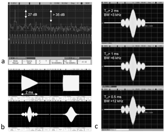
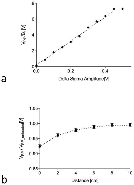
Figure 5(a) shows that attenuation of higher harmonics of the RF output signal was better than 27 dB. To analyze the performance of the AM system, different RF envelope shapes were encoded and the resulting modulated RF pulse was measured. Good performance of the envelope feedback in tracking the different wave profiles is shown in Fig. 5(b). High power bandwidths around 10 kHz were possible without any envelope correction as shown in Fig. 5(c). Additionally, Fig 6(a) shows that the output of the system measured as VPP/B1 increases linearly with the amplitude of the SDM encoded signal up to the saturation point of the PWM converter. This result confirmed the system’s static linearity that comes from the linear relationship that the PWM controller establishes between the amplitude of the target RF envelope and the actual measured output of the amplifier for a given feedback gain calibration. Even though the y-intercept was close to zero [Fig. 6(a)], RF leakage current was detected at the output stage during the cross-zero point of a sinc pulse of approximately 2.1% of the maximum peak of the RF envelope. This was reduced to less than 0.05% of the maximum amplitude by modulating the RF carrier around the zero crossings of the envelope, as detailed in the Material and Methods section, without distortion of the output signal (data not shown).
Figure 5.
Performance of the amplifier output filter. Frequency spectrum of RF output signal shows 3rd harmonic attenuation less than −25 dB (a). Four different types of modulated RF pulses (saw, square, sinc and gauss) measured by a pick-up loop coupled to the coil (b). Sinc pulses of increasing bandwidth and peak amplitude corresponding to approximately 3 A peak output current (c). No corrections to the RF envelope were performed in (b) and (c).
Figure 6.
Peak to peak voltage per B1 field (Vpp/B1) measured by a pick-up loop coupled to the coil while transmitting RF hard pulses of different amplitudes (a). Vpp/B1 normalized by the unloaded value vs. different load conditions set by varying the distance of a saline phantom to the coil (b).
The load sensitivity curve of the current mode amplifier is shown in Fig. 6(b). Here VPP/B1 was measured as the distance from the load to the coil was increased. Data were normalized by the VPP/B1 value corresponding to the unloaded condition. A maximum of 7% VPP/B1 variation was observed from the fully unloaded to the fully loaded condition, indicating a stable output largely independent of the loading.
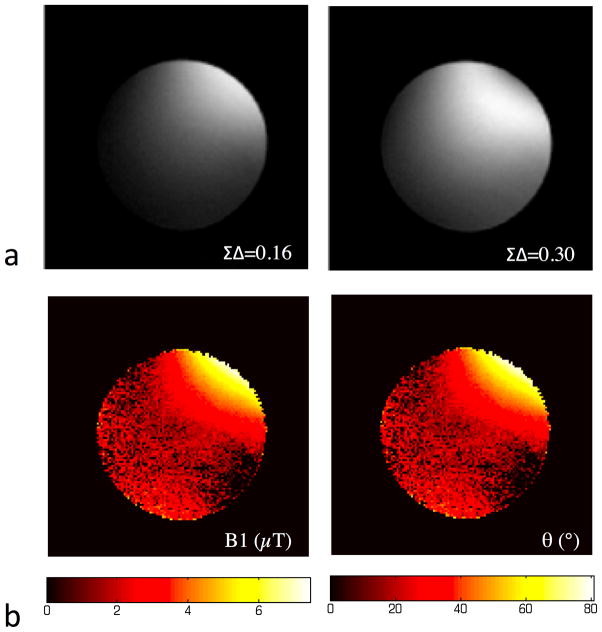
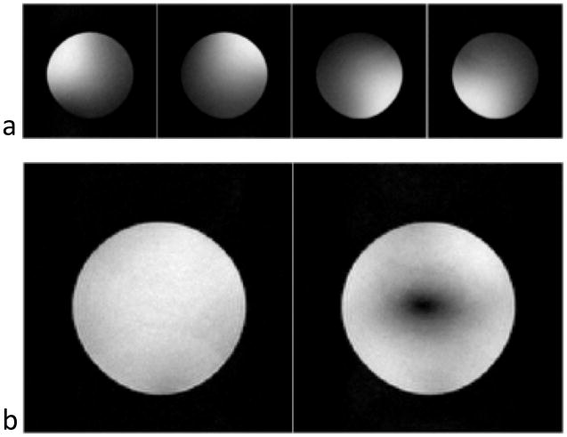
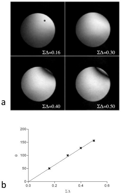
Figure 7(a) shows representative images (and value of the control variable) acquired for generation of the B1 maps. This high flip angle excitation resulted in well-defined B1 and flip angle mapping [Fig 7 (b)]. Images obtained with single-channel and simultaneous-channel transmission modes are shown in Fig. 8(a) and Fig. 8(b) respectively. During simultaneous transmission, phase of each channel was set such as to get a homogenous excitation mode (birdcage-like mode) and a gradient mode where the phase of successive channels was inverted and signal suppression at the center of the image was demonstrated as expected [Fig. 8(b)]. A similar experiment was performed for the two-coil setup that represents a harder condition for element decoupling due to the gapped neighboring coils located in planar configuration (Fig. 9). Successful decoupling is confirmed by images that result from single element transmission [Fig. 9(a)] and simultaneous transmission [Fig. 9(b)]. In this setup, due to the gap between coils, signal suppression in the center occurred for the in-phase transmission. Importantly, phase and amplitude for all the imaging experiments were set based on previous amplitude and phase benchtop calibrations and there were no interaction among elements that required iterations of these parameter values. Figure 10 (a) shows images acquired by transmitting with a single channel of the cylindrical array at different flip angles without any adjustment other than setting different values of the encoded sigma delta amplitude through the controller. Signal inversion was shifted toward the center of the phantom with increasing envelope amplitude. Flip angle maps were acquired for each condition, and flip angle value versus control signal amplitude for a marked region (square) is shown in Fig. 10 (b).
Figure 7.
Single channel images obtained by setting arbitrarily a current level at the amplifier output through the encoded control variable amplitude ΣΔ and by doubling the resulting current level (a). B1 map (in μT) and flip angle map (in degrees) (b), obtained by DAM through same GRE sequence used to acquire single channel images but at increased TR of 3s.
Figure 8.
Images of a saline phantom obtained by transmitting with the TX array and receiving with body coil. Images obtained by single channel transmission (a) and; birdcage and gradient mode images obtained with simultaneous transmission (b).
Figure 9.
Images obtained with the two-coil setup with 4 cm gap as it was set in benchtop decoupling measurements [Fig 3(b)]. Single channel transmission as performed in the cylindrical array (a) and simultaneous in-phase and 180 degree out-of phase transmission (b).
Figure 10.
Single channel transmission at different flip angles by direct control of the encoded envelope signal (ΣΔ) during same imaging experiment (a). Flip angle values at the highlighted pixel (white square) estimated from B1 maps (b).
Discussion
We have shown here a complete high efficiency transmit amplifier designed to be implemented in on-coil (or near-to-coil) transmit arrays. One of the key requirements for the design was to minimize power dissipation to make the system suitable for in-bore and/or on-coil amplification. Switch-mode amplifiers have a 100% theoretical efficiency and hence they are a better choice over linear amplifiers in terms of minimizing losses. Class-D amplification among other switch-mode configurations is a good trade-off between power efficiency and output distortion and it allows higher power levels [24]. We chose CMCD because it is relatively easy to build and tune for this application, while allowing for direct control of the B1 field which makes the system almost insensitive to loading and tuning. In our experiments, only a 7% variation was observed from fully unloaded to having the phantom in contact with the transmitting coil. Because of this, re-tuning of the coils was not necessary in any of the experiments carried out on the benchtop or in the scanner, since a spacing of 1–2 cm is almost always desirable in most imaging situations. These results show that recalibration of an array driven by CMCD amplifiers is unnecessary under a change in loading conditions which should provide a practical benefit in terms of setup time in the scanner.
We have also shown the driver system for switching the MOSFETs in the CMCD stage, where the key element was the class-D preamplifier. Using this type of preamplification, a high amplitude 180 degree out-of-phase voltage and enough output current was generated to drive the gate of the RF MOSFETs at minimum DC losses. The latter is important to keep the high intrinsic power efficiency of the CMCD stage which is not possible with linear preamplifier configurations [34]. Following this high power efficiency requirement, a switch-mode Buck converter with current feedback was designed to add the RF envelope information to the system. The system was able to track different RF envelopes of high amplitude and bandwidth. The static linearity between the B1 field amplitude and the control variable (amplitude of the SDM encoded envelope) was shown in the benchtop and in the scanner for two different gain calibrations, which is key for the effective control of the transmit field. It is clear that further corrections for some of the non-idealities of the output MOSFET in the encoding process are possible, such as the correction of RF-leakage currents due to the Cgd capacitance of the power MOSFET and potentially the compensation of phase modulation due to the effect of the drain-source capacitance.
As opposed to a standard 50 Ω amplifier system, power and efficiency measurement for the CMCD are not easy to perform. As presented in Materials and Methods section, in order to perform the measurements, the coil was replaced by the primary load of an impedance transformer built on a toroidal ferrite core whose secondary impedance was connected to 50 Ω power measurement setup. It should be noted that designing a transformer that down-converts this resistance to a few ohms in the MHz range with low insertion losses is not trivial. After previous attempts to measure output power with lower primary impedance (around 2 Ω) we set its value to approximately 7 Ω to minimize losses introduced by the transformer and cables used in this setup. Note that in both cases the effect of the MOSFET losses should be negligible with RDS at least 20 times lower than any of these primary impedance values. Power capability and efficiency values obtained in this setup were close to expected values. From previous attempts, we observed that the transformer setup could affect the performance of the amplifier by introducing conductive losses and increasing harmonic distortion. Increased THD at high power levels can occur due to the saturation of the ferrite of the impedance transformer that otherwise at lower power levels offers dramatic harmonic attenuation versus the air core transformer. For the presented setup, copper losses introduced by the transformer winding were minimized by increasing the wire cross-sectional area and reducing the number of primary and secondary turns for the required turn ratio, and THD was below 8 % for all power levels tested here. Since we measured amplifier output power indirectly by measuring the RMS voltage at the resonant operating frequency, reduction of higher harmonic distortion was important to avoid important underestimation of the output power level. As mentioned in the results section, the average drain efficiency of the CMCD was close to 81 % as estimated from power measurements performed with the transformer setup. The average buck converter efficiency was estimated above 75% and up to 93 % for different boards during RF transmission (data not shown here). For these estimates, input power measurements were strongly affected by RF noise due to the proximity of the input side of the converter board to the RF output stage, and efficiency estimates were only possible at input current levels above 1 A (above 200 mV voltage drop in a 0.2 Ω resistor).
Less than 10 °C temperature increment was measured when driving the transmitter continuously with same RF pulse and same duty cycle as in the performed imaging experiment and at the power setting corresponding to approximately 18 μT at the center of the coil as estimated from previously acquired B1 maps. This was achieved without the need of using a heatsink or forced air system as in the case of other current mode amplifier configurations [21]. In the performed experiments any heating of the electronics was dissipated only passively through the amplifier PC board. By avoiding the use of heatsinks the amplifier’s dimensions can be reduced, which may be beneficial since scalability will be important whenever one aims to implement a high number of elements. As expected, we measured higher increment of temperatures when testing the amplifier at more extreme operating conditions by setting duty cycles up to 50%. If the system is intended for use at higher duty cycles (usually not higher than 20–30% due to gradient limitations) and high flip angle excitations then heat dissipation could be further reduced by optimization of the power MOSFET’s PCB footprint and/or with the addition of small heat sinks locally attached to the MOSFET’s case such that thermal resistance is reduced.
Decoupling of elements during simultaneous and single channel transmission was achieved exclusively by amplifier decoupling. After testing different resonance conditions of the output filter on the benchtop and in the scanner, we found that no interaction among elements was observable when transmitting high power levels at decoupling values of 20 dB or higher. This is in agreement with other transmit setups already presented in the literature [35, 36]. Obtaining this decoupling condition across the whole operating drain voltage range was not possible in this configuration for a single value of Lf due to the large modulation of Cds value with drain voltage (from approximately 1000pF to 100 pF). We optimized decoupling at high voltage by maximizing the amplifier output impedance at approximately 15 V, at this condition, decoupling bencthop measurements confirmed by imaging experiments indicated decoupling better than 20 dB for VDD > 5 V. Note that the modulation effect on decoupling values caused by Cds will require further analysis if one is interested in simultaneous transmission of different pulse shapes, a situation that could be possible in more advanced parallel transmission applications. In the case of transmission with a subset of the available channels shown here, the inactive amplifiers were slightly biased at the drain to keep similar condition for the filter and decoupling values. In the presented experiment we used a jumper to the triggered +5 V line, even though this could also be performed automatically by modifying the AM board such that the voltage bias at the MOSFET drains never goes below a certain level, with the remaining modulation applied only to the RF input. This would require a more complicated, but not unrealistic, AM system than shown here.
As mentioned in the theory section, the output parallel resonant circuit filters out high harmonics from the load. We did not observe impact on THD when the filter was shifted from its ideal resonance condition (set at VDD = 15 V), as for example at high VDD. Note that the coil series resonance at 63.66 MHz acts as a filter itself and compensate for this non-ideality. It should be noted that the short cables used to connect the amplifier to the coil were effectively included in this filter circuit. These cables are not needed in general, but were used here to avoid susceptibility artifacts stemming from the metallic cases of the output MOSFETs used here. At the time of the construction of this array, the MRF275 was viewed as the ideal choice for the electrical performance of this amplifier. However, these cables could be eliminated if a suitable output FET could be found, and this is the subject of ongoing research in our group.
As mentioned before, the modulation of MOSFET’s output capacitance with drain voltage also produces a modulation of the RF phase. Even though this is non-ideal, we showed that this change in phase can be fully characterized and we believe it can be fully corrected at the time of encoding the RF carrier. In the presented experiments we were able to successfully drive both a birdcage-mode and a gradient-mode without any additional phase correction. Fundamentally, this VDD modulation’s effect will be intrinsically reduced when going to higher number of elements, since each element will have a lower power requirement, which will allow the use of MOSFETs with lower power ratings and thus lower junction capacitor values with lower modulation range (ΔCds).
As mentioned in the Materials and Method section, we used a DTG to synthesize all signals that drive the amplifier on the array. In this setup, data was programmed off-line in MATLAB using the SDM toolbox. Programming time as well as data uploading time to the synthesizer was dramatically increased when increasing number of channels and/or pulse length (e.g. programming time was approximately three times higher when going from one channel to 4 channels controlled independently). Thus, the DTG should be thought as a temporary device that worked well for running simple imaging sequences and few channels but it is clear that this device is not ideal. A dedicated hardware driver needs to be designed to run higher number of channels without a high penalty on the time of the experiment as well as to have higher integration of the system with the scanner and then reduce complexity of the control. With this setup, we were able to demonstrate simultaneous transmission without artifacts, confirming effective amplifier decoupling among elements and no interactions among amplifiers as predicted from measurements performed on the benchtop.
Conclusion
We have shown here a new approach to the design of multi-channel transmitter systems. Local power efficient transmission was possible through the design of class-D amplification and pre-amplification. Load insensitive operation was achieved through current mode operation of the amplifier output stage and feedback of the RF field envelope. Digitalization and optical transmission of the amplifier input signals eliminated the problem of cable coupling simplifying the configuration of the array by avoiding coaxial cable traps and reducing mechanical stress. Single and multiple channel transmission was successfully demonstrated in the scanner with direct control and quantification of the transmit field as indicated by the B1 maps. We believe the presented transmit system has a high potential in the implementation of large multiple-channel transmit arrays in an efficient and cost-effective way.
Acknowledgments
This research was supported by Siemens Medical Solutions. The authors would like to thank Colin Blumenthal and Lisa Bauer for their help on this project; the research groups at NHLBI and NINDS (National Institute of Health, Bethesda) for their support, especially to Michael Hansen, Helmut Merkle, Joe Murphy-Boesch and Stephen Dodd. The authors also want to acknowledge the anonymous reviewers for their comments that helped to improve this work.
References
- 1.Sotgiu A, Hyde JS. High-order coils as transmitters for NMR imaging. Magn Reson Med. 1986;3(1):55–62. doi: 10.1002/mrm.1910030108. [DOI] [PubMed] [Google Scholar]
- 2.Katscher U, Börnert P, Leussler C, van den Brink JS. Transmit SENSE. Magn Reson Med. 2003;49(1):144–150. doi: 10.1002/mrm.10353. [DOI] [PubMed] [Google Scholar]
- 3.Van de Moortele PF, Akgun C, Adriany G, Moeller S, Ritter J, Collins CM, Smith MB, Vaughan JT, Uğurbil K. B(1) destructive interferences and spatial phase patterns at 7 T with a head transceiver array coil. Magn Reson Med. 2005;54(6):1503–1518. doi: 10.1002/mrm.20708. [DOI] [PubMed] [Google Scholar]
- 4.Mao W, Smith MB, Collins CM. Exploring the limits of RF shimming for high-field MRI of the human head. Magn Reson Med. 2006;56(4):918–922. doi: 10.1002/mrm.21013. [DOI] [PMC free article] [PubMed] [Google Scholar]
- 5.Zhang Z, Yip C-Y, Grissom W, Noll DC, Boada FE, Stenger VA. Reduction of transmitter B1 inhomogeneity with transmit SENSE slice-select pulses. Magn Reson Med. 2007;57(5):842–847. doi: 10.1002/mrm.21221. [DOI] [PMC free article] [PubMed] [Google Scholar]
- 6.Graesslin I, Niemann M, Harvey P, Vernickel P, Katscher U. SAR and RF Power Reduction with Parallel Excitation using Non-Cartesian Trajectories. MAGMA. 2005;18:S251. [Google Scholar]
- 7.Lattanzi R, Sodickson DK, Grant AK, Zhu Y. Electrodynamic constraints on homogeneity and radiofrequency power deposition in multiple coil excitations. Magn Reson Med. 2009;61(2):315–334. doi: 10.1002/mrm.21782. [DOI] [PMC free article] [PubMed] [Google Scholar]
- 8.Wu X, Akgun C, Vaughan JT, Ugurbil K, Van de Moortele PF. SAR Reduction in Transmit SENSE Using Adapted Excitation K-Space Trajectories. Proceedings of the 15th ISMRM; Berlin, Germany. 2007; Abstract 673. [Google Scholar]
- 9.Zhu Y. Parallel excitation with an array of transmit coils. Magn Reson Med. 2004;51(4):775–784. doi: 10.1002/mrm.20011. [DOI] [PubMed] [Google Scholar]
- 10.Setsompop K, Alagappan V, Gagoski B, Witzel T, Polimeni J, Potthast A, Hebrank F, Fontius U, Schmitt F, Wald LL, Adalsteinsson E. Slice-selective RF pulses for in vivo B1+ inhomogeneity mitigation at 7 tesla using parallel RF excitation with a 16-element coil. Magn Reson Med. 2008;60(6):1422–1432. doi: 10.1002/mrm.21739. [DOI] [PMC free article] [PubMed] [Google Scholar]
- 11.Heilman JA, Derakhshan JJ, Riffe MJ, Gudino N, Tkach J, Flask CA, Duerk JL, Griswold MA. Parallel excitation for B-field insensitive fat-saturation preparation. Magn Reson Med. doi: 10.1002/mrm.23238. [DOI] [PMC free article] [PubMed] [Google Scholar]
- 12.Nielsen JF, Yoon D, Noll DC. Suppression of Banding and Transient Signal Oscillations in Balanced SSFP Using a Spoiled RF Pre-Phasing Approach. Proceedings of the 18th ISMRM; Stockholm, Sweden. 2010; Abstract 77. [Google Scholar]
- 13.Adriany G, Van de Moortele PF, Ritter J, Moeller S, Auerbach EJ, Akgün C, Snyder CJ, Vaughan T, Uğurbil K. A geometrically adjustable 16-channel transmit/receive transmission line array for improved RF efficiency and parallel imaging performance at 7 Tesla. Magn Reson Med. 2008;59(3):590–597. doi: 10.1002/mrm.21488. [DOI] [PubMed] [Google Scholar]
- 14.Adriany G, Auerbach EJ, Snyder CJ, Gözübüyük A, Moeller S, Ritter J, Van de Moortele PF, Vaughan T, Uğurbil K. A 32-channel lattice transmission line array for parallel transmit and receive MRI at 7 tesla. Magn Reson Med. 2010;63(6):1478–1485. doi: 10.1002/mrm.22413. [DOI] [PMC free article] [PubMed] [Google Scholar]
- 15.Hoult DI, Kolansky G, Kripiakevich D, King SB. The NMR multi-transmit phased array: a Cartesian feedback approach. J Magn Reson. 2004;171(1):64–70. doi: 10.1016/j.jmr.2004.07.020. [DOI] [PubMed] [Google Scholar]
- 16.Heid O. United States Patent: 6683457 - Magnetic resonance resonator system with coil branches operable with a time-delay relative to each other. 2004. [Google Scholar]
- 17.Kurpad KN, Wright SM, Boskamp EB. RF current element design for independent control of current amplitude and phase in transmit phased arrays. Concepts in Magnetic Resonance Part B: Magnetic Resonance Engineering. 2006;29B(2):75–83. [Google Scholar]
- 18.Heilman JA, Riffe MJ, Heid O, Griswold MA. High Power, High Efficiency On-Coil current mode amplifier for Parallel Transmission Arrays. Proceedings of the 15th ISMRM; Berlin, Germany. 2007; Abstract 171. [Google Scholar]
- 19.Scott GC, Stang P, Kerr A, Pauly J. General Signal Vector Decoupling for Transmit Arrays. Proceedings of the 16th ISMRM; Toronto, Canada. 2008; Abstract 146. [Google Scholar]
- 20.Chu X, Yang X, Liu Y, Sabate J, Zhu Y. ultra-low output impedance rf power amplifier for parallel excitation. Magn Reson Med. 2009;61(4):952–961. doi: 10.1002/mrm.21908. [DOI] [PMC free article] [PubMed] [Google Scholar]
- 21.Lee W, Boskamp E, Grist T, Kurpad K. Radiofrequency current source (RFCS) drive and decoupling technique for parallel transmit arrays using a high-power metal oxide semiconductor field-effect transistor (MOSFET) Magn Reson Med. 2009;62(1):218–228. doi: 10.1002/mrm.21988. [DOI] [PubMed] [Google Scholar]
- 22.Zanchi MG, Stang P, Kerr A, Pauly JM, Scott GC. Frequency-offset Cartesian feedback for MRI power amplifier linearization. IEEE Trans Med Imaging. 2011;30(2):512–522. doi: 10.1109/TMI.2010.2087768. [DOI] [PMC free article] [PubMed] [Google Scholar]
- 23.Roemer PB, Edelstein WA, Hayes CE, Souza SP, Mueller OM. The NMR phased array. Magn Reson Med. 1990;16(2):192–225. doi: 10.1002/mrm.1910160203. [DOI] [PubMed] [Google Scholar]
- 24.Kobayashi H, Hinrichs JM, Asbeck PM. Current-Mode Class-D Power Amplifiers for High-Efficiency RF Applications. IEEE Trans on Microwave Theory and Techniques. 2001;49(12) [Google Scholar]
- 25.Long A, Jingshi Yao, Long SI. Circuits and Systems. Vol. 1 MWSCAS; 2002. A 13 W current mode class D high efficiency 1 GHz power amplifier; p. I-33-6. [Google Scholar]
- 26.Kim Ji-Yeon, Han Dong-Hoon, Kim Jong-Heon, Stapleton SP. A 50 W LDMOS current mode 1800 MHz class-D power amplifier. Microwave Symposium Digest, IEEE MTT-S International; 2005. [Google Scholar]
- 27.Gudino N, Riffe MJ, Bauer LM, Heilman JA, Griswold MA. 1.5T On-Coil Current-Mode Class-D (CMCD) Amplifier with Amplitude Modulation Feedback and Voltage-Mode Class-D (VMCD) Preamplifier. Proceedings of the 18th ISMRM; Stockholm, Sweden. 2010; Abstract 43. [Google Scholar]
- 28.Kahn LR. Single sideband transmission by envelope elimination and restoration. Proc IRE. 1952;40:803–806. [Google Scholar]
- 29.Billings KH. Switchmode power supply handbook. New York: McGraw-Hill Professional; 1999. [Google Scholar]
- 30.Gudino N, Heilman JA, Griswold MA. High-Bandwidth, High-Efficiency RF Amplitude Modulation for On-Board Transmit Amplifiers. Proceedings of the 17th ISMRM; Hawaii, USA. 2009; Abstract 4769. [Google Scholar]
- 31.Heilman JA, Gudino N, Riffe MJ, Liu P, Griswold MA. A four channel transmission array based on CMCD amplifier. Proceedings of the 17th ISMRM; Hawaii, USA. 2009; Abstract 3027. [Google Scholar]
- 32.Candy JC, Temes G. Oversampling Delta-Sigma Data Converters: Theory, Design and Simulations. New York NY: IEEE Press; 1992. [Google Scholar]
- 33.Insko EK, Bolinger L. Mapping of the Radiofrequency Field. J Magn Reson, Series A. 1993;103(1):82–85. [Google Scholar]
- 34.Gudino N, Heilman JA, Riffe MJ, Flask CA, Griswold MA. 7T Current-Mode Class-D (CMCD) RF Power Amplifier. Proceedings of the 17th ISMRM; Hawaii, USA. 2009; Abstract 398. [Google Scholar]
- 35.Ullmann P, Junge S, Wick M, Seifert F, Ruhm W, Hennig J. Experimental analysis of parallel excitation using dedicated coil setups and simultaneous RF transmission on multiple channels. Magn Reson Med. 2005;54(4):994–1001. doi: 10.1002/mrm.20646. [DOI] [PubMed] [Google Scholar]
- 36.Vernickel P, Röschmann P, Findeklee C, Lüdeke KM, Leussler Ch, Overweg J, Katscher U, Grässlin I, Schünemann K. Eight-channel transmit/receive body MRI coil at 3T. Magn Reson Med. 2007;58(2):381–389. doi: 10.1002/mrm.21294. [DOI] [PubMed] [Google Scholar]


