Abstract
Graphene is a one atom thick carbon allotrope with all surface atoms that has attracted significant attention as a promising material as the conduction channel of a field-effect transistor and chemical field-effect transistor sensors. However, the zero bandgap of semimetal graphene still limits its application for these devices. In this work, ethanol-chemical vapor deposition (CVD) grown p-type semiconducting large-area monolayer graphene film was patterned into nanomesh by the combination of nanosphere lithography and reactive ion etching and evaluated as field-effect transistor and chemiresistor gas sensors. The resulting neck-width of the synthesized nanomesh was about ~20 nm comprised of the gap between polystyrene spheres that was formed during the reactive ion etching process. The neck-width and the periodicities of the graphene nanomesh could be easily controlled depending the duration/power of RIE and the size of PS nanospheres. The fabricated GNM transistor device exhibited promising electronic properties featuring high drive current and ION/IOFF ratio of about 6, significantly higher than its film counterpart. Similarly, when applied as chemiresistor gas sensor at room temperature, the graphene nanomesh sensor showed excellent sensitivity towards NO2 and NH3, significantly higher than their film counterparts. The ethanol-based graphene nanomesh sensors exhibited sensitivities of about 4.32%/ppm in NO2 and 0.71%/ppm in NH3 with limit of detections of 15 ppb and 160 ppb, respectively. Our demonstrated studies on controlling the neck width of the nanomesh would lead to further improvement of graphene-based transistors and sensors.
Keywords: Chemical vapor deposition, Nanosphere lithography, Graphene nanomesh, Transistor, Sensor
INTRODUCTION
Nanostructured materials are promising candidates as sensor elements due to their high surface-to-volume ratio that potentially leads to exceptional device performance, reduced device size and low power consumption1-4. Chemiresistor and field-effect transistors based sensors are the most common type and simplest sensors. In these types of sensors, the modulation of electrical resistance/conductance of the sensing element resulting from the interaction with the analyte is measured using a simple ohmmeter. Graphene, a one atom thick sp2 hybridized two-dimensional honeycomb lattice of carbon with extraordinary mechanical, thermal and electronic properties is an interesting nanomaterial that is receiving significant attention for chemiresistor (CR) and field-effect-transistor (FET) sensor devices5-8. Recently, there have been several reports in the literature demonstrating application of graphene for CR/FET chemical and biological sensors9,10. However, the material used, in all but one of the reported devices was chemically derived graphene, i.e. graphene oxide (GO). Although elegant, there are significant drawbacks in full-scale development of devices made from derived graphene/GO. First, GO is inherently insulating and hence it has to be reduced before it is useful as the conduction channel of CR/FET. Second, because of variability in the degree of reduction of the GO making the conduction channel of CR/FET there could be a problem in device-to-device reproducibility. Third, the expansion/exfoliation method used for producing GO produces micron size multilayer flakes of random geometry, which while suitable for single device fabrication for demonstration purposes, have serious limitations in fabrication of large numbers of devices with reproducible performance. These drawbacks can be alleviated using graphene or derivatized graphene with uniform morphological, chemical and electrical properties. This can be achieved by synthesizing graphene at wafer level using chemical vapor deposition. However, CVD produced graphene although provides patterning feasibility has zero bandgap, and FET devices made with such graphene cannot be truly turned off and hence cannot compete with conventional complementary metal-oxide-semiconductor (CMOS) devices in terms of ION/IOFF ratio. Recently, it has been shown theoretically and experimentally that lateral confinement of the graphene into sub-10 nm wide graphene nanoribbons (GNRs) could induce a bandgap by the quantum confinement and edge effects11.The bandgap of a GNR is related with the ribbon width by the equation: Eg = 0.8/W, where Eg is the bandgap and W is the ribbon width in nanometer12. Several reports have been published over the past few years showing the ability of bandgap tuning of ultra-narrow GNRs and their possible applications in nanoelectronics13-17. However, single GNR devices usually show low drive currents or low transconductances. Further, despite the promising electronic properties, single GNR devices cannot be applied on the platform of scalable electronics because there is no state-in-the-art technique to integrate them in a wafer scale circuitry. Moreover, patterning of wafer scale chemical vapor deposition (CVD)-grown graphene into sub-10 nm dimensions is still challenging with the e-beam lithography.
Recently, an approach named block copolymer lithography was reported to pattern micron-size exfoliated graphene into graphene nanomesh (GNM)18. The resulting GNMs exhibited large enough bandgap to be used as a semiconducting channel in a FET. In fact, GNM-FET devices showed reasonable ION/IOFF ratio with remarkably higher driving currents than single GNR-FET devices. The narrow neck-width of GNM confines the charge while being used as channel in an FET device. However, the size of the synthesized GNM by this method is limited to the micron-sized exfoliated graphene. Thus, synthesis of large area graphene nanomesh needs to be demonstrated using the state-of-art techniques to achieve larger device density for realizing its practical applications.
Previously, we showed that ethanol-based CVD grown graphene (gEtOH) exhibited a p-type semiconducting behavior due to the polycrystalline nature as opposed to the ambipolar electron transfer characteristics of methane-based CVD grown graphene (gCH4)19-21. In the two-dimensional (2D) polycrystalline gEtOH, grain boundaries are the one-dimensional (1D) interfaces between two crystalline domains with different crystallographic orientations. In fact, the grain boundaries and oxygenated functional groups present in the polycrystalline gEtOH act as defect sites to induce short-range charge disorder leading to higher ION/IOFF ratio in a gEtOH FET device21.
In this work, we report large area patterning of graphene film into GNM using a simple reactive-ion-etching (RIE) modified polystyrene (PS)-nanospheres-lithography technique. Using this approach the neck width of nanoporous mask can be tuned over a large range to finally achieve GNM with desired neck width. This approach can also be employed in fabricating large area nanomesh of different thin film semiconductors for nanoelectronics. The fabricated GNM devices were applied as gas sensors for toxic gases NO2 and NH3 that affect human health. We also fabricated sensor devices using graphene films to compare their sensitivity to nanomesh counterparts. Sensors fabricated from gEtOH nanomesh showed room temperature detection down to 15 ppb and 160 ppb of NO2 and NH3, significantly lower than Occupational Safety and Health Administration (OSHA) permissible exposure limits of 5 ppm (NO2) and 50 ppm (NH3), respectively.
METHODS
Growth of large area monolayer graphene film and patterning into graphene nanomesh (GNM)
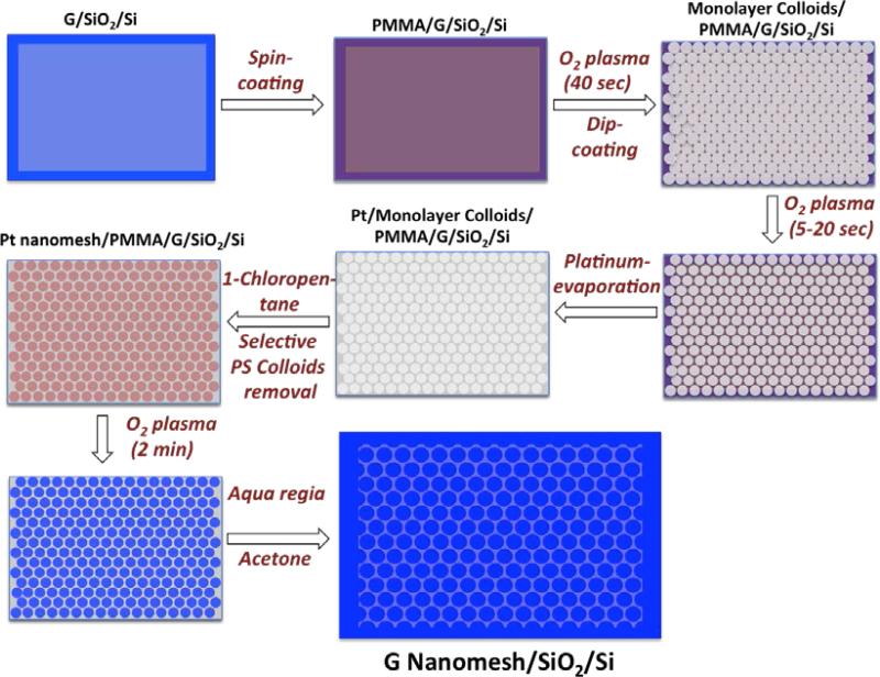
Large area (~1 in2) monolayer graphene films grown by methane-CVD and ethanol-CVD processes were transferred onto SiO2/Si substrate as reported previously.19-21 PMMA was spin-coated over the graphene/SiO2/Si substrates and baked at 110°C for 5min, followed by O2 plasma etching for 40 sec to make the surface hydrophilic. A stock solution consist of 10 wt% PS nanospheres (200 nm average diameter; Alfa Aesar) was ultra-sonicated in ethanol/water (1:1) solution for 30 min to disperse the PS nanospheres properly. A few drops of the stock solution were added on the D.I. water surface in a petri dish. In this step, several islands of monolayer PS nanospheres were visible on the water surface (Supplementary Fig. S1a). Interestingly, a drop of SDS (1%) solution immediately assembled those islands into a large area compact monolayer film of PS nanospheres on the water surface (Supplementary Fig. S1b). The PMMA coated graphene/SiO2/Si substrate was then brought into the contact of PS monolayer film on the water surface and easily transferred to cover the whole substrate, followed by drying in room temperature. Reactive ion etching (RIE; O2) was then employed at 75 W for 10 sec in flowing 50 sccm O2 to define 15-20 nm gap (comprised of resulting neck width of GNMs) between the nanospheres. A 15 nm Pt was deposited over the substrate using an e-beam evaporator (Temescal, BJD-1800) to fill up the gaps. A lift-off in 1-choropentane (Sigma-Aldrich) at 60°C for 2 h confirmed selective and complete removal of the PS nanosphere to result a perfect Pt nanomesh mask. In the second RIE step, the substrate was exposed to O2 plasma at 75 W for 150 sec in flowing 50 sccm O2 to remove the PMMA/graphene in the unprotected areas from Pt nanomesh. A second lift-off was carried out in acetone removed Pt nanomesh mask and PMMA to form GNM over SiO2/Si substrate.
Gas sensing measurements of GNMs sensor
GNMs sensor devices were fabricated by writing finger-like source-drain Ti (20 nm)/Au (180 nm) electrodes with 3 μm channel length defined by optical lithography. The samples were then mounted on a chip holder and wire bonded to complete fabrication of GNM chemiresistor gas sensor devices. GNM sensors were then placed inside 1.3 cm3 glass chamber with inlet and outlet ports. Dry air or air/NO2mixtures or air/NH3 mixtures was supplied into the glass chamber maintaining a total flow rate of 200 sccm controlled by mass flow controllers (MFCs). The sensor arrangement was subjected to 1 V source-drain (Vsd) bias and the two-probe resistance across the sensor was recorded continuously using a dual channel Keithley Source Meter (Model 2363A). A custom Labview program was developed to control the MFCs and monitor the resistance of the GNMs sensor devices. The sensor device was first purged with dry air for 200 min until the resistance of the sensors stabilized, followed by increasing NO2 or NH3 concentration in dry air every 15 min with an interval of 20 min recovery in air between two NO2 or NH3 exposures.
RESULTS AND DISCUSSION
Synthesis of large area GNM
Scheme 1 presents the detailed process flow for the synthesis of GNM from CVD-grown large area graphene film. The realization of a nanoporous mask of Pt over the large area graphene film which can then be exposed to O2 plasma to etch the graphene in the unprotected areas is the crucial step in synthesizing GNMs. The preparation of the Pt nanoporous mask consisted of four steps: 1) formation of a densely packed monolayer of PS nanospheres, 2) controlled etching of PS nanospheres to open gaps, 3) deposition of Pt and 4) removal of PS nanospheres. To form the densely packed monolayer of PS nanospheres on graphene/SiO2/Si substrate, PS nanospheres from a stock solution were spread on deionized (D.I.) water surface to form a large-area compact monolayer film of PS nanosphere on water surface (Supplementary Fig. S1). The total area of the assembled compact monolayer PS spheres can be readily increased depending on the area of water surface and the amount of PS stock solution. The PS nanospheres monolayer film was transferred onto PMMA coated graphene/SiO2/Si substrate by contacting the substrate with the PS nanospheres monolayer film floating on water followed by drying the substrate in room temperature.
Scheme 1.
Detailed process flow to synthesize large area GNM using PS nanosphere lithography.
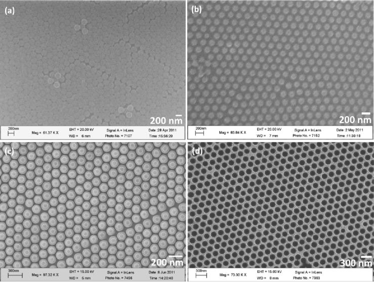
Figure 1 shows self-assembled monolayer of PS spheres transferred onto PMMA/graphene/SiO2/Si substrate. A monolayer of PS spheres (~200 nm) formed a close-packed hexagonal array over the entire substrate (Fig. 1a). The simple methodology of making closely packed nanospehere layer demonstrated here can be easily scaled to wafer level by using a larger water surface. PS nanospheres were then etched using RIE. This is an important step as it will determine the neck width of the final graphene nanomesh, a larger reduction in PS nanosphere size will produce a wider neck width and vice-versa (Supplementary Fig. S2). As shown in Figure 1b, RIE for 10 sec at 100W in flowing 50 sccm of flowing O2, reduced the PS nanosphere size to form an average gap of about ~20 nm while keeping the pitch between the PS spheres unchanged. However, almost all PS nanospheres were etched away leaving debris of small PS fragments when the etching time was increased to 20 s (Supplementary Fig. S2c). On the other hand, an etching time of 5 s did not produce sufficient etching to produce any gap (Supplementary Fig. S2a). Following the RIE, 15 nm thick Pt was deposited in the gap between PS nanospheres (Fig. 1c) by metal evaporator and the sample was processed to remove the PS nanospheres.
Figure 1. PS nanospheres assembling and Pt nanomesh formation.
SEM images of self-assembled monolayer of PS spheres onto PMMA/gEtOH/SiO2/Si substrate a, before and b, after 10 s RIE etching. c,15 nm Pt deposited over the substrate in (b) to fill up the gaps between the PS spheres. d, Formation of Pt nanomesh mask onto PMMA/gEtOH/SiO2/Si substrate by removal of PS spheres in 1-chloropentane.
The complete removal of PS nanospheres is another critical step in the production of a perfect Pt nanomesh over the entire substrate. The existence of any PS nanosphere in the Pt nanomesh is problematic since the unremoved PS sphere would protect graphene from etching in O2 plasma, resulting in a defect in the nanoporous periodicity in the eventual GNM. Three different methods - ultrasonication, wet-etching (lift-off) and a combination of the two - were evaluated for PS nanosphere removal. Ultrasonication is the most commonly use method to remove colloidal spheres22. Ultrasonication intervals of 30, 60 and 90s for PS sphere removals were investigated and the SEM images of Pt nanomesh after removal of PS spheres are shown in Supplementary Figure S3. A 30 s ultrasonication was totally inefficient for the PS spheres removal (Supplementary Fig. S3a). Increasing the ultrasonication time to up to 90 s while removed PS spheres from some additional sections, most of the PS spheres still remained on the substrate (Supplementary Fig. S3c). A magnified image (Supplementary Figure S3d), taken from region P in Supplementary Fig. S3c, confirmed the Pt nanomesh in the areas where PS spheres were removed to be without damage and had certain periodicity. However, a longer sonication time disintegrated the Pt nanomesh (figure not shown).
Selective solvents have been used for reversible self-assembly or reconstruction/reorganization of polymer domains in block copolymers23,24. Cyclohexane has been recognized as one such solvent for selective removal of PS in PMMA matrix25. Figure Supplementary S4 shows SEM images of Pt deposited substrate after immersing in cyclohexane at 60°C for 2 h. As shown in the figure, some PS spheres were released or tended to release at some satellite areas but it did not remove all the spheres (Supplementary Fig. S4a). The primary result of the treatment was a decrease in the diameter of the PS spheres due to the surface etching with almost all spheres staying attached on the underneath PMMA surface (Supplementary Fig. S4a). This may be due to the residual PS remaining at the interface of PS spheres and PMMA surface, and the PS adsorbed to PMMA surface from solution of PS in cyclohexane26. Additional sonication of 90s after wet-etching had some success in removing PS from more areas, but once again there were still large patches/sections of unremoved PS spheres (Supplementary Fig. S4b).
To further investigate/optimize the conditions for the complete removal of PS spheres, 1-chloropentane was used as an alternative selective solvent and the results were compared with cyclohexane-treated samples (Supplementary Fig. S5). As shown in Figure S5b, 1-chloropentane treatment was significantly more efficient in removing PS spheres when compared to cyclohexane (Supplementary Fig. S5a). In fact, PS spheres were essentially non-existent in the Pt nanomesh after 1-chloropentane treatment, as a consequence of 1-chloropentane providing a weaker driving force than cyclohexane for adsorption of PS to PMMA26. This resulting material was treated with O2 plasma (100 W for 150 s in 50 sccm flowing O2 atmosphere) followed by lift-off in acetone to obtain the final GNM product.
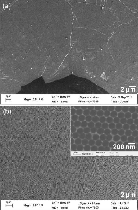
Figure 2 shows SEM images of (a) large area CVD-grown graphene and corresponding (b) GNM. As shown in the inset of Fig. 2b, the synthesized GNM exhibited narrow neck-width of about ~20 nm with certain periodicity. This process also demonstrated that large area GNMs with desired neck-widths and periodicities could be attained by changing the duration/power of RIE and the diameter of PS spheres (Supplementary Fig. S6). Several wrinkles were frequently observed in the large-area graphene film during the transfer process (Figure 2a). These wrinkles were either broken or remained during the nanomesh processing steps, and their traces are clearly visible in the large area nanomesh (Fig. 2b). However, our demonstrated processing steps on ultraflat graphene27 would potentially remove these defects over the entire GNM surface.
Figure 2. Morphology of synthesized large area GNM.
SEM images of a, large area CVD-grown gEtOH film onto SiO2/Si substrates and corresponding synthesized b, gEtOH nanomesh onto SiO2/Si substrate after etching of PMMA/gEtOH films in the unprotected areas, followed by removal of Pt nanomesh mask and PMMA using lift-off in acetone.
Transfer characteristics of GNM transistors
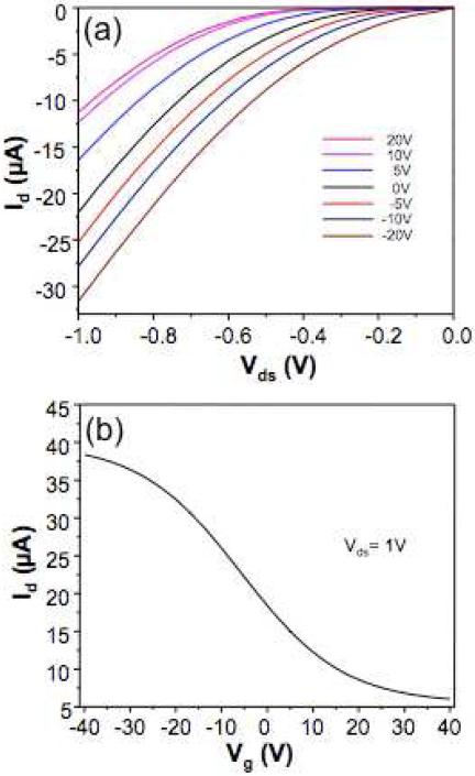
To investigate the electronic properties of fabricated GNM-based transistor, a three terminal transistor device was made using GNM as the semiconducting channel, e-beam evaporated Ti (20 nm)/Au (180 nm) as source-drain contacts, a highly doped p-type Si as global back gate, and 300 nm thermally grown SiO2 as the gate dielectric. Figure 3a shows the electrical transfer characteristics of the fabricated GNM transistor with a neck-width ~20 nm. As illustrated in the figure, the GNM exhibited p-type transistor behavior (Fig. 3a). The hole-doping of synthesized GNM can be attributed to the edge oxidation during the O2 plasma process, similar to the GNR-based transistor devices reported earlier12. The Id-Vg curve (Fig. 3b) at a Vsd of 1 V showed the GNM device to have an ION/IOFF ratio of ~6.5, which is higher than the ethanol-based graphene film (~ 3)21, and comparable to sub-20nm width GNR transistor device (~ 5)12. Further optimization of RIE conditions should easily allow synthesizing GNM with narrower necks (Supplementary Fig. S6), thus providing higher ION/IOFF GNM transistor devices.
Figure 3. Transfer characteristics of synthesized GNM film (Lc=3 μm and Wc=200 μm).
a) Low bias two terminal source–drain current (Id) as function of source-drain voltage (Vds) at constant gate potential (Vg) and b) source-drain current (Id) as a function of gate potential (Vg) at constant Vds of 1V.
Gas sensing properties of GNM sensors
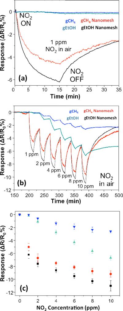
To evaluate the application of GNM for chemiresistor sensors, gEtOH and gCH4 nanomesh were applied as conduction channel between a pair of photolithographically defined Ti/Au electrodes, acting as source and drain, separated by a 3 μm gap. For comparison, sensor devices made of gEtOH and gCH4 film conduction channels were also evaluated. To start, the devices were tested for their response (normalized resistance change) to 1 ppm NO2. As illustrated in Fig. 4a, gEtOH nanomesh sensor exhibited the best response (~6%) followed by gCH4 nanomesh sensor (~4.5%) whereas there was no response from their film counterparts. The decrease in resistance of the device is attributed to increase in hole-density of p-type semiconductor graphene upon adsorption the electron acceptor NO2. The very good response from GNM devices compared to the film counterparts is attributed to the formation of large number of edges in the nanomesh structure that leads to hole doping by edge-oxidation during the O2 plasma process and/or physisorbed oxygen from the ambient and other species during the sample preparation steps similar to that of GNRs devices28,29. On the other hand, the narrow neck regions of GNM controls the charge transport across the source-drain electrodes by lateral quantum confinement, leading to higher sensitivity while being exposed to electron donating or withdrawing gas/bio molecules30.
Figure 4. Room temperature NO2 detection of GNM sensor.
a, Comparison of dynamic responses of sensor devices fabricated from gCH4 and gEtOH nanomesh and their continuous film counterparts to 1 ppm NO2 in dray air. b, Comparison of dynamic responses of sensor devices fabricated from gCH4 and gEtOH nanomesh and their continuous film counterparts exposed to various concentrations of NO2 in dry air ranging from 1 ppm to 10 ppm, as labeled. c, Calibration curves of gCH4 and gEtOH nanomesh sensor devices in various concentrations NO2 in dry air.
Figure 4b and 4c show the dynamic responses and calibration plots, respectively, of chemiresistor sensors made with gEtOH and gCH4 GNM and films as conduction channel operating at room temperature for increasing NO2 concentrations. Similar to response for 1 ppm NO2, the responses over the tested range of 1 to 10 ppm NO2 was in the order, gEtOH nanomesh > gCH4 nanomesh > gEtOH film > gCH4 film. Further, the response time, defined as the time required to reach a 90% of the maximum resistance change, for GNM sensors at 1 ppm NO2 in dry air was approximately 7 min and decreased to 5 min at 10 ppm. The slow response time is consistent with previous reports.31, 32 The relationship between the sensor response and concentration (Fig. 4c) exhibited the Langmuir-like absorption isotherm, where the relationship between the response and concentration is governed by the eqn.
where (ΔR / RO)max is the maximum change in normalized resistance occurring in the saturation regime, and k is the affinity constant. The sensitivity (slope of the linear part of calibration curve) and estimated limit of detection (defined as LOD=3SD/m, where m is the slope of linear part of the calibration curve and SD is the standard deviation of noise in the response curve in dry air) of the gEtOH nanomesh NO2 sensor were determined to be 4.32%/ppm and 15 ppb (parts-per-billion), respectively. This result is superior to the 3.5%/ppm sensitivity and 1 ppm LOD reported for three-dimensional CNTs (20μm)/reduced graphene hybrid NO2 sensor, and to the negligible to 0.6%/ppm sensitivity of reduced graphene oxide films31 and flakes32, respectively. Moreover, this result is also comparable to NO2 detection limits of 44 ppb of pristine SWNT33, ~5 ppb for gold functionalized SWNTs34 and 100 ppt of polyethyleneimine coated SWNTs35.
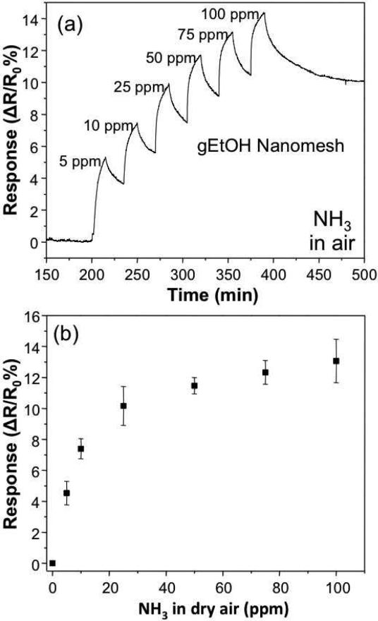
Furthermore, similar to the case of carbon nanotubes36,37, the resistance of the GNM sensor devices increased when exposed to NH3 (an electron donor), (Fig. 5a). This result suggests that the response of p-type gEtOH nanomesh sensor device to NH3 is due to the depletion of holes during the electron transfer from NH3 molecules to the nanomesh surface38,39. There was a monotonic increase in responses with the increasing NH3 concentrations ranging from 5 ppm to 100 ppm in dry air. The sensitivity and estimated LOD of gEtOH sensor devices calculated from the calibration curve in Figure 5b were about 0.71%/ppm and 160 ppb, respectively. This result is comparable to NH3 detection limits of 262 ppb of pristine SWNT33 and 50 ppb of functionalized SWNTs40.
Figure 5. Room temperature NH3 detection of GNM sensor.
a, Dynamic response and b, calibration curve of gEtOH nanomesh sensor device exposed to various concentrations of NH3 in dry air ranging from 5 ppm to 100 ppm, as labeled.
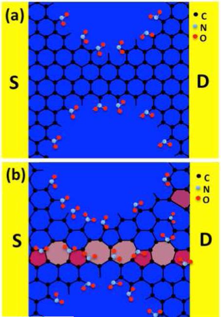
Graphene has similar graphitic structure as CNTs, and thus exhibit similar working principle of electrical conductivity modulation by the charge transfer mechanism in detecting gas molecules adsorbed at its surface. However, it has been recognized that pristine CNTs exhibit weak binding energies to the foreign molecules and thereby show poor reactivity at their defect-free surfaces due to small charge transfers from the adsorbed molecules. In fact, in our previous work we demonstrated that compared to CVD-synthesized gCH4 film, CVD-synthesized gEtOH film exhibits polycrystallinity containing highly disordered sp3 hybridization, large number of edge defects and oxygenated functional groups, affecting it's electronic and transport properties21. Figure 6 shows a schematic diagram (not to scale) comparing the structural differences between gCH4 and gEtOH nanomesh sensor devices. The gCH4 nanomesh contains defects mostly formed due to the formation the edges of nanoholes during nanosphere lithography (Fig. 6a), whereas gEtOH nanomesh had additional unsaturated grain boundary (intrinsic topological defect as labeled by colored pentagons and heptagons) due to its polycrystalline nature (Fig. 6b), which could modulate the charge transport properties41,42. Moreover, the higher defects density of the oxygenated gEtOH films could modify the local electronics-charge distribution, enhancing the reactivity at those specific sites43,44. These highly reactive defects of gEtOH film or nanomesh give rise to higher sensitivity by the adsorption of maximum number of NO2 molecules. This is also evident in the NO2 response curves of GNM devices. As shown in Figures 4a and 4b, both gEtOH and gCH4 nanomesh devices had almost similar response time but different response intensities. The gCH4 film/nanomesh had lesser defect sites than gEtOH film/nanomesh to have less number of NO2 molecules adsorb on the surface as shown in Figure 4, limiting the low conductivity modulation.
Figure 6. Crystal structures of gCH4 and gEtOH nanomeshes.
A structural representation (not to scale) comparing the defect densities between a, gCH4 and b, gEtOH nanomesh sensor devices, and adsorptions of NO2 molecules on the defect sites. A typical intrinsic defect (grain boundary) of polycrystalline gEtOH nanomesh labeled as colored unsaturated carbon (pentagons and heptagons) structure in b.
CONCLUSIONS
Using a simple polystyrene nanosphere lithography technique, we systemically investigated the process conditions and synthesized large-area graphene nanomesh from CVD-grown graphene film. In fact, this method can be scaled to wafer scale GNMs using the current wafer scale CVD grown graphene platform. The resulting neck-width of the synthesized nanomesh was about ~20 nm and comprised of the gap between polystyrene spheres that was formed during the reactive ion etching process. Fabricated graphene nanomesh sensor devices represented remarkably higher sensitivity to both NO2 and NH3 exposures than their film counterparts. Due to the higher defect density, ethanol-derived graphene nanomesh sensor showed enhanced responses and sensitivity than the methane-derived graphene nanomesh devices by the adsorption of maximum number of gas molecules. The sensitivity and estimated limit of detection of ethanol-based graphene nanomesh devices operating at room temperature were about 4.32%/ppm and 15 ppb in NO2, and 0.71%/ppm and 160 ppb in NH3, respectively. These results revealed that the fabricated GNM sensors could be successfully used for detection of other electron-donating or electron-withdrawing species. Further, the decrease in neck width of synthesized nanomesh and/or surface modification of those nanomesh sensor devices with polymers or catalyst nanoparticles would further increase the sensitivity and selectivity.45 Additionally, the excellent thermal properties of graphene will permit the application of this gas sensor for many high temperature sensing applications. Operating at higher temperature will improve the sensor response and recovery times and selectivity while lowering the sensitivity when compared to room temperature operation.46
Supplementary Material
ACKNOWLEDGEMENTS
We acknowledge the NIH grant U01ES016026, Nanosense Inc. and Bourns College of Engineering Dean for financial support and Mr. Edward DeLao for help with gas sensing experiments.
Contributor Information
Rajat Kanti Paul, Department of Mechanical Engineering, University of California, Riverside, CA 92521, USA.
Sushmee Badhulika, Department of Electrical Engineering, University of California, Riverside CA 92521, USA.
Nuvia M. Saucedo, Department of Chemistry, University of California, Riverside CA 92521, USA
Prof. Ashok Mulchandani, Department of Chemical and Environmental Engineering, University of California, Riverside CA 92521, USA.
REFERENCES
- 1.Xia YN, Yang PD, Sun YG, Wu YY, Mayers B, Gates B, Yin YD, Kim F, Yan YQ. Adv. Mater. 2003;15:353–389. [Google Scholar]
- 2.Johnson JL, Behnam A, Pearton SJ, Ural A. Adv. Mater. 2010;22:4877–4800. doi: 10.1002/adma.201001798. [DOI] [PubMed] [Google Scholar]
- 4.Paul RK, Badhulika S, Mulchandani A. Appl. Phys. Lett. 2011;99:033103–033105. [Google Scholar]
- 5.Novoselov KS, et al. Electric field effect in atomically thin carbon films. Science. 2004;306:666–669. doi: 10.1126/science.1102896. [DOI] [PubMed] [Google Scholar]
- 6.Frank IW, Tanenbaum DM, Van der Zande AM, McEuen PL. J. Vac. Sci. Technol. B. 2007;25:2558–2561. [Google Scholar]
- 7.Balandin AA, Ghosh S, Bao WZ, Calizo I, Teweldebrhan D, Miao F, Lau CN. Nano Lett. 2008;8:902–907. doi: 10.1021/nl0731872. [DOI] [PubMed] [Google Scholar]
- 8.Geim AK, Novoselov KS. Nat. Mater. 2007;6:183–191. doi: 10.1038/nmat1849. [DOI] [PubMed] [Google Scholar]
- 9.Lu G, Park S, Yu KH, Ruoff RS, Ocola LE, Rosenmann D, Chen JH. ACS Nano. 2011;5:1154–1164. doi: 10.1021/nn102803q. [DOI] [PubMed] [Google Scholar]
- 10.Kuila T, Bose S, Khanra P, Mishra AK, Kim NH, Lee JH. Biosensors and Bioelectronics. 2011;26:4637–4648. doi: 10.1016/j.bios.2011.05.039. [DOI] [PubMed] [Google Scholar]
- 11.Lam KT, Seah D, Chin SK, Kumar SB, Samudra G, Yeo YC, Liang G. IEEE Electron Device Lett. 2010;31:555–557. [Google Scholar]
- 12.Li X, Wang X, Zhang L, Lee S, Dai H. Science. 2008;319:1229–1232. doi: 10.1126/science.1150878. [DOI] [PubMed] [Google Scholar]
- 13.Ritter KA, Lyding JW. Nat. Mater. 2009;8:235–242. doi: 10.1038/nmat2378. [DOI] [PubMed] [Google Scholar]
- 14.Shimizu TS, Haruyama J, Marcano DC, Kosinkin DV, Tour JM, Hirose K, Suenaga K. Nat. Nanotechnol. 2011;6:45–50. doi: 10.1038/nnano.2010.249. [DOI] [PubMed] [Google Scholar]
- 15.Bai JW, Cheng R, Xiu FX, Liao L, Wang MS, Shailos A, Wang KL, Huang Y, Duan XF. Nat. Nanotechnol. 2010;5:655–659. doi: 10.1038/nnano.2010.154. [DOI] [PMC free article] [PubMed] [Google Scholar]
- 16.Jiao L, Wang X, Diankov G, Wang H, Dai H. Nat. Nanotechnol. 2010;5:321–325. doi: 10.1038/nnano.2010.54. [DOI] [PubMed] [Google Scholar]
- 17.Sprinkle M, Ruan M, Hu Y, Hankinson J, Rubio-Roy M, Zhang B, Wu X, Berger C, 2, de Heer WA. Nat. Nanotechnol. 2010;5:727–731. doi: 10.1038/nnano.2010.192. [DOI] [PubMed] [Google Scholar]
- 18.Bai J, Zhong X, Jiang S, Huang Y, Duan X. Nat. Nanotechnol. 2010;5:190–194. doi: 10.1038/nnano.2010.8. [DOI] [PMC free article] [PubMed] [Google Scholar]
- 19.Li XS, Cai WW, An JH, Kim S, Nah J, Yang DX, Piner R, Velamakanni A, Jung I, Tutuc E, Banerjee SK, Colombo L, Ruoff RS. Science. 2009;324:1312–1314. doi: 10.1126/science.1171245. [DOI] [PubMed] [Google Scholar]
- 20.Donga X, Wanga P, Fangc W, Sud CY, Chend YH, Lid LJ, Huanga W, Chen P. Carbon. 2011;49:3672–3678. [Google Scholar]
- 21.Paul RK, Badhulika S, Niyogi S, Haddon RC, Boddu VM, Costales-Nieves C, Bozhilov KN, Mulchandani A. Carbon. 2011;49:3789–3795. doi: 10.1016/j.carbon.2011.04.070. [DOI] [PMC free article] [PubMed] [Google Scholar]
- 22.Sinitskii A, Tour JM. J. Am. Chem. Soc. 2010;132:14730–14732. doi: 10.1021/ja105426h. [DOI] [PubMed] [Google Scholar]
- 23.Lin H, Steyerl A, Satija SK, Karim A, Russell TP. Macromolecules. 1995;28:1470–1474. [Google Scholar]
- 24.Xu T, Goldbach JT, Misner MJ, Kim S, Gibaud A, Gang O, Ocko B, Guarini KW, Black CT, Hawker CJ, Russell TP. Macromolecules. 2004;37:2972–2977. [Google Scholar]
- 25.García PD, Sapienza R, Blanco A, López C. Adv. Mater. 2007;19:2597–2602. [Google Scholar]
- 26.Harton SE, Luning J, Betz H, Ade H. Macromolecules. 2006;39:7729–7733. [Google Scholar]
- 27.Lui CH, Liu L, Mak KF, Flynn GW, Heinz TF. Nature. 2009;462:339–341. doi: 10.1038/nature08569. [DOI] [PubMed] [Google Scholar]
- 28.Li TC, Lu SP. Phys. Rev. B. 2008;77:085408–085415. [Google Scholar]
- 29.Sols F, Guinea F, Castro Neto AH. Phys. Rev. Lett. 2007;99:166803–166806. doi: 10.1103/PhysRevLett.99.166803. [DOI] [PubMed] [Google Scholar]
- 30.Schedin F, Geim AK, Morozov SV, Hill EW, Blake P, Katsnelson MI, Novoselov KS. Nat. Mater. 2007;6:652–655. doi: 10.1038/nmat1967. [DOI] [PubMed] [Google Scholar]
- 31.Jeong HY, Lee DS, Choi HK, Lee DH, Kim JE, Lee JY, Lee WJ, Kim SO, Choi SY. Appl. Phys. Lett. 2010;96:213105–213107. [Google Scholar]
- 32.Dua V, Surwade SP, Ammu S, Agnihotra SR, Jain S, Roberts KE, Park S, Ruoff RS, Manohar SK. Angew. Chem. Int. Ed. 2010;49:2154–2157. doi: 10.1002/anie.200905089. [DOI] [PubMed] [Google Scholar]
- 33.Li J, Lu Y, Ye Q, Cinke M, Han J, Meyyappan M. Nano Lett. 2003;3:929–933. [Google Scholar]
- 34.Young P, Lu YJ, Terrill R, Li JJ. Nanoscience and Nanotechnol. 2005;5:1509–1513. doi: 10.1166/jnn.2005.323. [DOI] [PubMed] [Google Scholar]
- 35.Qi P, Vermesh O, Grecu M, Javey A, Wang Q, Dai H. Nano Lett. 2003;3:347–351. doi: 10.1021/nl034010k. [DOI] [PubMed] [Google Scholar]
- 36.Collins PG, Bradley K, Ishigami M, Zettl A. Science. 2000;287:1801–1804. doi: 10.1126/science.287.5459.1801. [DOI] [PubMed] [Google Scholar]
- 37.Kong J, Franklin NR, Zhou CW, Chapline MG, Peng S, Cho KJ, Dai HJ. Science. 2000;287:622–625. doi: 10.1126/science.287.5453.622. [DOI] [PubMed] [Google Scholar]
- 38.Sundaram RS, Gomez-Navarro C, Balasubramanian K, Burghard M, Kern K. Adv. Mater. 2008;20:3050–3053. [Google Scholar]
- 39.Kong J, Chapline M, Dai H. Adv. Mater. 2001;13:1384–1386. [Google Scholar]
- 40.Zhang T, Nix MB, Yoo BY, Deshusses MA, Myung NV. Electroanalysis. 2006;18:1153–1158. [Google Scholar]
- 41.Kim P. Nat. Mater. 2010;9:792–793. doi: 10.1038/nmat2862. [DOI] [PubMed] [Google Scholar]
- 42.Yazyev OV, Louie SG. Nat. Mater. 2010;9:806. doi: 10.1038/nmat2830. [DOI] [PubMed] [Google Scholar]
- 43.Zanolli Z, Charlier JC. Phys. Rev. B. 2009;80:155447–155452. [Google Scholar]
- 44.Kudin KN, Ozbas B, Schniepp HC, Prud'homme RK, Aksay IA, Car R. Nano Lett. 2008;8:36–41. doi: 10.1021/nl071822y. [DOI] [PubMed] [Google Scholar]
- 45.Yavari F, Koratkar NJ. Phys. Chem. Lett. 2012;3:17461753. doi: 10.1021/jz300358t. [DOI] [PubMed] [Google Scholar]
- 46.Fowler JD, Allen MJ, Tung VC, Yang Y, Kaner RB, Weiller BH. ACS Nano. 3:301–306. doi: 10.1021/nn800593m. [DOI] [PubMed] [Google Scholar]
Associated Data
This section collects any data citations, data availability statements, or supplementary materials included in this article.


