Abstract
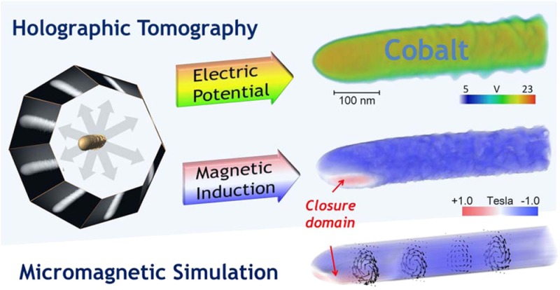
The investigation of three-dimensional (3D) ferromagnetic nanoscale materials constitutes one of the key research areas of the current magnetism roadmap and carries great potential to impact areas such as data storage, sensing, and biomagnetism. The properties of such nanostructures are closely connected with their 3D magnetic nanostructure, making their determination highly valuable. Up to now, quantitative 3D maps providing both the internal magnetic and electric configuration of the same specimen with high spatial resolution are missing. Here, we demonstrate the quantitative 3D reconstruction of the dominant axial component of the magnetic induction and electrostatic potential within a cobalt nanowire (NW) of 100 nm in diameter with spatial resolution below 10 nm by applying electron holographic tomography. The tomogram was obtained using a dedicated TEM sample holder for acquisition, in combination with advanced alignment and tomographic reconstruction routines. The powerful approach presented here is widely applicable to a broad range of 3D magnetic nanostructures and may trigger the progress of novel spintronic nonplanar nanodevices.
Introduction
A thorough understanding of the connection between the structure and the magnetic properties of nanostructures requires characterization techniques that permit direct measurements of magnetic ordering at the submicron scale. Therefore, together with the high control achieved for the growth of thin films during the last decades, there has been an increasing development of magnetic imaging techniques for two-dimensional ferromagnetic nanostructures. Along with the decrease of the computation time of micromagnetic simulations, these techniques have significantly contributed to deeper insights into nanoscale magnetic phenomena, thereby boosting the development of novel technological applications in the field of Nanomagnetism and Spintronics.1−5 Recently, a new possible route has been proposed in this area, based on the use of 3D magnetic nanostructures for their exploitation in data storage and logic.1,2,5 Moving toward spintronic architectures which go beyond a planar configuration not only requires nonstandard lithography techniques but also demands advanced imaging techniques that can resolve the magnetism of nanostructures in 3D.
Among various magnetic imaging techniques, such as Kerr microscopy, spin-polarized low-energy electron microscopy (SPLEEM), X-ray magnetic circular dichroism photoelectron emission microscopy (XMCD-PEEM), magnetic force microscopy (MFM), and spin-polarized scanning tunneling microscopy (SP-STM), off-axis electron holography (EH) is one of the most powerful methods to obtain quantitative measurements of local magnetization inside and around magnetic nanomaterials with nanometric resolution.6,7
EH is a transmission electron microscopy (TEM) technique that utilizes the interference of a split electron wave to measure the phase shift of one of the partial waves when interacting with an electrostatic and/or a magnetic field. Aharonov and Bohm8 have demonstrated that this phase shift between object wave and unperturbed reference wave can be expressed by the phase grating approximation (PGA), i.e.
| 1 |
where CE is an interaction constant depending on the electron beam energy, V(x,y,z) is the three-dimensional electrostatic object potential, e is the elementary charge, ℏ is the reduced Planck constant, and Az(x, y, z) is the component of the magnetic vector potential parallel to the electron beam direction z. Accordingly, the first term can be considered as electric phase shift φel and the second one as magnetic phase shift φmag. Consequently, the projections of the lateral components of the magnetic induction B = (Bx, By, Bz)T may be obtained by differentiating φmag according to
| 2 |
and
| 3 |
Owing to these relations EH can directly visualize the projected magnetic induction Bx,y in and around nanostructures,9,10 which was successfully exploited to investigate magnetic configurations in magnetotactic bacteria,11 Fe nanocubes,12 Ni nanowires,13 and other types of complex nanostructures such as magnetic tunnel junctions.14 However, a single EH experiment only permits recovering the magnetic field components integrated along the beam path through the sample.15 In order to obtain information about the 3D magnetic structure from such a 2D projection, additional input, e.g., from micromagnetic simulations, is required.
Combining EH with electron tomography to electron holographic tomography (EHT) can overcome this problem. EHT starts with acquiring a tilt series of electron holograms from the same nanostructure, which is subsequently reconstructed holographically to obtain a tilt series of phase images, that is, projected electric or magnetic potentials. Following up alignment, i.e. correction of image displacements with respect to a common tilt axis, this series of projected potentials can be used as input for a tomographic reconstruction. EHT has been successfully applied for the 3D mapping of electrostatic potentials within nanostructures.16−18 Similar approaches on the 3D reconstruction of magnetic fields outlined and demonstrated its foundations for both off-axis holography19 and in-line holography.20,21 Recently, electromagnetic stray fields around Co2FeGa Heusler NWs have been revealed successfully.22 Very recently, a 3D observation of magnetic vortex cores in stacked ferromagnetic discs using EHT was reported.23 The work describes in a condensed manner how existing programs such as the IMOD package24 are used to reconstruct the 3D magnetic induction map. However, the 3D reconstruction of the corresponding electric potential mandatory to clearly correlate the material composition of the stacked sample with its magnetic configuration is not presented.
Indeed, EHT is a very challenging technique: There are stringent requirements for the TEM specimen; the object of interest should be completely visible in every projection without being shadowed by the holder during the tilt series. Moreover, the sample should not provide too strong diffraction contrast violating the projection law, eq 1. Furthermore, the experiment requires a stable environment throughout the acquisition of the tilt series, which may last several hours. Finally, extensive and cautious data postprocessing is required as explained below.
The 3D reconstruction of magnetic vector fields adds another layer of complexity in comparison to the case of electric scalar potentials.18 The holographic acquisition in the TEM must be performed under field free conditions, i.e. zero external magnetic fields, which can be achieved by switching off the objective lens or placing the sample above the objective lens. A pair of phase images, only differing in a reversion of the magnetic induction direction, is needed for each tilt angle in order to separate electric and magnetic phase shifts in eq 1, by computing half of their sum and difference, respectively.25 In addition, one tilt series only allows for reconstructing a single-axis component of B according to eqs 2 and 3. Therefore, at least four tilt series (around two mutually inclined axes) are required to obtain the components of the magnetic induction along two orthogonal axes. The third component may be obtained by exploiting that the magnetic induction is divergence free. Furthermore, magnetic phase shifts are typically small, which, in combination with the high-frequency noise amplification introduced by the numeric derivative in eqs 2 and 3 and the tomographic reconstruction, lead to reduced signal-to-noise ratios of the resulting tomograms.
Results and Discussion
In the following, we demonstrate how to retrieve quantitatively the 3D magnetic ordering within a ferromagnetic nanostructure by means of EHT. Our test case is a 100 nm thick and a few microns long cobalt nanowire (NW) grown by focused electron beam induced deposition (FEBID) in a focused ion beam (FIB)/scanning electron microscopy (SEM) dual beam instrument on top of a copper tip of a dedicated 360° tomography sample holder. Micromagnetic simulations validate our results and provide the B-field containing all three components.
The principle of EHT, illustrated in Figure 1, comprises the acquisition of a tilt series of electron holograms, the reconstruction of phase images from each hologram, and the separation of electric and magnetic phase shifts, as well as the final tomographic 3D reconstruction of both electric potential and magnetic field. In order to perform the crucial separation of electric and magnetic phase shifts, we acquire a tilt series over 360° (instead of 180° sufficient for the electric potential) using a dedicated tomography TEM sample holder. The acquisition has been performed semiautomatically with THOMAS,26 an in-house developed software package dedicated for efficient acquisition of holographic tilt series. Amplitude and phase images were reconstructed from the electron holograms by Fourier techniques incorporating empty holograms for correction of imaging artifacts, such as distortions of camera and projective lenses.27 We then identified pairs consisting of a phase image from the first 180° interval and its 180° tilted counterpart, to separate the electric and magnetic phase shift. Prior to the separation, the phase images were aligned by affine image registration methods (see the methods section) in order to minimize artifacts in the magnetic phase shifts, especially toward the boundaries of the NW. The average of these phase image pairs represents the electric phase shift, whereas half of their difference represents the magnetic one. Artifacts in the magnetic phase images may also occur, if long-ranging magnetic stray fields perturb the reference wave during the hologram acquisition. However, we have verified that the phase of the reference wave is virtually flat in our case (see the Supporting Information for details).
Figure 1.
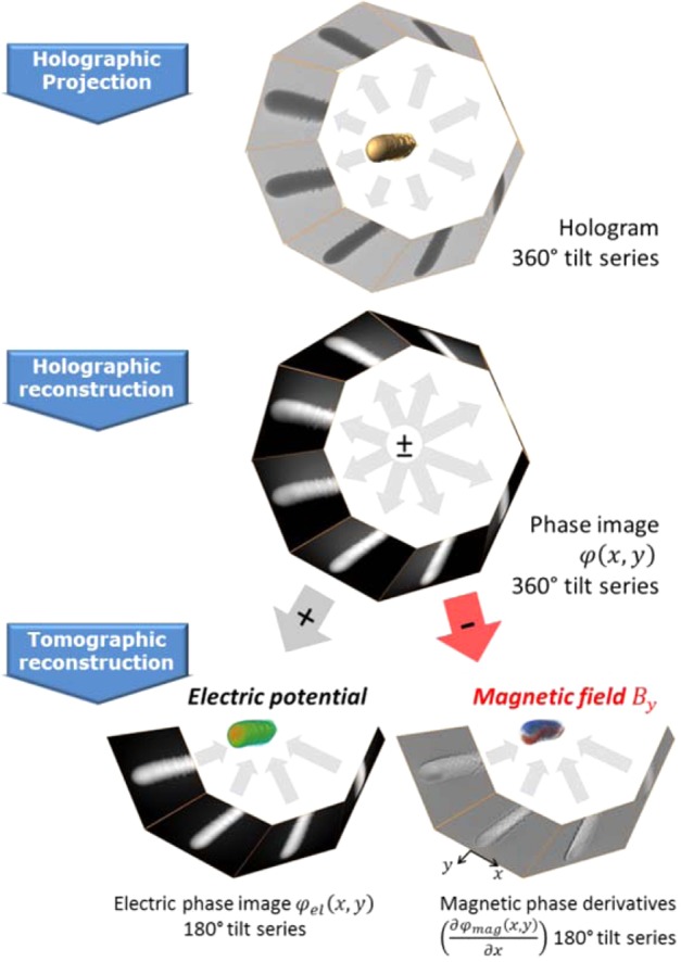
Principle of electron holographic tomography for the 3D reconstruction of internal electro-magnetic fields in nanostructures. A tilt series of holograms covering a tilt range of 360° is recorded. From the holograms, the phase image tilt series is reconstructed and separated in its electric/magnetic part by calculating half of the sum/difference between opposite (180° tilted) projections. To obtain the 3D electric potential the tilt series of electric phase images is used for tomographic reconstruction. To obtain the 3D axial magnetic field component the magnetic phase images need to be differentiated in direction perpendicular to the tilt axis prior the tomographic reconstruction.
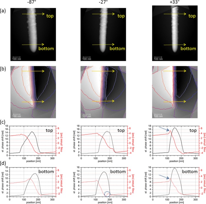
Representative phase images of the tilt series are presented in Figure 2. Both, electric and magnetic contributions are displayed as gray values (Figure 2a), and the magnetic part is visualized additionally as phase isolines (Figure 2b). As illustrated by line profiles (Figure 2c,d), the electric phase shift (black) is proportional to the projected mean inner potential (MIP),28,29 whereas the magnetic phase shift (red) shows a negative slope due to the magnetic flux within the NW and a positive slope due to the returning magnetic flux in vacuum (stray field). In vacuum, also the electric phase shift exhibits a gradient implying an electrical fringing field which is caused by charging of the NW, in particular its oxide surface by the electron beam. However, the constant phase gradient within the whole tilt series indicates that the charging was constant at the entire duration of the experiment. Therefore, artifacts in magnetic phase shift due to varying electrical fringing fields can be excluded. Most interestingly, in the magnetic phase images, there is a region at the apex of the NW (marked with a dashed circle in the profile Figure 2d at −27° tilt angle), where the slope direction changes within the sample. This slope inversion is also visible in other projections, which suggests a change in the magnetization direction at the apex of the NW. However, the profiles also exhibit artifacts at the edges of the sample, e.g. at positions marked with dashed arrows in the profiles Figure 2c,d at +33° tilt angle. These may be attributed to misalignment errors, lens aberrations, and slight contaminations at the surface, introducing phase variations of neither magnetic nor electrostatic origin. Consequently, the reconstructed 3D distribution of the magnetic field cannot be interpreted in these regions as discussed further below.
Figure 2.
(a)/(b) Electric/magnetic phase images taken at −87°, −27°, and +33° tilt angle. (c)/(d) Line profiles along the arrows marked in (a) and (b) representing the electric (black) and magnetic (red) phase shift. The circle in (d) at −27° indicates the change of the phase gradient due to the change of magnetization direction in a small domain at the tip. The arrows in (c,d) at +33° indicate artifacts in the magnetic phase shift at the edge of the sample.
Following eq 2, the projections of the axial component By are now obtained by a directional numerical differentiation of the magnetic phase images perpendicular to the tilt axis. In our experiment, tilt axis and longitudinal axis of the NW are almost parallel, comprising only a small angle of 3°. Therefore, longitudinal B component and its projection onto the tilt axis differ only slightly by ca. 0.1% and can be considered identical when discussing the results of the ensuing tomographic reconstruction. The latter was carried out using the weighted simultaneous iterative reconstruction technique (W-SIRT)30 with 5 iterations. The W-SIRT developed in-house uses at each SIRT iteration a weighted back-projection instead of a simple back-projection used in conventional SIRT.
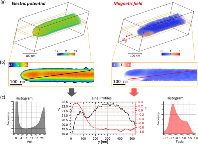
This leads to improved convergence properties of the tomographic reconstruction. Here, the number of iterations was determined by visually inspecting the spatial resolution and noise of the reconstruction for an optimal balance. The spatial resolution of the 3D reconstruction is below 10 nm, as we demonstrate by determination of the width of the edge-spread function in six different directions on a representative cross-section of the Co NW (see the Supporting Information). The 3D distributions of the electric potential and the axial magnetic induction of the Co NW reconstructed by EHT are shown in Figure 3. Here, we analyze only the B-field inside the sample where the corresponding electric potential is V ≥ 16 V, because the edge regions are affected by artifacts as mentioned above. A tomographic reconstruction of the stray field only is shown in the Supporting Information.
Figure 3.
Electric potential and axial magnetic B-field component of a Co nanowire. (a) Volume rendering, i.e. the colors correspond to the potential/B-field values. (b) 15 nm thick 2D slices through the 3D data as indicated by the orange boxes in (a). (c) Histograms of 3D volumes and 1D line profiles along the arrows marked in (b). The peak in the histogram of the electric potential at 21.5 V can be interpreted as the mean inner potential of this Co NW. The most frequent value in the histogram of the magnetic induction is at −0.9 T.
Selected cross sections (Figure 3b) at positions indicated by orange boxes in the volume visualization (Figure 3a) reveal that the intrinsic electric potential is virtually homogeneous along the axial direction suggesting a homogeneous chemical composition. In contrast to that, the magnetic field exhibits a domain structure consisting of one large domain (blue, By = −0.9 T) and a small domain (red, By = −0.3 T) at the apex with the magnetization pointing in opposite direction.
These findings are supported by the histograms of 3D volumes and 1D line profiles (Figure 3c) along the arrows marked in Figure 3b. The most frequent electric potential value in the histogram is found at 21.5 V, which is lower than the theoretical MIP value of pure Co (29.5 V)31 calculated using neutral atom potentials of Rez et al.32
The observed difference is mainly caused by both the mass density and the Co purity of the nanocrystalline wire produced by FEBID being lower compared to bulk material, hence reducing the mean inner potential. The Co purity was determined by STEM-EDX (see the Supporting Information for details) and a grain size of 3–6 nm in diameter was revealed by TEM analysis.33 Furthermore, the theoretical crystal potential may be overestimated when using independent neutral atom potentials without taking into account chemical bonding.
Similarly, the average magnetic induction along the wire axis of 0.9 T is lower than the value expected for pure bulk cobalt (1.76 T).31 This reduction of magnetization has been observed in electron holography experiments for similar Fe nanowires grown by FEBID33 and is mainly caused by low purity of the material forming the NW, as well as demagnetization fields associated with the specimen geometry reducing the magnetization inside the sample. Another possible source of error may be the fact that we determine the average magnetic induction only from the axial B-field component instead of from the magnitude of the entire vector field |B|. However, the simulation results discussed below suggest that the contributions of the other two B-field components to the histogram are indeed small (Figure 5e), i.e. the peak positions of the By and -|B| histogram differ only by 10 mT. Furthermore, the electric potential decreases from the center (red) to the surface (green) in radial direction, whereas the magnetic induction remains constant. The reduced potential can be explained by oxidation of the surface as confirmed by STEM-EDX (see the Supporting Information) and the reduced mass density as confirmed by tomographic reconstruction of mass thickness (see the Supporting Information). According to the line profile in Figure 3c, there is a drop in the electric potential at the position where the magnetic induction changes its direction. A lower electric potential may indicate a structural modulation of material resulting in a local reduction of the magnetization at that area. This would favor the formation of the observed magnetic domain. A more detailed explanation of such an electromagnetic coupling is however beyond the scope of this article, and we restrict ourselves to verify our results by micromagnetic simulations in the following.
Figure 5.
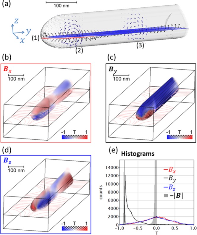
Induction map B of the Co NW obtained from micromagnetic simulation. (a) Iso-surface with longitudinal slice (1) representing By and cross sections (2) and (3) visualized by arrow plots. In slice (1), the out-of-plane components are displayed as vectors. In the cross sections (2) and (3), the twist of magnetic induction is illustrated by the opposite azimuthal direction of the vectors. (b-d) Volume rendering of the three B-field components with field lines in the x-y plane. (e) Histograms of B-field components and negative of the total magnitude.
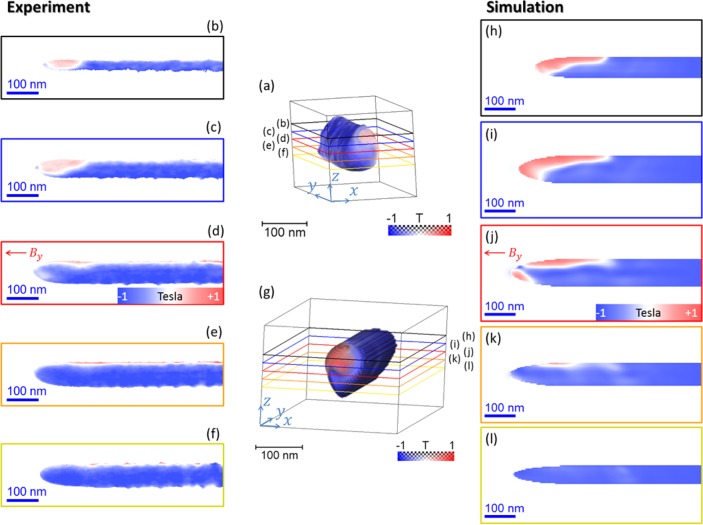
Given the reconstructed 3D distribution of the axial component of the magnetic induction we may now elucidate the 3D distribution of all three components and the origin of the inverse apex domain with the help of micromagnetic simulations (see the methods section for details). In Figure 4 representative slices through the Co NW and corresponding simulation are displayed. Most of the spins are aligned along the y-direction, forming a monodomain state (blue region in Figure 4) along the wire axis, as observed experimentally. Furthermore, a closure domain is present at the tip of the wire representing a C state with a 180° domain wall which is in excellent agreement with the experimental result. This remanent magnetization state is common to soft magnetic nanostructures,34 where the strong demagnetizing field twists the magnetization at their end to avoid the generation of magnetic charges at the surface. The simulations shown here were performed with a saturation magnetization corresponding to the experimentally obtained magnetic induction. For this value, an exchange constant smaller than the one normally used for Co bulk was needed in order to get a closure domain at remanence for the given dimensions, whereas simulations using higher exchange values resulted in single monodomain states (see methods). The low exchange value needed to reproduce the experimental results may be due to the low purity of cobalt grown by FEBID, but it could also be caused by effects not considered in the simulations, such as roughness, presence of defects, local change of composition along the wire, or influence of local magnetocrystalline anisotropy.35,36 These can also explain small differences in the structure of the domain between simulation and experiments: For example, in the simulation the inversion domain is formed in the thicker region, whereas in the experiment it is formed in the thinner region of the “egg-shaped” cross-section and is more extended along the edge (Figure 4 d,e and j,k). In cylindrical nanowires as the one studied here, curling of the magnetization along the surface is expected in order to minimize the dipolar energy.37 This is confirmed by the micromagnetic simulation, as observed in Figure 5, where the three B-field components are shown. In particular, Figure 5a depicts how the azimuthal direction of the NW is inverted toward the apex of the NW. However, the separate visualization of the three B-field components in Figure 5b-d and the histogram (Figure 5e) show that the overall curling effect is small, with the component along the wire axis By mostly dominant compared with the other two.
Figure 4.
Comparison between experimentally reconstructed (a-f) and simulated (g-l) B-field in axial (y-) direction. In the volume rendering of experimental (a) and simulated (g) magnetic induction maps, the z-positions of the slices are indicated as (b-f) and (h-l), respectively.
Conclusion
In summary, we have demonstrated that electron holographic tomography can be used to quantitatively reconstruct the 3D magnetic field configuration within ferromagnetic nanostructures. As an example, we observed in the reconstructed axial B-field component of a Co NW a small closure domain at the tip with a spatial resolution below 10 nm and a signal resolution of 0.1 T. In a next step EHT has to be extended to reconstruct all components of the magnetic field at the above-noted figure of merits. We envisage the technique to open new pathways to the characterization of nanoscale ferromagnetic elements, such as spin valves, read-write magnetic heads, magnetic sensors, and magnetic logic devices.
Experimental Section
Growth of a Cobalt Nanowire by FEBID
The growth was performed in an FEI Helios 600 dual beam system equipped with a 30 kV FEG and a Ga+ liquid metal source in the same chamber. In this work, the substrate was a Cu rod of 1 mm in diameter ending in a nanotip, on which the cobalt pillar was grown. The end of the tip was cut and sharpened using focused ion milling (Figure S1) to ensure that the pillar rested on the salient point of the substrate. The parameters used during the growth and more information on the growth process can be found in the Supporting Information and in refs (38 and 39).
Holographic Tilt Series Acquisition
The Cu rod with the Co NW was transferred to a dedicated electron tomography holder (model 2050, Fischione Instruments), and plasma was cleaned to remove contamination of the NW surface. A tilt series consisting of object and object-free (empty) holograms was recorded using the Qu-Ant-EM, a FEI Titan3 TEM operated at 300 kV in non Cs-corrected Lorentz mode (objective lens off). A Möllenstedt biprism operating at 200 V was introduced in the SA aperture plane to create the holograms. In order to increase the width of the interference area, the diffraction lens current was increased to its maximum strength. The tilt series was acquired within the angular range from 0° to 360° in 3° steps. The electron holograms were acquired with a US1000XP Gatan CCD camera (binning 1, 5 s exposure time), at a pixel size of 0.37 nm and a fringe spacing of 2.2 nm.
Holographic and Tomographic Reconstruction
All image processing steps were performed in Gatan Inc.’s Digital Micrograph. The resolution of the reconstructed object exit wave is 4.6 nm, determined by the size of the numerical mask used in the Fourier reconstruction. The tilt series of phase images was divided into two parts, one below and one above 180° tilt angle. Then, both tilt series were prealigned separately by cross-correlation to correct for coarse displacements between successive projections. Furthermore, the second tilt series was flipped perpendicular to the tilt axis to convert the 180° rotation between corresponding phase images into a mirroring with respect to the image plane. Then, each pair of phase images was aligned to each other by applying a linear affine transformation on the “flipped” phase images, which considered displacements, rotation, and direction-dependent magnification changes. To perform the exact fine alignment, i.e., the accurate determination of the tilt axis and correction for subpixel displacement, we have used a self-implemented center-of-mass method for correction of displacements perpendicular to the tilt axis in the sinograms and the common line approach for the displacement correction parallel to the tilt axis. The magnetic phase tilt series was aligned using parameters as determined from the electric phase tilt series, which has a higher signal-to-noise ratio than the magnetic one and therefore yields more accurate parameters. Before computation of the derivatives the magnetic phase images were smoothed slightly by a Median filter with a 3 × 3 Pixel kernel.
Micromagnetic Simulations
A static micromagnetic simulation of the remanent state of the Co FEBID NW was performed by the GPMagnet software package,40 which solves the Landau-Lifschitz-Gilbert equation. The computation ran parallelized on an efficient graphics processing unit (GPU). The 3D shape of the NW was adapted from the experimental tomogram and constructed with a maximum length of 1000 nm by assembling cubic cells of 3.5 × 3.5 × 3.5 nm3. The “egg-shaped” cross-section of the NW model was varied from 90 to 110 nm, and the tip is spherical. The micromagnetic calculations were performed for the NW placed inside a volume of 301.0 × 1200.5 × 220.5 nm3. Thus, the aspect ratio (length/diameter ≈1000/100 = 10) is large enough to align the magnetization along the nanowire at remanence via shape anisotropy. The magnetic parameters for the Co NW have been chosen from the experimental data: The saturation magnetization (Ms) was set to 0.72 × 10⁶ A/m, as estimated from the measured value of the B-field; the exchange constant A was suitably tuned until a small magnetic domain with a similar size of that experimental one was formed at the tip. We achieved such a condition using A ≤ 0.4 × 10⁻¹¹ J/m, smaller than the value for pure Co (1–3 × 10–11 J/m). If we use A ≥ 0.4 × 10⁻¹¹ J/m, the closure domain is not formed for the given Ms. The magnetocrystalline anisotropy was neglected due to the nanocrystalline morphology of the NW, composed of small grains of about 5 nm size randomly oriented. For this static simulation, an initial magnetization configuration was considered, with all spins oriented along the y-direction. The simulation was iterated using a second order predictor corrector until minimizing the total energy of the system.
Acknowledgments
This work was supported by the European Union under the Seventh Framework Program under a contract for an Integrated Infrastructure Initiative Reference 312483-ESTEEM2. S.B. and A.B. gratefully acknowledge funding by ERC Starting grants number 335078 COLOURATOMS and number 278510 VORTEX. A.F.-P. acknowledges an EPSRC Early Career fellowship and support from the Winton Foundation. E.S., C.G., and L.A.R. acknowledge the French ANR program for support though the project EMMA. J.M.D.T. and C. M. acknowledge the Spanish MINECO projects MAT2014-51982-C2-1-R and MAT2014-51982-C2-2-R, respectively.
Supporting Information Available
The Supporting Information is available free of charge on the ACS Publications website at DOI: 10.1021/acs.chemmater.5b02723.
Growth of cobalt nanowire by FEBID, STEM-EDX analysis, medium scale HAADF-STEM tomography, perturbation of reference wave during holographic acquisition, stray field reconstruction of the nanowire, comparison between 3D reconstructions of potential and elastic attenuation (PDF)
Movie of phase tilt series (MPG)
Movie of 3D electric potential (MPG)
Movie of 3D magnetic induction map (MPG)
In compliance with EPSRC's open access inititive, the data in this paper is available from https://www.repository.cam.ac.uk/handle/1810/250343.
Author Contributions
D.W., A.B., E.J., and L.A.R. performed the EHT experiment. D.W. aligned, reconstructed, and evaluated the 3D data. L.S. prepared the sample. A.F.-P. and J.M.D.T. contributed to the preparation of the sample. L.A.R. performed the micromagnetic simulation. A.L. performed the magnetic stray field reconstruction. D.W. wrote the manuscript. A.F.-P., A.B., E.S., A.L., L.A.R., L.S., and S.B. contributed to manuscript writing. E.S, S.B., and H.L. initiated the EHT study. All the authors discussed the results and commented on the manuscript.
The authors declare no competing financial interest.
Supplementary Material
References
- Parkin S. S. P.; Hayashi M.; Thomas L. Magnetic Domain-Wall Racetrack Memory. Science 2008, 320, 190–194. 10.1126/science.1145799. [DOI] [PubMed] [Google Scholar]
- Lavrijsen R.; Lee J.-H.; Fernandez-Pacheco A.; Petit D. C. M. C.; Mansell R.; Cowburn R. P. Magnetic ratchet for three-dimensional spintronic memory and logic. Nature 2013, 493, 647–650. 10.1038/nature11733. [DOI] [PubMed] [Google Scholar]
- Nasirpouri F.; Nogaret A.. Nanomagnetism and Spintronics - Fabrication, Materials, Characterization and Applications; World Scientific: 2011. [Google Scholar]
- Shinjo T.Nanomagnetism and Spintronics; Elsevier Science: 2013. [Google Scholar]
- Stamps R. L.; Breitkreutz S.; Akerman J.; et al. The 2014 Magnetism Roadmap. J. Phys. D: Appl. Phys. 2014, 47, 333001. 10.1088/0022-3727/47/33/333001. [DOI] [Google Scholar]
- Zhu Y.Modern Techniques for Characterizing Magnetic Materials; Springer: 2005. [Google Scholar]
- Hopster H.; Oepen H. P.. Magnetic Microscopy of Nanostructures; Springer: 2006. [Google Scholar]
- Aharonov Y.; Bohm D. Significance of Electromagnetic Potentials in the Quantum Theory. Phys. Rev. 1959, 115, 485–491. 10.1103/PhysRev.115.485. [DOI] [Google Scholar]
- Tonomura A. Applications of electron holography. Rev. Mod. Phys. 1987, 59, 639–669. 10.1103/RevModPhys.59.639. [DOI] [Google Scholar]
- Lichte H.; Lehmann M. Electron holography - basics and applications. Rep. Prog. Phys. 2008, 71, 016102. 10.1088/0034-4885/71/1/016102. [DOI] [Google Scholar]
- Dunin-Borkowski R. E.; McCartney M. R.; Frankel R. B.; Bazylinski D. A.; Pósfai M.; Buseck P. R. Magnetic Microstructure of Magnetotactic Bacteria by Electron Holography. Science 1998, 282, 1868–1870. 10.1126/science.282.5395.1868. [DOI] [PubMed] [Google Scholar]
- Snoeck E.; Gatel C.; Lacroix L. M.; et al. Magnetic Configurations of 30 nm Iron Nanocubes Studied by Electron Holography. Nano Lett. 2008, 8, 4293–4298. 10.1021/nl801998x. [DOI] [PubMed] [Google Scholar]
- Biziere N.; Gatel C.; Lassalle-Balier R.; Clochard M. C.; Wegrowe J. E.; Snoeck E. Imaging the Fine Structure of a Magnetic Domain Wall in a Ni Nanocylinder. Nano Lett. 2013, 13, 2053–2057. 10.1021/nl400317j. [DOI] [PMC free article] [PubMed] [Google Scholar]
- Javon E.; Gatel C.; Masseboeuf A.; Snoeck E. Electron holography study of the local magnetic switching process in magnetic tunnel junctions. J. Appl. Phys. 2010, 107, 09D310. 10.1063/1.3358219. [DOI] [Google Scholar]
- Beleggia M.; Kasama T.; Dunin-Borkowski R. E. The quantitative measurement of magnetic moments from phase images of nanoparticles and nanostructures--I. Fundamentals. Ultramicroscopy 2010, 110, 425–432. 10.1016/j.ultramic.2009.10.007. [DOI] [Google Scholar]
- Lai G.; Hirayama T.; Ishizuka K.; Tonomura A. Three-dimensional reconstruction of electric-potential distribution in electron-holographic interferometry. Appl. Opt. 1994, 33, 829–833. 10.1364/AO.33.000829. [DOI] [PubMed] [Google Scholar]
- Midgley P. A.; Dunin-Borkowski R. E. Electron tomography and holography in materials science. Nat. Mater. 2009, 8, 271–280. 10.1038/nmat2406. [DOI] [PubMed] [Google Scholar]
- Wolf D.; Lubk A.; Röder F.; Lichte H. Electron holographic tomography. Curr. Opin. Solid State Mater. Sci. 2013, 17, 126–134. 10.1016/j.cossms.2013.05.002. [DOI] [Google Scholar]
- Lai G.; Hirayama T.; Fukuhara A.; Ishizuka K.; Tanji T.; Tonomura A. Three-dimensional reconstruction of of magnetic vector fields using electron-holographic interferometry. J. Appl. Phys. 1994, 75, 4593–4598. 10.1063/1.355955. [DOI] [PubMed] [Google Scholar]
- Phatak C.; Petford-Long A. K.; De Graef M. Three-Dimensional Study of the Vector Potential of Magnetic Structures. Phys. Rev. Lett. 2010, 104, 253901. 10.1103/PhysRevLett.104.253901. [DOI] [PubMed] [Google Scholar]
- Phatak C.; Beleggia M.; De Graef M. Vector field electron tomography of magnetic materials: Theoretical development. Ultramicroscopy 2008, 108, 503–513. 10.1016/j.ultramic.2007.08.002. [DOI] [PubMed] [Google Scholar]
- Lubk A.; Wolf D.; Simon P.; Wang C.; Sturm S.; Felser C. Nanoscale three-dimensional reconstruction of electric and magnetic stray fields around nanowires. Appl. Phys. Lett. 2014, 105, 173110. 10.1063/1.4900826. [DOI] [Google Scholar]
- Tanigaki T.; Takahashi Y.; Shimakura T.; Akashi T.; Tsuneta R.; Sugawara A.; Shindo D. Three-Dimensional Observation of Magnetic Vortex Cores in Stacked Ferromagnetic Discs. Nano Lett. 2015, 15, 1309–1314. 10.1021/nl504473a. [DOI] [PubMed] [Google Scholar]
- Kremer J. R.; Mastronarde D. N.; McIntosh J. R. Computer Visualization of Three-Dimensional Image Data Using IMOD. J. Struct. Biol. 1996, 116, 71–76. 10.1006/jsbi.1996.0013. [DOI] [PubMed] [Google Scholar]
- Tonomura A.; Matsuda T.; Endo J.; Arii T.; Mihama K. Holographic interference electron microscopy for determining specimen magnetic structure and thickness distribution. Phys. Rev. B: Condens. Matter Mater. Phys. 1986, 34, 3397–3402. 10.1103/PhysRevB.34.3397. [DOI] [PubMed] [Google Scholar]
- Wolf D.; Lubk A.; Lichte H.; Friedrich H. Towards automated electron holographic tomography for 3D mapping of electrostatic potentials. Ultramicroscopy 2010, 110, 390–399. 10.1016/j.ultramic.2009.12.015. [DOI] [PubMed] [Google Scholar]
- Lehmann M.; Lichte H. Tutorial on Off-Axis Electron Holography. Microsc. Microanal. 2002, 8, 447–466. 10.1017/S1431927602020147. [DOI] [PubMed] [Google Scholar]
- Bethe H. Theory on the diffraction of electrons in crystals. Ann. Phys. 1928, 87, 55–129. 10.1002/andp.19283921704. [DOI] [Google Scholar]
- O’Keeffe M.; Spence J. C. H. On the average Coulomb potential and constraints on the electron density in crystals. Acta Crystallogr., Sect. A: Found. Crystallogr. 1994, 50, 33–45. 10.1107/S010876739300474X. [DOI] [Google Scholar]
- Wolf D.; Lubk A.; Lichte H. Weighted simultaneous iterative reconstruction technique for single-axis tomography. Ultramicroscopy 2014, 136, 15–25. 10.1016/j.ultramic.2013.07.016. [DOI] [PubMed] [Google Scholar]
- Dunin-Borkowski R. E.; McCartney M. R.; Smith D. J.; Parkin S. S. P. Towards quantitative electron holography of magnetic thin films using in situ magnetization reversal. Ultramicroscopy 1998, 74, 61–73. 10.1016/S0304-3991(98)00023-0. [DOI] [Google Scholar]
- Rez D.; Rez P.; Grant I. Dirac-Fock calculations of X-ray scattering factors and contributions to the mean inner potential for electron scattering. Acta Crystallogr., Sect. A: Found. Crystallogr. 1994, 50, 481–497. 10.1107/S0108767393013200. [DOI] [Google Scholar]
- Takeguchi M.; Shimojo M.; Furuya K. Fabrication of magnetic nanostructures using electron beam induced chemical vapour deposition. Nanotechnology 2005, 16, 1321–1325. 10.1088/0957-4484/16/8/057. [DOI] [Google Scholar]
- Usov N. A.; Zhukov A.; Gonzalez J. Remanent Magnetization States in Soft Magnetic Nanowires. IEEE Trans. Magn. 2006, 42, 3063–3065. 10.1109/TMAG.2006.880104. [DOI] [Google Scholar]
- New R. M. H.; Pease R. F. W.; White R. L. Effect of magnetocrystalline anisotropy in single-domain polycrystalline cobalt islands. IEEE Trans. Magn. 1995, 31, 3805–3807. 10.1109/20.489778. [DOI] [Google Scholar]
- Hausmanns B.; Krome T. P.; Dumpich G. Magnetoresistance and magnetization reversal process of Co nanowires covered with Pt. J. Appl. Phys. 2003, 93, 8095–8097. 10.1063/1.1540054. [DOI] [Google Scholar]
- Jamet S.; Rougemaille N.; Toussaint J.-C.; Fruchart O. Head-to-head domain walls in one-dimensional nanostructures: an extended phase diagram ranging from strips to cylindrical wires. arXiv.org, e-Print Arch., Condens. Matter 2014, 1412, 0679. [Google Scholar]
- Fernandez-Pacheco A.; Serrano-Ramon L.; Michalik J. M.; et al. Three dimensional magnetic nanowires grown by focused electron-beam induced deposition. Sci. Rep. 2013, 3, 1492. 10.1038/srep01492. [DOI] [PMC free article] [PubMed] [Google Scholar]
- Serrano-Ramón L.; Córdoba R.; Rodrigues L. A.; et al. Ultrasmall Functional Ferromagnetic Nanostructures Grown by Focused Electron-Beam-Induced Deposition. ACS Nano 2011, 5, 7781–7787. 10.1021/nn201517r. [DOI] [PubMed] [Google Scholar]
- Lopez-Diaz L.; Aurelio D.; Torres L.; et al. Micromagnetic simulations using Graphics Processing Units. J. Phys. D: Appl. Phys. 2012, 45, 323001. 10.1088/0022-3727/45/32/323001. [DOI] [Google Scholar]
Associated Data
This section collects any data citations, data availability statements, or supplementary materials included in this article.


