

Abstract
The performance of an 8 × 8 array of 6.0 × 6.0 mm2 (active area) SiPMs was evaluated for PET applications using crystal arrays with different pitch sizes (3.4 mm, 1.5 mm, 1.35 mm and 1.2 mm) and custom designed five-channel front-end readout electronics (four channels for position information and one channel for timing information). The total area of this SiPM array is 57.4 × 57.4 mm2, and the pitch size is 7.2 mm. It was fabricated using enhanced blue sensitivity SiPMs (MicroFB-60035-SMT) with peak spectral sensitivity at 420 nm. The performance of the SiPM array was characterized by measuring flood histogram decoding quality, energy resolution, timing resolution and saturation at several bias voltages (from 25.0 V to 30.0 V in 0.5 V intervals) and two different temperatures (5 °C and 20 °C). Results show that the best flood histogram was obtained at a bias voltage of 28.0 V and 5 °C and an array of polished LSO crystals with a pitch as small as 1.2 mm can be resolved. No saturation was observed up to a bias voltage of 29.5 V during the experiments, due to adequate light sharing between SiPMs. Energy resolution and timing resolution at 5 °C ranged from 12.7 ± 0.8% to 14.6 ± 1.4 % and 1.58 ± 0.13 ns to 2.50 ± 0.44 ns, for crystal array pitch sizes of 3.4 mm and 1.2 mm respectively. Superior flood histogram quality, energy resolution and timing resolution were obtained with larger crystal array pitch sizes and at lower temperature. Based on our findings, we conclude that this large-area SiPM array can serve as a suitable photodetector for high-resolution small-animal PET or dedicated human brain PET scanners.
Keywords: Nuclear medicine, Instrumentation, PET, Silicon photomultiplier
I. Introduction
SILICON photomultipliers (SiPMs) are considered the photodetector of choice for fully integrated PET/MRI systems due to their insensitivity to magnetic fields and compact size [1-3]. Previous studies have shown that the performance of SiPM-based PET detectors and systems built with SiPMs are unperturbed in the presence of a strong magnetic field (e.g. [4-6]). During the last ten years, a variety of SiPM-based PET detector modules or prototype PET scanners for small-animal and human imaging have been developed (e.g. [5], [7-11]). However, most of these detector modules were based on SiPM arrays with a total area of less than 20 × 20 mm2, a limitation imposed by the higher noise of early-generation SiPMs, and the complexity to design high-performance readout electronics without compromising the detector performance. One-to-one coupling of crystals to SiPMs with individual electronic channels for each SiPM, is a straightforward method and excellent single detector performance (energy resolution and timing resolution) is maintained [12-14]. However, one-to-one coupling and individual detector readout requires multi-channel readout and the detector’s intrinsic spatial resolution is limited by the size of the individual SiPM. To overcome these constraints, light-sharing and signal multiplexing is normally used. Although the number of readout channels is decreased, signal multiplexing combines the noise of all SiPMs, thus decreasing the performance of detector modules [15-16]. To provide an acceptable trade-off between performance and number of read-out channels, 4 × 4 arrays of SiPMs have been the focus of attempts to resolve crystal arrays with a fine pitch size. Due to edge effects in the light sharing distribution, in order to resolve all the crystals in the crystal array, the crystal blocks are typically recessed from the edge of the device by ~2-3 mm. This results in a packing fraction of just 50% - 60% when 4 × 4 SiPM arrays are used to resolve crystal arrays with a pitch size of ~ 1 mm [7], [11], [17-18].
One way to improve the effective usable area of a SiPM array is to use large-area SiPM arrays or position sensitive SiPMs (PS-SiPMs) [19-23]. Crystal arrays with pitch sizes of 0.45 mm have been clearly resolved using PS-SiPMs and the effective area of the photodetector can be > 90% [20-21]. However, the performance of PS-SiPMs reduces significantly with increasing area making it difficult to develop SiPM-based PET detectors with areas > 20 × 20 mm2 at present [20].
Large-area PMTs, such as the Hamamatsu PMT H8500 and H9500, have been successfully used for high resolution PET scanners [24-27], however, PMTs are sensitive to magnetic fields, and special effort/techniques (for example optical fiber coupling are required to extract the scintillation photons out of the MRI bore before detection by the photodetector for PET/MRI applications. This leads to signal losses and a reduction in signal-to-noise ratio [28-29].
In recent developments, the noise of SiPMs has been significantly reduced, and photon detector efficiency (PDE) has been improved using new manufacturing technologies [30-31], making it possible to use signal multiplexing to read out signals from large area SiPM arrays. Large-area SiPM arrays (> 50 × 50 mm2), consisting of hundreds of ~ 3 × 3 mm2 SiPM pixels, have been investigated by others. The results show that crystal arrays with ~1 mm crystal pitch can be resolved, and the effective area is greater than 90% of the physical device size [16], [32].
An 8 × 8 array of 6 × 6 mm2 SiPMs was fabricated based on the MicroFB-60035-SMT SiPM by SensL (SensL Technologies Ltd., Ireland). The package size of each SiPM is 7 × 7 mm2. The MicroFB series is designed for high volume applications and has been extensively characterized and assessed for reliability [33]. The number of SiPMs is less than half that used in a SiPM array consisting of 3 × 3 mm2 SiPMs with similar area, simplifying the design and implementation of the readout electronics [16], [34]. In this paper, the performance of this new SiPM array was evaluated using scintillator arrays of varying pitch sizes (from 1.2 mm to 3.4 mm) and light sharing using different light guides. Performance was evaluated by measuring flood histogram quality, energy resolution, timing resolution, and saturation over a range of SiPM bias voltages and at two different temperatures (5 °C and 20 °C).
II. Materials and Methods
A. SiPM array and Crystal array
The total area of the 8 × 8 MicroFB SiPM array is 57.4 × 57.4 mm2, and each SiPM pixel has an active size of 6 × 6 mm2, containing 18980 35 μm (active area) microcells with a fill factor of 64%. The center-to-center distance of two adjacent SiPM pixels is 7.2 mm (Fig.1 (b)), leaving a 1.2 mm dead space between the active area of adjacent SiPM pixels. The MicroFB devices are fabricated using a p-on-n structure that significantly improves photon detection efficiency (PDE) for blue light [33]. The breakdown voltage of the MicroFB SiPMs were all within ± 0.25 V of 24.7 V, with a standard deviation of 73 mV [33]. Operating at an over-voltage of 2.5V, these devices exhibit 31% PDE for light with wavelength 420 nm, well-matched to the emission spectra of LSO or LYSO, which are widely used as crystals in PET detectors [35-36].
Fig. 1.
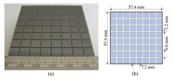
(a) Photograph and (b) schematic of SiPM array.
The four crystal arrays used in the experimental tests are listed in Table I. Enhanced specular reflector (ESR, 3M) was used in all crystal arrays to optically isolate the crystals. The 15 × 15 LYSO array was used to optimize bias voltage and the other three crystal arrays were used to study the crystal identification ability of the SiPM array. To ensure light sharing between SiPMs, clear acrylic slabs were used as light guides and coupled between the scintillator arrays and SiPM surface using optical grease (BC-630, Saint Gobain). The light guide thickness (1.0 to 3.4 mm) was optimized to produce the best flood histogram for each array and these values are also given in Table I. The 15 × 15 LYSO array was also directly coupled to the SiPM array in some experiments. For each of the arrays tested, the signals from all 64 SiPMs were used to construct the flood histogram, even though the crystal array only covers a small subset of the SiPMs in the array. A 3.7 MBq 68Ge point source, located 100 mm above the front face of the scintillator arrays, was used to irradiate the crystals with 511 keV photons.
TABLE I.
Scintillator Arrays
| Scintillator | Array size | Crystal size / mm3 |
Pitch Size / mm |
Light guide /mm |
|---|---|---|---|---|
| LYSO | 15 × 15 | 3.34 × 3.34 × 20 | 3.4 | 1.2 |
| LYSO | 9 × 9 | 1.43 × 1.43 × 12 | 1.5 | 2.8 |
| LYSO | 8 × 8 | 1.28 × 1.28 × 12 | 1.35 | 3.0 |
| LSO | 10 × 10 | 1.13 × 1.13 × 14 | 1.2 | 3.2 |
To position the crystal array, light guide and SiPM array consistently for different measurements, holders were fabricated using 3D printing methods. The detector module was placed in a light-tight dark-box and cooled with dry air from an airjet sample cooler (XR 401, FTS Systems, Inc.). The detector temperature was monitored using a Type K thermocouple (TSTEMP10K, Eutech Inst.). The thermocouple sensor was attached to the back side of the SiPM array. To reduce moisture inside the experimental box, dry room temperature air was sent to the box for 30 mins before any experiments. During experiments, the temperature of the dry air was changed at a rate of approximately 0.3 °C/min to reach the desired temperature.
B. Front-end detector Readout
Each MicroFB SiPM pixel has two outputs, a fast output and a standard anode-cathode output, which were used for timing and energy information respectively [33]. The fast output is the derivative of the internal fast switching of the microcell in response to the detection of a single photon. The gains of the standard output and the fast output are 3 × 10⁶ and 4.3 × 10⁴ respectively at an overvoltage of 2.5V. The fast output provides low output capacitance (48 pf for the device used in this SiPM array) and is designed with minimal parasitic resistance [33]. Fast output signals have a rise time of ~1 ns but the gain is only 2%-4% of the standard output. Good timing resolution can be obtained using the fast output [37-38]. In our custom front-end electronics (Fig. 2), the standard outputs of each SiPM were individually amplified and summed by rows and columns, generating 8 row-sum signals and 8 column-sum signals. The row/column signals were weighted by applying a weighted gain to each row and column proportional to its location along each axis, generating four signals (X+, X− and Y+, Y−) for position information [39-40]. All the analog operations were implemented using AD8056 amplifiers (Analog Device, Inc.). The four position signals were further amplified and shaped by a spectroscopy amplifier (N586B, CAEN) and digitized with a PowerDAQ (PD2MFS, United Electronic Industries) board [41]. The centroid of the scintillation light position (x, y) and the deposited energy E from the 511 keV photon interaction were calculated as follows:
| (1) |
| (2) |
Fig. 2.
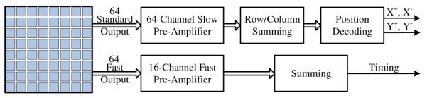
Schematic showing front-end readout.
The fast outputs of each group of 2 × 2 SiPMs were connected together through 50 Ohm resistors (each fast output has its own 50 Ohm resistor) and amplified using THS3202 amplifiers (Texas Instruments Inc.). All 16 amplified fast signals were summed together to form one global timing signal and a constant fraction discriminator (CFD) (584, ORTEC) was used to generate a time-stamp and to trigger the DAQ board.
To simplify the electronics design, a common bias voltage was applied to all 64 SiPMs in the array. The bias voltage was generated by a DC power module (N6736B and N6700B, Agilent Technologies, Inc.), and a bias voltage filter was designed and implemented on the front-end readout board.
C. Noise
Dark noise is one of the key characteristics of SiPMs. It is caused by thermally-generated charge carriers reaching the avalanche region. The dark noise rate increases with higher bias voltage and temperature [1]. The noise is consistent in time at a specific working condition (bias voltage and temperature) and uncorrelated to the pulses resulting from photon absorption. The typical dark count rate of these SiPMs is 33.3 kHz/mm2 at an overvoltage of 2.5 V and a temperature of 21 °C. The noise of the SiPM array was quantified by measuring the FHWM of a Gaussian fit to the noise distribution on the signal base line. The signal was the sum of the four position signals (X+, X− and Y+, Y−), acquired by triggering the PowerDAQ using the internal trigger generated by the computer clock [21],[41]. The dark noise was measured with and without the 15 × 15 crystal array present.
D. Flood histogram quality
To quantitatively compare the flood histogram quality a quality metric was developed which measures the ratio of the separation to the width of the spots from adjacent crystals, in both the x and y directions.
The crystals in the array were separated into inner crystals, edge crystals and corner crystals (Fig. 3). One inner crystal has four nearest neighbors, an edge crystal has three nearest neighbors, and a corner crystal has two nearest neighbors, as shown in Fig. 3. A flood histogram metric ki was calculated for each crystal across the crystal array using the following formulae:
| (3) |
where D0ix and D0iy are the distance between the centroids of the x and y projection of the 0th (reference) and ith (neighboring) crystal, and wix and wiy are the FWHMs of the x and y projections of the spots corresponding to the 0th and ith crystals, as shown in Fig. 3. The mean value of all ki, representing an average ratio of the crystal profile separation to the FWHM of the profiles, was used as the flood histogram quality metric and the standard deviation was used as the error range of k. A larger value of k and a smaller value of k_std indicate better flood histogram quality.
Fig. 3.
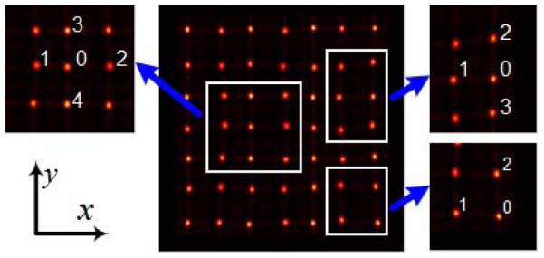
Picture illustrates an inner, edge and corner crystal and its neighbor crystals used in calculating flood histogram quality. Each inner, edge and corner crystal has 4, 3 and 2 neighbor crystals respectively.
E. Saturation of SiPMs
SiPMs are composed of microcells, each with dimensions 10 – 100 μm, operating in Geiger mode [33]. Since the SiPM response is binary, each microcell is unable to provide the number of photons detected. If a microcell is irradiated by two or more photons simultaneously, the resulting current pulse has the same amplitude and duration as that of a single photon. Due to the limited number of microcells and the required recovery time of the SiPMs (210 ns for the SiPMs used in this paper), the dynamic range of SiPMs is typically smaller compared to APDs and PMTs, and linearity of the SiPM response to light intensity is only maintained when the number of optical photons is much less than the number of microcells and the microcells are fully charged [42-43]. When this is not the case, the SiPM signal becomes disproportional to the number of optical photons because some optical photons that would otherwise be detected are incident on microcells that have fired and are not fully charged. This saturation effect will cause a compression of the energy spectrum resulting in artificially good energy resolution and will also degrade the flood histogram [44].
The saturation of the 8 × 8 SiPM array was studied by comparing the linearity of photopeak positions obtained with 511 keV photons from a 68Ge source and 662 keV photons from a 137Cs source. In the absence of saturation, the ratio of the two photopeak positions should be 511/662 = 0.77.
F. Energy resolution
Energy spectra were extracted for individual crystals in the array. The energy resolution for each crystal was found by calculating the FWHM of a Gaussian fit to the photopeak and normalizing to the 511 keV photopeak position. Average and standard deviation energy resolution were calculated using all crystals in each array.
G. Timing resolution
The timing resolution was measured by operating the detector module in coincidence with a reference detector, consisting of a single 6 × 6 mm2 MicroFB SiPM and a polished 5 × 5 × 5 mm3 LYSO crystal wrapped with Teflon tape. The coincidence timing resolution (CTRSiPM-SiPM) of two identical reference detectors was 307 ± 10 ps and 326 ± 11 ps at 5 °C and 20 °C respectively. The timing resolution was obtained by reading out the fast outputs.
Timing spectra were extracted for each individual crystal in the crystal arrays by segmenting the event data according to crystal number using a crystal look up table. The FWHM of a Gaussian fit to the timing spectra was used to estimate timing resolution.
The estimated coincidence timing resolution (CTR) of two 8 × 8 SiPM array based detectors was calculated by subtracting in quadrature the contribution of the reference detector using the following equation:
| (4) |
A CFD was used to generate time-stamps for the 8 × 8 SiPM detector module while a leading edge discriminator (LED) was used to generate time-stamps for the reference detector. Due to the time-walk of the LED method, a 506 - 516 keV energy window was applied to the reference detector to select events. Average and standard deviation timing resolution was calculated using all crystals in the array.
III. Results
A. Signal pulse shape
The signal pulse shapes from the timing channel and one of the four position channels (channel X+) are shown in Fig. 4. The red lines were obtained by coupling the 15 × 15 LYSO array to the center of the SiPM array, and the blue lines were obtained by coupling a single 3.34 × 3.34 × 20 mm3 LYSO crystal to the center of one SiPM pixel in the SiPM array. The signal pulse shapes from both the fast output and standard output for a single 3.34 × 3.34 × 20 mm3 LYSO crystal coupled to an individual 6 × 6 mm2 SiPM (MicroFB-SMTPA- 60035) are also shown in Fig. 4 (black lines).
Fig. 4.
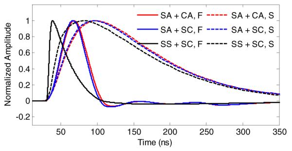
Signal shape from fast and standard outputs from a single SiPM and the 8 × 8 SiPM array. For the SiPM array, the fast and standard signal shape are the sum of all 64 signals. (Abbreviations: SA: SiPM array; SS: Single SiPM; CA: LYSO crystal array; SC: single LYSO crystal; F: fast output; S: standard output).
The pulse shapes for each configuration were the average of 200 pulses captured with an oscilloscope (DPO7254, Tektronix, Inc.), obtained at a bias voltage of 28.0 V and temperature of 5 °C. To generate the pulse shapes shown in Fig. 4, the amplitudes of the 200 pulses corresponding to a particular case were first individually normalized and then summed and averaged to give an average pulse.
Table II details the measured average signal rise time (10% - 90%) for each configuration given in Fig. 4. As shown in Fig. 4 and Table II, the signal rise time obtained with the SiPM array was slower than that obtained with the individual SiPM. Along with this, the signal rise time obtained with the 15 × 15 LYSO array coupled to the SiPM array was slightly slower than that obtained with a single LYSO crystal coupled to the center of one SiPM pixel in the SiPM array, mainly due to the different response times of the SiPMs and the combination of capacitance and noise of all the SiPMs [45]. In all cases, the fast output has a faster rise time than the standard output, hence it is better suited for timing measurements. The rise time did not show any significant improvement when the temperature was decreased from 20 °C to 5 °C (Table II).
TABLE II.
Signal rise time (10%-90%)
| Case | Signal type | Rise time / ns | |
|---|---|---|---|
| 5 °C | 20 °C | ||
| SiPM Array + LYSO Array (SA + CA) |
Fast | 23.1 ± 0.6 | 23.1 ± 0.6 |
| Standard | 38.8 ± 1.4 | 38.6 ± 1.3 | |
| SiPM Array + Single LYSO (SA + SC) |
Fast | 22.2 ± 0.4 | 22.3 ± 0.5 |
| Standard | 36.7 ± 1.1 | 36.9 ± 1.1 | |
| Single SiPM + Single LYSO (SS + SC) |
Fast | 4.5 ± 0.3 | 4.7 ± 0.4 |
| Standard | 20.9 ± 1.2 | 21.8 ± 1.2 | |
B. Noise
Fig. 5 shows the noise versus bias voltage (Fig. 5 (a)) and ovevoltage (Fig. 5(b)). The measured results include all noise sources, including the front-end board, NIM modules and PowerDAQ board. The noise of the front-end board, NIM modules and PowerDAQ board was ~ 9 ADC channels, which was a constant value during all experiments. The noise increases with increasing bias voltage and increasing temperature, mainly due to the increased spontaneous Geiger discharge probability. The noise obtained with the crystal array present was also higher, possibly due to photons from the SiPM breakdown coupling into the scintillator and reflecting back into the SiPM again, or scintillation photons generated by the Lu-176 background within the crystal array, or by cosmic.
Fig. 5.

Noise versus (a) bias voltage and (b) ovevoltage, (c) SNR versus bias
The signal-to-noise ratio (SNR), calculated as the ratio of the 511 keV photopeak amplitude to the noise, is shown in Fig. 5(c) [21]. The SNR first increases and then decreases with increasing bias voltage. The best SNR was obtained at a bias voltage of 28.5 V in all cases.
C. Flood histogram
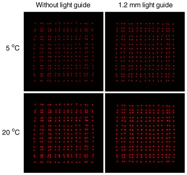
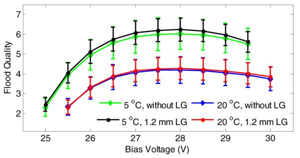
Fig. 6 shows the flood histograms of the 15 × 15 LYSO array (3.34 mm pitch) placed in the center of the SiPM sensitive area and obtained at a bias voltage of 28.0 V (the optimal bias voltage for flood histogram quality, see Fig .7). A 425 - 650 keV energy window was applied to each crystal to select events. All the crystals in the array can be clearly identified. The dependence of flood histogram quality on bias voltage is illustrated in Fig. 7. Improved flood histograms can be obtained at lower temperatures, as the SiPM noise is decreased. A light guide provides modest improvement of the average flood histogram quality value, however, the standard deviation is significantly reduced indicating that spots are overall better separated and more evenly distributed.
Fig. 6.
Flood histogram of the 15 × 15 LYSO array, obtained at a bias voltage of 28.0 V. A 425 - 650 keV energy window was applied to data from each crystal to select events.
Fig. 7.
Flood histogram quality metric versus bias voltage and temperature, obtained using the 15 × 15 LYSO array.
The flood histogram quality first increases and then decreases with increasing bias voltage. The decrease at higher bias voltage is because the noise increases quite quickly with increasing bias voltage as shown in Fig. 5(a). The best flood histogram quality was obtained at a bias voltage of 28.0 V, however the value was quite consistent between bias voltages of 27 and 29 V.
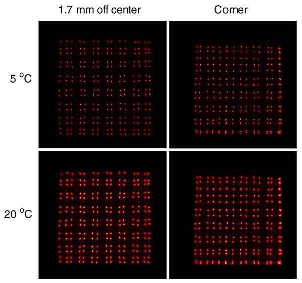
The size of the 15 × 15 LYSO array (51.0 × 51.0 mm2) is smaller than that of SiPM array (57.4 × 57.4 mm2). To further investigate the effective detection area of the SiPM array, the LYSO array was placed at two off-center positions: 1) the center of LYSO array was located 1.7 mm off the away from the center of the SiPM array in both x and y directions to mimic a 16 × 16 LYSO array; 2) the corner of the LYSO array was placed over one corner of the SiPM array to mimic an LYSO array covering the whole surface of the SiPM array. The flood histograms obtained for these two configurations are shown in Fig. 8. They were obtained at a bias voltage of 28.0 V using the 1.2 mm thick light guide.
Fig. 8.
Flood histograms of the 15 × 15 LYSO array, obtained at a bias voltage of 28.0 V and using a 1.2 mm thick light guide. A 425 - 650 keV energy window was applied to data from each crystal to select events.
When the LYSO array was coupled 1.7 mm off-center (the distance of the outermost crystal to the edge of the active area of SiPM array was 1.06 mm), all the crystals could be clearly identified. The crystal spots appeared grouped into 2 × 2 crystals, due to the relative position of the crystals with respect to the SiPM layout.
When a corner of the LYSO array was coupled to one corner of the SiPM array, the two outer rows/columns of crystals could not be resolved. These two rows/columns of crystals are almost entirely coupled to the same row/column of SiPMs, hence it is difficult to separate them, as there is very limited light sharing. A slotted light guide may help to resolve the outer crystals and will be studied in future work.
D. Saturation of SiPMs
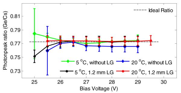
The average ratio of 511 keV to 662 keV photopeak positions for the 15 × 15 LYSO array is shown in Fig. 9. The ideal ratio, 0.772, is also plotted (gray dashed line). This ratio did not increase with increasing bias voltage, indicating that saturation was not observed up to 29.5 V in our measurements. This is because there is sufficient light sharing within the crystal array and between SiPMs (both with and without a light guide) such that the light is not concentrated on a single SiPM element.
Fig. 9.
Average ratio of photopeak positions versus bias voltage, obtained using 68Ge and 137Cs sources.
The results at higher bias voltages were not studied, as this was above the best working conditions of 28.0 V, and the signals amplitude was sufficient to saturate the electronics.
E. Crystal identification with smaller crystals
Flood histograms of crystal arrays with pitch sizes 1.5, 1.35 and 1.2 mm are shown in Fig. 10. These results were obtained at a bias voltage of 28.0 V and the crystal arrays were coupled to the center of SiPM array sequentially. A 250 - 650 keV energy window was applied to each crystal to select events. All the crystals in the LYSO arrays can be resolved except for some crystals in the 10 × 10 LSO array (1.2 mm pitch size) when the temperature is at 20 °C.
Fig. 10.
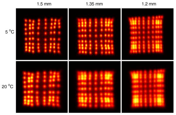
Flood histograms versus crystal pitch size and temperature obtained at a bias voltage of 28.0 V. The flood histograms were better at lower temperature. A 250 - 650 keV energy window was applied to each crystal to select events.
The corresponding flood histogram quality for each crystal array is shown in Fig. 11.
Fig. 11.
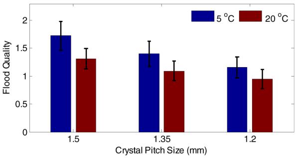
Flood quality versus crystal pitch size and temperature, obtained at a bias voltage of 28.0 V.
F. Energy resolution
The energy spectra from four representative crystals in the 15 × 15 LYSO array are given in Fig. 12(a). They were generated using single events, obtained at a bias voltage of 28.0 V and using the 1.2 mm thick light guide. The amplitude of the 511 keV photopeak is crystal-dependent, due to the 1.2 mm dead space between SiPMs. The energy spectrum of the central crystal (#113, black line) has the lowest photopeak position, as it was located over the gap of four SiPMs leading to significant light loss.
Fig. 12.

(a) Energy spectra of crystals 1, 65, 106 and 113 in the 15 × 15 LYSO array. The bias voltage was 28.0 V and data recorded at a temperature of 5 °C. A 1.2 mm thick light guide was used. (b) Average energy resolution versus bias voltage for all crystals in the 15 × 15 LYSO array. Results both with and without a 1.2 mm thick light guide (LG) are shown.
The average energy resolution across the 15 × 15 LYSO array versus bias voltage is shown in Fig. 12(b). The average energy resolution improves as the bias voltage increases and there is a tendency towards better energy resolution when the 1.2 mm light guide is used. The average energy resolution was 12.7 ± 0.8% at a bias voltage of 28.0 V (the optimal bias voltage for flood histogram quality, Fig. 7), at a temperature of 5 °C, and using the 1.2 mm light guide.
Fig. 13 shows the average energy resolution obtained for different crystal pitch sizes. Better energy resolution is obtained at lower temperature. The energy resolution values obtained with arrays with smaller pitch size is worse than with the 15 × 15 LYSO array, as light loss is increased for smaller crystal cross-sections [46].
Fig. 13.
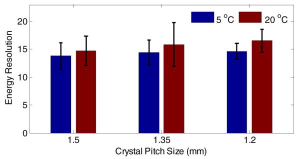
Average energy resolution versus crystal pitch size and temperature.
G. Timing resolution
Fig. 14(a) shows measured coincidence timing spectra for several crystals in the 15 × 15 LYSO array, obtained at a bias voltage of 28.0 V and temperature of 5 °C. A 425 - 650 keV energy window was applied to each crystal to select events.
Fig. 14.

(a) Timing spectra of crystals 1, 65, 106 and 113 in the 15 × 15 LYSO array at a bias voltage of 28.0 V and temperature of 5 °C , using a 1.2 mm thick light guide. (b) Average (all crystals) CTR versus temperature for the 15 × 15 LYSO array.
Fig. 14(b) shows the average estimated CTR for all crystals in the 15 × 15 LYSO array, obtained at a bias voltage of 28.0 V. Superior timing resolution is observed at lower temperature. Use of a light guide does not affect average timing resolution but increases uniformity (lower standard deviation) within the array. Using the 1.2 mm thick light guide, CTR was 1.58 ± 0.13 ns and 2.29 ± 0.26 ns, obtained at temperatures of 5 °C and 20 °C, respectively.
Fig. 15 shows the average CTR obtained using crystal arrays with different pitch sizes. A 250 - 650 keV energy window was applied to each crystal to select events. Arrays with larger crystal sizes showed superior timing resolution, consistent with the energy resolution results (Fig. 13).
Fig. 15.
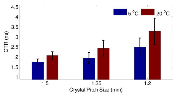
Average CTR versus crystal pitch size. Results were obtained at a bias voltage of 28.0 V.
IV. Discussion and Future work
The performance of an 8 × 8 SiPM array of 6 mm × 6 mm pixels (57.4 × 57.4 mm2 area) was characterized in detail with a view to its use as a PET detector. Flood histogram quality, energy resolution and timing resolution were studied with LYSO/LSO crystal arrays with different pitch sizes (ranging from 1.2 mm to 3.34 mm). The effect of bias voltage and operating temperature was investigated. The same trends in SNR and flood histogram quality versus bias voltage were observed for all four crystal arrays tested. The results show that varying temperature has a significant effect on the performance of these SiPMs, mainly by affecting noise characteristics. Better performance was achieved at lower temperature, as the dark count rate (noise) is lower (Fig. 5). An optimized light guide also improved the performance, especially improving the flood histogram quality and homogeneity (Figs. 6 and 7).
The best working bias voltage for this device was 28.0 V based on the flood histogram quality results measured with the 15 × 15 array of 3.34 × 3.34 × 20 mm3 LYSO crystals. The flood histogram results also showed that all crystals could be resolved in an array with a pitch size of 1.2 mm, suggesting the capability of this SiPM array for high-resolution small animal PET, and dedicated scanners for breast and brain imaging. The average energy resolution at 5 °C and at a bias voltage of 28.0 V ranged from 12.7 ± 0.8% (3.4 mm pitch crystal array) to 14.6 ± 1.4% (1.2 mm pitch array). The results we obtained are consistent with those shown in Ref. [9], which were obtained using an array of 6 × 6 mm2 SiPMs with a pitch size of 6.5 mm.
The CTR was 1.58 ± 0.13 ns, obtained at a bias voltage of 28.0 V and a temperature of 5 °C, using the 15 × 15 array of 3.34 × 3.34 × 20 mm3 LYSO crystals. The timing resolution degraded to 2.50 ± 0.44 ns for a 10 × 10 array of 1.13 × 1.13 × 14 mm3 LSO crystals. The timing resolution may be improved by optimizing the bias voltage. However, in this study the bias voltage was set to optimize flood histogram quality. The timing resolutions are similar or better compared with other recent work using large-area SiPM array and similar readout methods [9], [32]. The timing resolution results indicate the current detector modules are not suitable for time-of-flight (TOF) PET. When all the 64 fast outputs are combined together, the signal rise time was slower than that obtained with a single SiPM pixel (Fig. 4). Factors such as a combination of SiPM capacitance and noise contributed to the worse timing resolution. Better timing resolution could therefore be obtained by reducing the combined number of SiPMs and reading out more timing channels [13], [47].
During our experiments, we found that good energy resolution could also be obtained when the fast output is used to estimate the deposited energy. Fig. 16 shows a comparison of energy spectra from the standard and fast outputs. The energy spectra were generated from coincidence events by coupling a 3.34 × 3.43 × 20 mm3 LYSO crystal to a single 6 × 6 mm2 SiPM pixel. The energy resolution at 511 keV obtained from the standard output was 8.4 ± 0.1% while the fast output yielded an energy resolution of 9.2 ± 0.3 %.
Fig. 16.
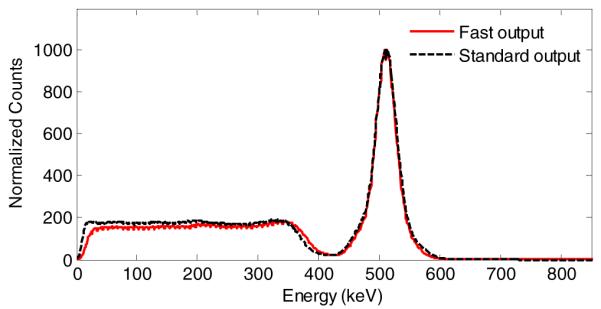
Comparison of energy spectra measured from the fast output and standard output using one single 6 × 6 mm2 SiPM and 3.34 × 3.34 × 20 mm3 LYSO wrapped with several layers of Teflon. The bias voltage was 28.0 V and the temperature was 5 °C . The energy resolution was 9.2 ± 0.3 % (fast output) and 8.5 ± 0.1 % (standard output) without saturation correction.
In the future, we plan to read out only the fast output which will be used for both timing and energy information. Each fast output will be amplified individually and timing information will be recorded for each fast output signal individually. This will isolate the SiPMs and should yield timing resolution comparable to that from individual SiPMs (<400 ps) [37-38]. However, application-specific integrated circuit (ASIC) based multi-channel electronics will be required. ASICs specifically designed for radiation detector, such as PETsys TOF PET ASIC (PETsys Electronics, Inc.) and RENA-3 (NOVA R&D Inc.) will be investigated.
A Schottky diode readout method is also under investigation by SensL [48]. In this method, the fast outputs were connected together using a Schottky diode pair per SiPM. CTRs of 304 ± 5 ps, 371 ± 4 ps and 480 ± 7 ps were obtained by combining 16, 32 and 64 MicroFB SiPMs (3 × 3 mm2 devices) together, respectively.
V. Conclusion
We have evaluated the performance of large-area SiPM array based PET detectors suitable for different PET applications. Custom front-end readout and multiplexing electronics were developed with five output electronic channels (four for event positioning and one for timing) to readout all the 128 SiPM signals (64 standard out and 64 fast outputs). A crystal array with a pitch size of 1.2 mm was resolved, and the energy resolution was less than 15% for all scintillator arrays tested. The results demonstrated the 8 × 8 array of 6 × 6 mm2 SiPMs with an area of 57.4 × 57.4 mm2 has potential for use for both human and small-animal PET scanners.
Both arrays with a pitch size of 1.35 mm and 1.2 mm were barely resolved using the five-channel readout method, however, we believe better results could be achieved using more channel-intensive readout methods, such as reading out each SiPM signal individually. In comparing the flood map quality between the two arrays, the different aspect ratios and therefore light collection efficiency of the arrays must also be considered.
We believe better performance than that shown in this paper can be obtained by further lowering the temperature to reduce noise [11], [22]. However, it is more complex to maintain a low temperature as careful consideration of moisture and the working range of electronics is needed.
New SiPMs with lower noise, such as MicroFC SiPMs have been recently developed by SensL. The noise of MicroFC SiPM is ~20% of that of MicroFB SiPMs [31]. Better performance could therefore also be expected from large-area SiPM array based on MicroFC SiPMs and studies with these devices are planned.
Acknowledgments
This work was supported in part by NIH grants R01 CA134632 and R01 EB00993.
Contributor Information
Junwei Du, Department of Biomedical Engineering, University of California, Davis, CA 95616 USA.
Yongfeng Yang, Department of Biomedical Engineering, University of California, Davis, CA 95616 USA.
Xiaowei Bai, Department of Biomedical Engineering, University of California, Davis, CA 95616 USA.
Martin S. Judenhofer, Department of Biomedical Engineering, University of California, Davis, CA 95616 USA.
Eric Berg, Department of Biomedical Engineering, University of California, Davis, CA 95616 USA.
Kun Di, Department of Biomedical Engineering, University of California, Davis, CA 95616 USA.
Steve Buckley, SensL Technologies Ltd., 6800 Airport Business Park, Cork, Ireland..
Carl Jackson, SensL Technologies Ltd., 6800 Airport Business Park, Cork, Ireland..
Simon R. Cherry, Department of Biomedical Engineering, University of California, Davis, CA 95616 USA.
REFERENCES
- [1].Roncali E, Cherry SR. Application of silicon photomultipliers to positron emission tomography. Ann. Biomed. Eng. 2011 Apr.39(no.4):1358–1377. doi: 10.1007/s10439-011-0266-9. [DOI] [PMC free article] [PubMed] [Google Scholar]
- [2].Zaidi H, Del Guerra A. An outlook on future design of hybrid PET/MRI systems. Med. Phys. 2011 Oct.38(no.10):5667–5689. doi: 10.1118/1.3633909. [DOI] [PubMed] [Google Scholar]
- [3].Wehr H, Sauter A, Divine M, Pichler BJ. Combined PET/MR: a technology becomes mature. J. Nucl. Med. 2015 Feb.56(no.2):165–168. doi: 10.2967/jnumed.114.150318. [DOI] [PubMed] [Google Scholar]
- [4].Espana S, Tapias G, Fraile L, Herraiz J, Vicente E, Udias J, Desco M, Vaquero JJ. Performance evaluation of SiPM detectors for PET imaging in the presence of magnetic fields. IEEE Nuclear Science Symp. Medical Imaging Conf. Rec..2008. pp. 3591–3595. [Google Scholar]
- [5].Yoon H, Ko G, Kwon S, Lee C, Ito M, Song I, Lee D, Hong S, Lee JS. Initial results of simultaneous PET/MRI experiments with an MRI-compatible silicon photomultiplier PET scanner. J. Nucl. Med. 2012 Apr.53(no.4):608–614. doi: 10.2967/jnumed.111.097501. [DOI] [PubMed] [Google Scholar]
- [6].Weissler B, Gebhardt P, Lerche CW, Wehner J, Solf T, Goldschmidt B, Mackewn J, Marsden P, Kiessling F, Perkuhn M, Heberling D, Schulz V. MR compatibility aspects of a silicon photomultiplier-based PET/RF insert with integrated digitisation. Phys. Med. Biol. 2014 Sep.59:5119–5139. doi: 10.1088/0031-9155/59/17/5119. [DOI] [PubMed] [Google Scholar]
- [7].Yamamoto S, Imaizumi M, Watabe T, Watabe H, Kanai Y, Shimosegawa E, Hatazawa J. Development of a Si-PM-based highresolution PET system for small animals. Phys. Med. Biol. 2010 Sep.56:5817–5831. doi: 10.1088/0031-9155/55/19/013. [DOI] [PubMed] [Google Scholar]
- [8].Isobe T, Yamada R, Shimizu K, Saito A, Ote K, Sakai K, Moriya T, Yamauchi H, Omura T, Watanabe M. Development of a new brain PET scanner based on single event data acquisition. IEEE Nuclear Science Symp. Medical Imaging Conf. Rec..2013. pp. 3540–3543. [Google Scholar]
- [9].Stolin A, Majewski S, Jaliparthi G, Raylman R, Proffitt J. Evaluation of imaging modules based on SensL array SB-8 for nuclear medicine applications. IEEE Trans. Nucl. Sci. 2014 Oct.61(no.5):2433–2438. [Google Scholar]
- [10].Shao Y, Sun X, Lan K, Bircher C, Lou K, Deng Z. Development of a prototype PET scanner with depth-of-interaction measurement using solid-state photomultiplier arrays and parallel readout electronics. Phys. Med. Biol. 2014 Feb.59:1223–1238. doi: 10.1088/0031-9155/59/5/1223. [DOI] [PMC free article] [PubMed] [Google Scholar]
- [11].Du J, Schmall J, Yang Y, Di K, Roncali E, Buckley S, Jackson C, Cherry SR. Evaluation of Matrix9 silicon photomultiplier array for small-animal PET. Med. Phys. 2015 Feb.42(no.2):585–599. doi: 10.1118/1.4905088. [DOI] [PMC free article] [PubMed] [Google Scholar]
- [12].Kim CL, McDaniel D, Ganin A. Time-of-flight PET detector based on multi-pixel photon counter and its challenges. IEEE Trans. Nucl. Sci. 2011 Feb.58:3–8. [Google Scholar]
- [13].Adachi S, Nakamura S, Hirayanagi M, Suzuki H, Uchiyama T, Baba1 T, Watanabe M, Omura T. Development of MPPC array module. IEEE Nuclear Science Symp. Medical Imaging Conf. Rec..2013. pp. 1–3. [Google Scholar]
- [14].Adachi S, Nakamura S, Hirayanagi M, Matsumoto T, Baba T, Kato T, Hayatsu K, Okuwa Y, Ota R. Development of a PET detector module. IEEE Nuclear Science Symp. Medical Imaging Conf. Rec..2014. pp. 1–3. [Google Scholar]
- [15].Liu C, Goertzen A. Multiplexing approaches for a 12 × 4 array of silicon photomultipliers. IEEE Trans. Nucl. Sci. 2014 Feb.61(no.1):35–43. [Google Scholar]
- [16].González A, Majewski S, Barberá J, Conde P, Correcher C, Hernández L, Morera C, Vidal L, Sánchez F, Stolin S, Benlloch J. Performance study of a wide-area SiPM array, ASICs controlled. IEEE Trans. Nucl. Sci. 2015 Feb.62(no.1):19–26. [Google Scholar]
- [17].Song T, Wu H, Komarov S, Siegel S, Tai YC. A sub-millimeter resolution PET detector module using a multi-pixel photon counter array. Phys. Med. Biol. 2010 May;55(no.9):2573–2587. doi: 10.1088/0031-9155/55/9/010. [DOI] [PMC free article] [PubMed] [Google Scholar]
- [18].Yamamoto S, Yeom J, Kamada K, Endo T, Levin CS. Development of an ultrahigh resolution block detector based on 0.4 mm pixel Ce:GAGG scintillators and a silicon photomultiplier array. IEEE Trans. Nucl. Sci. 2013 Dec.60(no.6):4582–4587. [Google Scholar]
- [19].McClish M, Dokhale P, Christian J, Stapels C, Johnson E, Robertson R, Shah KS. Performance measurements of CMOS position sensitive solid-state photomultipliers. IEEE Trans. Nucl. Sci. 2010 Aug.57(no.4):2280–2286. [Google Scholar]
- [20].Schmall J, Du J, Yang Y, Dokhale P, McClish M, Shah K, Cherry SR. Comparison of large-area position-sensitive solid-state photomultipliers for small animal PET. Phys. Med. Biol. 2012 Dec.57(no.24):8119–8134. doi: 10.1088/0031-9155/57/24/8119. [DOI] [PubMed] [Google Scholar]
- [21].Du J, Schmall J, Yang Y, Di K, Dokhale P, Shah K, Cherry SR. A simple capacitive charge-division readout for position-sensitive solid-state photomultiplier array. IEEE Trans. Nucl. Sci. 2013 Oct.60(no.5):3188–3197. doi: 10.1109/TNS.2013.2275012. [DOI] [PMC free article] [PubMed] [Google Scholar]
- [22].Du J, Yang Y, Berg E, Bai X, Gola A, Ferri A, Zorzi N, Piemonte C, Cherry SR. Evaluation of linearly-graded SiPMs for high resolution small-animal PET. Bio. Phys. & Eng. Express. (accepted) [Google Scholar]
- [23].Schmall J, Du J, Judenhofer M, Dokhale P, Christian J, McClish M, Shah K, Cherry SR. A study of position-sensitive solid-state photomultiplier signal properties. IEEE Trans. Nucl. Sci. 2014 Jun.61(no.3):1074–1083. doi: 10.1109/TNS.2014.2302635. [DOI] [PMC free article] [PubMed] [Google Scholar]
- [24].Rouze NC, Schmand M, Siegel S, Hutchins GD. Design of a small animal PET imaging system with 1 microliter volume resolution. IEEE Trans. Nucl. Sci. 2004 Jun.51(no.3):757–763. [Google Scholar]
- [25].Ito M, Lee J, Kwon S, Lee G, Hong B, Lee K, Sim K, Lee S, Rhee J, Hong SJ. A four-layer DOI detector with a relative offset for use in an animal PET system. IEEE Trans. Nucl. Sci. 2010 Jun.57(no.3):976–981. [Google Scholar]
- [26].Zhang H, Vu T, Bao Q, Silverman R, Berry-Pusey B, Douraghy A, Williams A, Rannou F, Stout D, Chatziioannou A. Performance characteristics of BGO detectors for a low cost preclinical PET scanner. IEEE Trans. Nucl. Sci. 2010 Jun.57(no.3):1038–1044. doi: 10.1109/TNS.2010.2046753. [DOI] [PMC free article] [PubMed] [Google Scholar]
- [27].Szanda I, Mackewn J, Patay G, Major P, Sunassee K, Mullen G, Nemeth G, Haemisch Y, Blower P, Marsden PK. National electrical manufacturers association NU-4 performance evaluation of the PET component of the NanoPET/CT preclinical PET/CT scanner. J. Nucl. Med. 2011 Oct.52(no.11):1741–1747. doi: 10.2967/jnumed.111.088260. [DOI] [PubMed] [Google Scholar]
- [28].Shao Y, Cherry SR, Farahni K, Slates R, Silverman RW, Meadors K, Bowery A, Siegel S. Development of a PET detector system compatible with MRI/NMR systems. IEEE Trans. Nucl. Sci. 1997 Jun.44(no.3):1167–1171. [Google Scholar]
- [29].Yamamoto S, Watabe H, Kanai Y, Watabe T, Aoki M, Sugiyama E, Kato K, Hatazawa J. Development of a flexible optical fiber based high resolution integrated PET/MRI system. Med. Phys. 2012 Nov.39(no.11):6660–6671. doi: 10.1118/1.4757911. [DOI] [PubMed] [Google Scholar]
- [30].Serra N, Ferri A, Gola A, Pro T, Tarolli A, Zorzi N, Piemonte C. Characterization of new FBK SiPM technology for visible light detection. JINST. 2013 Mar.8:P03019. [Google Scholar]
- [31].O’Neill K, Jackson C. SensL B-Series and C-Series silicon photomultipliers for time-of-flight positron emission. Nucl. Instrum. Methods Phys. Res. A. 2015 Jul.787:169–172. [Google Scholar]
- [32].Raylman R, Stolin A, Majewski S, Proffitt J. A large area, silicon photomultiplier-based PET detector module. Nucl. Instrum. Methods Phys.Res. A. 2014 Jan.735:602–609. doi: 10.1016/j.nima.2013.10.008. [DOI] [PMC free article] [PubMed] [Google Scholar]
- [33].Jackson C, O’Neill K, Wall L, McGarvey B. High volume SiPM production, performance and reliability. Opt. Eng. 2014 Aug.53(no.8):081909. [Google Scholar]
- [34].Du J, Schmall J, Di K, Yang Y, Judenhofer M, Bec J, Buckley S, Jackson C, Cherry SR. Design and optimization of a high-resolution PET detector module for small-animal PET based on a 12 × 12 silicon photomultiplier array. Bio. Phys. & Eng. Express. 2015 Nov.1(no.4):045003. [Google Scholar]
- [35].Saoudi A, Pepin C, Pékpin C, Houde D, Lecomte R. Scintillation light emission studies of LSO scintillators. IEEE Trans. Nucl. Sci. 1999 Dec.46(no.6):1925–1928. [Google Scholar]
- [36].Du J, Wang Y, Zhang L, Zhou Z, Xu Z, Wang X. Physical properties of LYSO scintillator for NN-PET detectors. BMEI. 2009 Oct.1:314–318. [Google Scholar]
- [37].O’Neill K, Pavlov N, Dolinsky S, Jackson C. SensL new fast timing silicon photomultiplier. Proceedings of Science - International Workshop on New Photon-detectors.Jun. 2012. pp. 1–7. [Google Scholar]
- [38].Yeom J, Vinke R, Pavlov N, Bellis S, Wall L, O’Neill K, Jackson C, Levin CS. Fast timing silicon photomultipliers for scintillation detectors. IEEE Phot. Tech. Let. 2013 Jul.25(no.14):1309–1312. [Google Scholar]
- [39].Popov V, Majewski S, Weisenberger AG, Wojcik R. Analog “Readout system with charge division type output. IEEE Nuclear Science Symp. Medical Imaging Conf. Rec..2001. pp. 1937–1940. [Google Scholar]
- [40].Popov V. Advanced data readout technique for multianode position sensitive photomultiplier tube applicable in radiation imaging detectors. JINST. 2011 Jan.6:C01061. [Google Scholar]
- [41].Judenhofer M, Pichler B, Cherry SR. Evaluation of high performance data acquisition boards for simultaneous sampling of fast signals from PET detectors. Phys. Med. Biol. 2005 Jan.50(no.1):29–44. doi: 10.1088/0031-9155/50/1/003. [DOI] [PubMed] [Google Scholar]
- [42].Gruber L, Brunner SE, Marton J, Suzuki K. Over saturation behavior of SiPMs at high photon exposure. Nucl. Instrum. Methods Phys.Res. A. 2014 Feb.737:11–18. [Google Scholar]
- [43].Vinogradov S, Arodzero A, Lanza RC, Welsch CP. SiPM response to long and intense light pulses. Nucl. Instrum. Methods Phys.Res. A. 2015 Jul.787:148–152. [Google Scholar]
- [44].Schmall J, Wiener R, Surti S, Ferri A, Gola A, Tarolli A, Piemonte C, Karp JS. Timing and energy resolution of new near-UV SiPMs coupled to :Ce for TOF-PET. IEEE Trans. Nucl. Sci. 2014 Oct.61(no.5):2426–2432. doi: 10.1109/TNS.2014.2346579. [DOI] [PMC free article] [PubMed] [Google Scholar]
- [45].Acerbi F, Ferri A, Gola A, Cazzanelli M, Pavesi L, Zorzi N, Piemonte C. Characterization of single-photon time resolution: from single SPAD to silicon photomultiplier. IEEE Trans. Nucl. Sci. 2014 Oct.61(no.5):2678–2686. [Google Scholar]
- [46].Cherry SR, Shao Y, Tornai M, Siegel S, Ricci A, Phelps ME. Collection of scintillation light from Small BGO crystals. IEEE Trans. Nucl. Sci. 1995 Aug.42(no.4):1058–1063. [Google Scholar]
- [47].Aguilar A, González A, Torres J, García-Olcina R, Martos J, Soret J, Conde P, Hernández L, Sánchez F, Benlloch J. Timing results using an FPGA-based TDC with large arrays of 144 SiPMs. IEEE Trans. Nucl. Sci. 2015 Feb.62(no.1):12–18. [Google Scholar]
- [48].Sens L. Readout methods for arrays of SiPM, application note. http://sensl.com/downloads/ds/TN-Readout_Methods_for_Arrays_of_SiPM.pdf.