

Abstract
Triboluminescence (TL) is an optical phenomenon that has a long and varied history with broad applications, such as damage detection, X-ray source, and mass health monitoring sensor. So far, the properties and mechanisms of TL remain not completely understood. The TL properties emitted during the sliding contact between Al2O3 and SiO2 surfaces were studied along different crystallographic orientations. In this study, the TL intensity of Al2O3 was significantly enhanced as Al2O3 surface was along a particular crystallographic orientation, which is an unconventional phenomenon. TL enhancement of Al2O3 was not affected by air atmosphere and atomic stocking mode of Al2O3. The enhancement mechanism of Al2O3 may be influenced by the surface state of Al2O3. This work provides a new method to control the intensity of TL and novel ideas to elucidate the TL mechanism.
Triboluminescence (TL) is a luminescence phenomenon by solid materials when they are stressed or fractured1,2. TL is also regarded as fracture, piezoelectric, and mechanical luminescence. Since the 20th century, this phenomenon has gained increasing attention because of its broad application3. TL has been successfully used in mass health monitoring sensor4, X-ray source, and damage detector5, among others. The triboluminescent properties of crystal materials are mostly investigated because many common crystal materials exhibit TL performance6.
TL properties of crystal are often affected by external factors, such as gas atmosphere, gas pressure, temperature, and speed. The photon emission intensity of Al2O3, ZrO2, and Si3N4 with a diamond stylus decreases with increasing number of carbon atoms in the hydrocarbon molecules7, whereas the emission intensity enhances to a maximum value at a particular n-butane gas pressure8. The TL intensities of NaCl and LiF doped with Br, Sr, Ca, and Pb decrease with temperature and disappear completely at 105 ± 5 and 180 ± 10 °C, respectilvely9. Hollerman et al.10 reported that the TL emission of Zn:Mn appears to be a function of speed for collision up to 6 Km/s. The doped impurities can change the TL properties of crystal materials; the TL emission intensity of ZnS:Mn is extremely strong, but TL properties are absent in ZnS4,9,11.
The physical properties of crystal structure also greatly influence TL. The discussion about TL properties of crystal with different space groups indicated that a non-centrosymmetric crystal structure is necessary but not sufficient for TL in crystal materials12,13. Hird14 reported that the intensity of TL emission during diamond polishing in ‘hard’ direction is greater than ‘soft’ direction. The crystallographic orientation of Al2O3 influences the atomic and electronic structures of alumina surfaces15. Brewer et al.16 investigated the fluorescence band at 3.0 eV, which was produced by photoexcitation in high-purity Al2O3 crystal. The results showed that the emitted light is plane polarized with the maximum intensity that occurs when the electric vector is perpendicular to the c axis of the crystal (E⊥c) and with the minimum intensity that occurs when the electric vector is parallel to the c axis (E ∥ c)16. Kurita et al.17 explored detailed atomic structures and electron states of stable and metastable surfaces of three important planes of Al2O3, namely, C plane [the (0001) surface], R plane [the ( ) surface], and A plane [the (
 ) surface]. They found that the stoichiometric surfaces of the C plane have the lowest surface energy, followed by the stoichiometric surfaces of the R plane and then the A plane. In other studies, Cs-corrected high-resolution electron microscopy that combines first-principle calculations and image simulations was used to observe and investigate the quantitative and qualitative structures of (
 ) and (0001) surfaces18. Al2O3 possesses good TL properties, but is not clearly investigated. SiO2 is a common crystal material, and the investigation of SiO2 of TL properties is very less.
The TL properties of crystal materials in different crystallographic orientations are rarely reported. We explored the TL properties of Al2O3 along different crystallographic orientations by measuring TL emission during sliding with SiO2. We discovered an unconventional phenomenon that the TL intensity was enhanced several tens of times as Al2O3 plane was in a particular crystallographic orientation. This work may provide a novel method to control the intensity of TL.
Results
TL in ambient air
Schematic diagram of light emission is shown in Fig. 1(a), the intensity of light emission of Al2O3 is greatly enhanced due to crystallographic orientation changed from ( ) to (0001). The images of photon emitted in ambient air during the sliding contact between Al2O3 (0001), (
 ), (
), ( ), and (
 ) surfaces and SiO2 (110) under normal force (F) of 10 N and relatively shear velocity (V) of 33 mm/s are shown in Fig. 1(b–e). Images of (c) and (d) are much brighter than those of (b) and (e). The mean intensities of I(b), I(c), I(d), and I(e) were 249, 1605, 4512, and 222, respectively. The mean intensities of (b) and (e) are much weaker compared with those of (c) and (d). I(c) is about 10 and 7 times higher than I(b) and I(e), and I(d) is about 22 and 14 times higher than I(b) and I(e). The images of photons emitted during sliding between Al2O3 (0001), (
 ), (
), ( ), and (
 ) surfaces and SiO2 (003) are also shown in Fig. 1. In this condition, the intensity of TL has the same appearance although crystallographic orientation of SiO2 is changed. Thus, the TL intensities of Al2O3 (
 ) and (
 ) surfaces are significantly enhanced compared with the TL intensities of Al2O3 (0001) and (
 ) surfaces.
Figure 1.

(a) Schematic of light emission of Al2O3 (0001) and ( ) surfaces, and photon images emitted under F = 10 N and V = 33 mm/s during the sliding between SiO2 (110) and (b) Al2O3 (0001) with mean intensity I(b) = 178, (c) Al2O3 (
 ) with I(c) = 1730, (d) Al2O3 (
 ) with I(d) = 3671, and (e) Al2O3 (
 ) with I(e) = 259, and during the sliding between SiO2 (003) and (f) Al2O3 (0001) surface with I(f) = 103, (g) Al2O3 (
 ) surface with I(g) = 1134, (h) Al2O3 (
 ) surface with I(h) = 2534, and (i) Al2O3 (
 ) surface with I(i) = 234.
The spectra of photons emitted in ambient air during the sliding contact between Al2O3 (0001), ( ), (
), ( ), and (
 ) surfaces and SiO2 (110) under F = 10 N and V = 33 mm/s are shown in Fig. 2(a). Many sharp peaks in regions 300–450 nm and 600–900 nm are on spectra, but the spectra intensities of diverse Al2O3 surfaces are quite different. The maximum spectra intensities of Al2O3 (
 ) and (
 ) surfaces are much higher than those of Al2O3 (0001) and (
 ) surfaces. The maximum spectrum intensity of Al2O3 (
 ) is nearly five times of spectra intensity of Al2O3 (0001) and (
 ) surfaces, in quantitative terms, while the maximum spectrum intensity of Al2O3 (
 ) is more than 10 times than those of Al2O3 (0001) and (
 ) surfaces. As the crystallographic orientation of SiO2 is changed from (110) to (003), the spectra intensities of Al2O3 (
 ) and (
 ) surfaces of Al2O are much stronger. Thus, the intensity of emission is enhanced, when Al2O3 (
 ) and (
 ) surfaces are sliding with SiO2.
Figure 2.

The spectra of photons emitted under F = 10 N and V = 33 mm/s in air: (a) during the sliding between (0001), ( ), (
), ( ), and (
 ) surfaces of Al2O3 and SiO2 (110), (b) during the sliding contact between (0001), (
 ), (
), ( ), and (
 ) surfaces of Al2O3 and SiO2 (003).
We conducted other sliding experiments to study further the enhancement mechanism of TL intensity of Al2O3. The images and spectra of photons emitted in ambient air during the sliding contact between Al2O3 (0001), ( ), (
), ( ), and (
 ) surfaces and SiO2 (110) surface under F = 10 N and V = 33 mm/s by using a wire line are shown in Fig. 3. The wire line that connects the holder and platform could reduce the external electric potential difference between Al2O3 and SiO2 to some extent. The mean intensities of images of Al2O3 (0001), (
 ), (
), ( ), and (
 ) surfaces are 92, 198, 223, and 91, respectively. The mean intensities of images of Al2O3 (
 ) and (
 ) surfaces are higher than those of Al2O3 (0001) and (
 ) surfaces. The maximum intensity of images of Al2O3 (
 ) is nearly three times stronger than those of Al2O3 (0001) and (
 ) surfaces. In this condition, the photons emitted in ambient air are extremely weaker through eliminating the effect of external electric potential difference. The spectra of photons of Al2O3 (
 ) and (
 ) surfaces have sharp peaks as shown in Fig. 3(e), whereas those of Al2O3 (0001) and (
 ) surfaces have no peaks. Thus, the TL intensities of Al2O3 (
 ) and (
 ) surfaces are much higher.
Figure 3.

Photons under F = 10 N and V = 33 mm/s using a wire line in ambient air during the sliding between SiO2 (110) and Al2O3 (0001) (a) images with I = 92 and (e) spectra, Al2O3 ( ) (b) images I = 198 and (f) spectra, Al2O3 (
 ) (c) images I = 223 and (g) spectra, Al2O3 (
 ) (d) I = 91 and (h) spectra.
TL in vacuum
To explore better the TL properties of Al2O3, we conducted subsequent experiments in vacuum instead of ambient air. Figure 4 shows the images and spectra of photons emitted during the sliding contact between Al2O3 (0001), ( ), (
), ( ), and (
 ) surfaces and SiO2 (110) in vacuum under F = 10 N and V = 33 mm/s. The spectra of Al2O3 in vacuum which are composed of instrument noise, have no characteristic peaks due to very lower photons intensity. The mean intensities of photon images of Al2O3 (
 ) and (
 ) surfaces are higher than those of Al2O3 (0001) and (
 ) surfaces. The mean intensity of Al2O3 (
 ) is nearly two times stronger than those of Al2O3 (
 ) and (
 ) surfaces.
Figure 4.

Photons under F = 10 N and V = 33 mm/s in vacuum during the sliding between SiO2 (110) and Al2O3 (0001) (a) images with I = 35 and (e) spectra, Al2O3 ( ) (b) images I = 114 and (f) spectra, Al2O3 (
 ) (c) images I = 119 and (g) spectra, Al2O3 (
 ) (d) I = 81 and (h) spectra.
The spectra of photons emitted in vacuum have no peaks because of extremely low light intensity as shown in Fig. 4(e). In this condition, the TL properties of Al2O3 are also affected by crystallographic orientation, and the TL intensities of Al2O3 ( ) and (
 ) surfaces are enhanced.
Friction and abrasion
The friction coefficients of the sliding contact between Al2O3 (0001), ( ), (
), ( ), and (
 ) surfaces and SiO2 (110) are measured using a Universal Micro-Tribotester (UMT-3; Bruker, America), where the values of friction coefficients are 0.179, 0.258, 0.261, and 0.329. The friction coefficient of Al2O3 (0001) surface is lowest and that of Al2O3 (
 ) surface is highest. The friction coefficients of Al2O3 (
 ) and (
 ) surfaces are much closer. The results prove that the TL intensity has no evident linear relationship with friction coefficient as the TL intensities of Al2O3 (
 ) and (
 ) surfaces are much higher.
The depth and width of grinding cracks on SiO2 (110) surfaces, which are sliding with Al2O3 (0001), ( ), (
), ( ), and (
 ) surfaces, are measured using a Talysurf (5P-120; Taylor Hobson, England). Figure 5 is the mean depth and width of the grinding crack of SiO2 (110) by sliding with Al2O3 (0001), (
 ), (
), ( ), and (
 ) surfaces. The values of mean depth of four groups are close to 0.02 mm, whereas those of SiO2 (110) surfaces have no distinct differences. The results stated that abrasions of SiO2 (110) surfaces sliding with Al2O3 (0001), (
 ), (
), ( ), and (
 ) surfaces have no apparent variations. Thus, the TL intensity of Al2O3 is not influenced by wear of SiO2, and enhancement mechanism of TL properties of Al2O3 is dominated by crystallographic orientation.
Figure 5. Mean depth and width of grinding crack of SiO2 (110).
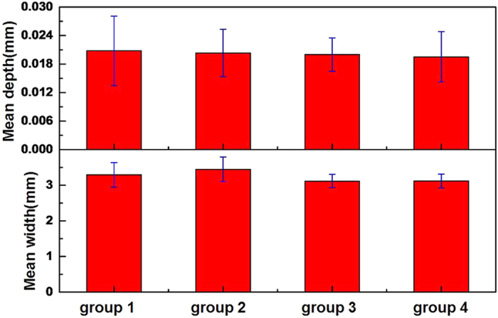
Group 1is SiO2 (110) sliding with Al2O3 (0001), group 2 is SiO2 (110) sliding with Al2O3 ( ), group 3 is SiO2 (110) sliding with Al2O3 (
 ), group 4 is SiO2 (110) sliding with Al2O3 (
 ).
).
Discussion
The Al2O3 crystal is a hexagonal crystal, and the side views of atom arrangement of Al2O3 (0001), ( ), (
), ( ), and (
 ) surfaces are shown in Fig. 6(a–d), respectively. In the hexagonal unit cell, the atoms are stacked along the [0001] direction in a sequence of an oxygen layer and Al double layers: -AlAlO3-AlAlO3-R (Fig. 6(a)). The atoms along the [
 ] direction are a layer unit that consists of five atomic layers: an O layer constructed of one O atom in the 1 × 1 unit, an O layer constructed of two O atoms, an Al layer constructed of four Al atoms, and an O layer constructed of one O atom17. This -O-O2-Al4-O2-O- repeating layer unit has no dipole moment along the [
 ] direction17. The atoms are stacked along the [
 ] direction in a sequence of an O layer and an Al layer: -O-Al-O-Al-R- (Fig. 5(b))18. The 1 × 1 lateral unit of the (
 ) surface is a layer unit in a sequence of an Al layer constructed of two Al atoms and an O layer constructed of two O atoms. The -Al2-O2-Al2-O2- repeating layer unit has no dipole moment along the direction perpendicular to the (
 ) surface18. The atomic stacking mode of Al2O3 is extremely complicated along different crystallographic orientations, where (
 ) and (
 ) Al2O3 surfaces have no similar stacking mode. No regular discipline exists to indicate that the enhancement of TL intensities of (
 ) and (
 ) Al2O3 surfaces is related to atomic stacking mode.
Figure 6.

Side view of atom arrangement of Al2O3 surfaces: (a) (0001), (b) ( ), (c) (
 ), (d) (
 ); and (e): energy levels of Al2O3 and SiO2.
The results of rough measurements of surface charge of Al2O3 and SiO2 by using faraday cup19 showed that Al2O3 surface was negatively charged and SiO2 was positively charged. Tribocharging mechanism is that electrons transferred from a surface with a low work function to a mating surface with a high work function20. In surface state theory, charge is exchanged between surface states in proportion to the difference between the effective or surface work functions of the two materials21. Surface potential difference is the fermi level difference between original surfaces as well as the work function difference22. In equation (1), VC is the surface potential difference, ϕ1, ϕ2 are the work functions of two surfaces respectively23.
 |
SiO2 surface has a lower work function than Al2O3 surface24,25. Thus, electrons are transferred from SiO2 to Al2O3, resulting in the former being positive and the latter being negative, then electric field between SiO2 and Al2O3 contacting surfaces is formed26. Electrons of ambient air molecules in electric field will be excited from ground level to the exited levels, then fall down to the lower or ground level, photons are emitted26. The sharp peaks of spectra are caused by the electrical breakdown of ambient gas27. The spectra peaks of photons in the region 300–450 nm are assigned to C3π → B3π electron transitions of N228. Other sharp peaks of spectra are mainly due to the B3π → A3Σ electron transitions of N2 and the b1Σ+g → X3Σ−g electron transition in O227. The pressure of vacuum chamber is between 1 to 10 Pa during the sliding experiment. Air molecules are much smaller under this condition. Thus, Photons emitted during sliding between SiO2 and Al2O3 in vacuum is very few, the spectra of Al2O3 in vacuum have no peaks.
As shown in Fig. 6(e), the band gap of SiO2 is 9 eV, and the conduction band (Ec) is −0.9 eV29,30. The surface states (SS) of Al2O3 (0001) and Al2O3 ( ) are 9 and 12 eV, respectively. The bottom of Fermi level of Al2O3 (
 ) is 0.8 eV31,32. Al2O3 (
 ) has two surface-state bands at 12 and 15 eV. The bottom of the Fermi level of Al2O3 (0001) is −6.8 eV, which is much lower than that of (
 ). Al2O3 (0001) has two surface-state bands at 9 and 12.5 eV. The surface states of Al2O3 (
 ) are much higher than those of Al2O3 (0001). Thus, enhancement mechanism of Al2O3 may be related to the energy levels of Al2O3, while much higher energy levels of Al2O3 (
 ) surface result in increasing TL emission.
The enhancement mechanism of TL properties of Al2O3 may be influenced by the surface state of Al2O3. The enhancement mechanisms of Al2O3 still need further exploration, and our work may provide a novel method to control the TL intensity.
Methods
Materials
SiO2 and Al2O3 crystals with trigonal and hexagonal crystal structures, respectively, were used in the sliding experiment. The two types of crystal planes of SiO2 were (110) surface by X cut and (003) surface by Z cut. The results of single-crystal X-ray diffractometer of SiO2 surfaces are shown in Fig. 7(a). Four surface planes of Al2O3 crystal, including C plane (0001), A plane ( ), M plane (
 ), and R plane (
 )33, were used as shown in Fig. 7(b). (
 ) and (
 ) planes are parallel to axis, and (0001) plane is perpendicular to axis, (
 ) plane is crossed with C axis. The dielectric constant of sapphire at 298 K in 103–109 Hz interval is ∥C = 11.5, ⊥C = 9.334. Dielectric constant of four planes of Al2O3 have little difference. The SiO2 with width of 3 mm and thickness of 2 mm and the Al2O3 with diameter of 30 mm and thickness of 2 mm were purchased from Shanghai Daheng Optics & Fine Mechanics Co. Ltd. The Vickers hardness of (110) and (003) surfaces of SiO2 are 1257 and 1167, respectively, and those of Al2O3 (0001), (
 ), (
), ( ), and (
 ) surfaces are 2060, 2119, 2076, and 2329, respectively. The roughness of (110) and (003) surfaces of SiO2 are 1.6 and 1.44 nm, respectively, and those of Al2O3 (0001), (
 ), (
), ( ), and (
 ) surfaces are 5.43, 5.21, 5.18, and 5.51 nm. In our experiments, Al2O3 (0001), (
 ), (
), ( ), and (
 ) surfaces would be slid with SiO2 (110) and (003) surfaces, respectively.
Figure 7.

(a) Single-crystal X-ray diffractometer results of Al2O3 surfaces with miller indices (0001), ( ), (
), ( ), (
), ( ), and SiO2 surfaces with miller indices (110) and (003). (b) Al2O3 planes in hexagonal unit cell.
Experimental setup
The schematic of the experiment setup used to observe the images and spectra of photons during sliding between SiO2 and Al2O3 is shown in Fig. 8. Optical fiber was used to gather light and then transmitted the light to a spectrograph (SP2500; Princeton Instruments, America). The images and spectra of photons were obtained with the spectrograph and CCD. The spectra of photons ranged from 300 nm to 900 nm, and the image of photons reflected the overall intensity of light.
Figure 8. Schematic diagram of the sliding experiment setup for observation of the images and spectra of photons.

Experimental condition
SiO2 was adhered to the rotating platform along with the motor, and the Al2O3 wafer was fixed on a holder under a normal force of 10 N, as shown in Fig. 8. The bottom surface of Al2O3 wafer was sliding over the top surface of SiO2 wafer. The integration time (T) of CCD camera was 10 min, and the relative shear velocity (V) between Al2O3 and SiO2 wafer was 33 mm/s. The sliding experiment was performed in ambient air and vacuum. The vacuum pressure was between 1 and 10 Pa, and air humidity was nearly 10%. The red line in Fig. 8 is a removable wire line. The wire line connected the holder and the platform to reduce the influence of the external electrical potential difference. Each test was run three times, and mean was obtained to remove any discrepancies. The mean intensity of photon images is calculated by summing values of bright zone then dividing numbers of pixel points.
Additional Information
How to cite this article: Wang, K. et al. Triboluminescence dominated by crystallographic orientation. Sci. Rep. 6, 26324; doi: 10.1038/srep26324 (2016).
Acknowledgments
The work was financially supported by the National Natural Science Foundation of China. (51305225,51527901), the National Key Basic Research Program of China (2013CB934200), Research Fund of the Tsinghua University (20131089320).
Footnotes
Author Contributions L.M., X.X. and S.W. conceived the experiments. K.W. conducted the experiments and processed the experimental data. L.M., X.X. and K.W. analysed the results. All authors reviewed the manuscript.
References
- Zink J. I. & Triboluminescence J. Accounts Chem Res. 11, 289–295 (1978). [Google Scholar]
- David O. O. et al. Progress in triboluminescence-based smart optical sensor system. J. Lumin. 131, 1407–1418 (2011). [Google Scholar]
- Chandra B. P. Kinetics of triboluminescence in crystals. J. Phys D: Appl Phys. 10, 1531–1538 (1977). [Google Scholar]
- Hollerman W. A. et al. Annealing effects of triboluminescence production on irradiated ZnS:Mn. J. Surf Coat Technol. 201, 8328–8387 (201). [Google Scholar]
- Olawale D. O. et al. Getting light through cementitious composites with in situ triboluminescent damage sensor. J. Struct Health Monit. 13, 177–189 (2014). [Google Scholar]
- Sweeting L. M., Triboluminescence with and without Air. J. Chem Mater. 13, 854–870 (2001). [Google Scholar]
- Nakayama K. J. & Hashimoto H. S. Triboemission of charged particles and photons from wearing ceramic surfaces in various hydrocarbon gases. J. Wear. 185, 183–188 (1995). [Google Scholar]
- Nakayama K. J. & Hashimoto H. S. Triboemission, tribochemical reaction, and friction and wear in ceramics under various n-butane gas pressures. J. Tribol Int. 29, 385–393 (29). [Google Scholar]
- Chandra B. P., Khokhar M. S. K., Elyas M. & Rao A. M. D. The effect of temperature on the triboluminescence of Ba, Sr, Ca and Pb doped NaCl and LiF single crystals. J. Phys D: Appl Phys. 23, 90–94 (1990). [Google Scholar]
- Hollerman W. A. et al. Review of Triboluminescence Impact Research at Projectile Speeds of 1 m/s to 6km/s. J. Procedia. Eng. 58, 392–400 (2013). [Google Scholar]
- Chandra V. K., Chandra B. P. & Jha P. Self-recovery of mechanoluminescence in ZnS:Cu and ZnS:Mn phosphors by trapping of drifting charge carriers. J. Appl Phys Lett. 103, 1–5 (2013). [Google Scholar]
- Sweeting L. M. et al. Crystal Structure and Triboluminescence 2. 9-Anthracenecarboxylic Acid and Its Esters. J. Chem Mater. 9, 1103–1115 (1997). [Google Scholar]
- Sweeting L. M. & Rheingold A. L. Crystal Structure and Trlbolumlnescence. 1. 9-Anthryl Carbinols. J. Phys. Chem. 92, 5648–5655 (1988). [Google Scholar]
- Hird J. R., Chakravarty A. & Walton A. J. Triboluminescence from diamond. J. Phys D: Appl Phys. 40, 1464–1472 (2007). [Google Scholar]
- Fang C. M. & Groot R. A. The nature of electron states in AlN and α-Al2O3. J. Phys.: Condens. Matter. 19, 1–6 (2007). [Google Scholar]
- Brewer J. D., Jeffries B. T. & Summers G. P. Low-temperature fluorescence in sapphire. J. Phys Rev B. 22, 4900–4906 (1980). [Google Scholar]
- Kurita T., Uchida K. & Oshiyama A. Atomic and electronic structures of α-Al2O3surfaces. J. Phys Rev B. 82, 1–14 (2010). [Google Scholar]
- Gautier M., Fenaud G., Pham Van L., Villette B., Pollak M., Thromat N. & Duraud J. P. α-Al2O3 (0001) Surfaces: Atomic and Electronic Structure. J AM Ceram Soc. 77, 323–334 (1994). [Google Scholar]
- Zhang Y. Y. & Shao T. M. A method of charge measurement for contact electrification. J. Electrostat. 71, 712–716 (2013). [Google Scholar]
- Nakayama K. J. & Nevshupa R. A. Effect of dry air pressure on characteristics and patterns of tribomicroplasma. J. Vacu. 74, 11–17 (2004). [Google Scholar]
- Castle P. S. G. Contact Charging Between Insulators. J. Electrostat. 40, 13–20 (1997). [Google Scholar]
- Lowell J. & Rose-innes A. C. Contact electrification. J. Adv Phys. 29, 947–1023 (1980). [Google Scholar]
- Lavielle L. Electric field effect on the friction of a polyethylene-terpolymer film on a steel substrate. Wear. 176, 89–93 (1994). [Google Scholar]
- Fonseca L. R. C. & Knizhnik A. A. First-principles calculation of the TiN effective work function on SiO2 and on HfO2. J. Phys Rev B. 74, 1–13 (2006). [Google Scholar]
-
Guo J., Ellis D. E. & Lam D. J.
Electronic structure and energetics of sapphire (0001) and (
 ) surfaces. J. Phys Rev B.
45, 647–656 (1997). [DOI] [PubMed] [Google Scholar]
) surfaces. J. Phys Rev B.
45, 647–656 (1997). [DOI] [PubMed] [Google Scholar] - Zink J. I. Squeezing Light out of Crystals: Trboluminescence. J. Naturwissenschaften. 10, 507–512 (1981). [Google Scholar]
- Nakayama K. J. & Nevahupa R. A. Characteristics and Pattern of Plasma Generated at Sliding Contact. J. Tribo. 125, 780–787 (125). [Google Scholar]
- Hardy G. E. & Zink J. I. Triboluminescence and Pressure Dependence of the Photoluminescence of Tetrahedral Manganese(II) Complexes. J. Inorg Chem. 12, 3061–3065 (1976). [Google Scholar]
- Markoy S. From ab initio properties of the Si-SiO2 interface, to electrical characteristics of metal-oxide-semiconductor devices. J. Phys Conf Ser. 242, 1–4 (2010). [Google Scholar]
- Geis M. W., Gregory J. A. & Pate B. B. Capacitance-Voltage Measurements on Metal-SiO2-Diamond Structures Fabricated with (100)- and (1 1 1)-Oriented Substrates. J. Ieee t electron dev. 38, 619–626 (1991). [Google Scholar]
- Minseok C., Anderson J. & Chris G. V. Native point defects and dangling bonds in α-Al2O3. J. Appl Phys. 113, 1–6 (2013). [Google Scholar]
- Nagy L. T. et al. Electronic structure of alumina surface. J. Int J Quantum Chem. 70, 341–350 (1998). [Google Scholar]
- Dobrovinskaya E. R., Lytvynov L. A. & Pishchik V. Sapphire: material, manufacturing, applications. Ch. 2, 76–78 (Spring Science & Business Media, 2009). [Google Scholar]
- Dobrovinskaya E. R., Lytvynov L. A. & Pishchik V. Sapphire: material, manufacturing, applications. Ch. 2, 115–117 (Spring Science & Business Media, 2009). [Google Scholar]