Abstract
Zigzag edges of graphene nanostructures host localized electronic states that are predicted to be spin-polarized. However, these edge states are highly susceptible to edge roughness and interaction with a supporting substrate, complicating the study of their intrinsic electronic and magnetic structure. Here, we focus on atomically precise graphene nanoribbons whose two short zigzag edges host exactly one localized electron each. Using the tip of a scanning tunnelling microscope, the graphene nanoribbons are transferred from the metallic growth substrate onto insulating islands of NaCl in order to decouple their electronic structure from the metal. The absence of charge transfer and hybridization with the substrate is confirmed by scanning tunnelling spectroscopy, which reveals a pair of occupied/unoccupied edge states. Their large energy splitting of 1.9 eV is in accordance with ab initio many-body perturbation theory calculations and reflects the dominant role of electron–electron interactions in these localized states.
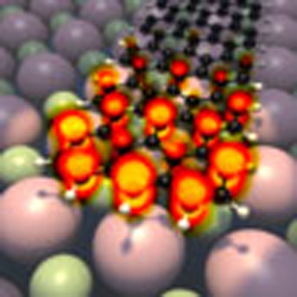 The zigzag edges of graphene host edge-localized electronic states with aligned electron spins, but these states strongly interact with metallic substrates. Here, the authors measure the electronic structure of graphene nanoribbons after transferring them to an insulating support.
Recent advances in the fabrication of precise graphene nanostructures open the door to tailoring their electronic properties to the needs of specific applications. In the case of graphene nanoribbons (GNRs) with armchair edges, a bottom-up approach has been shown to deliver control over width and edge termination down to the atomic level1. This allows for precise tuning of the electronic band gap2,3,4 and optical response5 by adjusting the shape and coupling motifs of the molecular building blocks. Even more intriguing are graphene nanostructures with zigzag edges, which are predicted to host spin-polarized edge states by different levels of theory6,7,8,9,10. Although a significant number of theoretical studies have investigated specific graphene nanostructures with zigzag edges, predicting spin filtering properties11, half-metallic behaviour12 and spin confinement13, experimental results are scarce and widely affected by limited structural precision and/or pronounced interaction with the substrate. Previous experimental studies of graphene zigzag edges have concentrated mainly on metal-adsorbed graphene nanostructures, where the low-energy edge states may interact with the nearby electron reservoir. For graphene nanoislands on Ir(111), edge states are found to be completely suppressed14. On less reactive surfaces, such as Au(111)15,16,17,18,19,20, edge states have been observed for a variety of graphene nanostructures, even at interfaces between graphene and hexagonal boron-nitride18,20. However, the reported spectroscopic features of edge states vary greatly. For example, the energy splitting between occupied and empty edge states ranges from 0 eV (ref. 17) to 0.3 eV (ref. 19). These values are much smaller than expected from electronic structure calculations for structurally perfect zigzag edges within many-body perturbation theory, which predicts a splitting of ≈1.9 eV for the most strongly localized edge state8. Indeed, a recent study of the edges of graphene grown on silicon carbide21 reports a substantial energy splitting of up to 1.2 eV, however, the edges obtained from nanoparticle-assisted etching lack atomic precision. In summary, reducing both edge roughness and substrate interaction can be considered a prerequisite for studying the intrinsic electronic and magnetic structure of graphene zigzag edges.
Here, we focus on the electronic properties of the atomically precise zigzag edges formed at the termini of bottom-up fabricated armchair graphene nanoribbons (AGNRs). To decouple their electronic structure from the metal substrate, on which they are grown, we transfer the AGNRs onto NaCl islands by a scanning tunnelling microscopy (STM)-based multistep manipulation routine. Using scanning tunnelling spectroscopy (STS), we find that electronic decoupling of the edge states establishes a large energy splitting between occupied and unoccupied edge states. This is in accordance with ab initio many-body perturbation theory calculations, which we use to systematically distinguish between edge states localized at the zigzag edges and the energetically and spatially distinct states associated with the armchair edges in the GNRs under study.
Results
Short graphene zigzag edge on a thin insulator
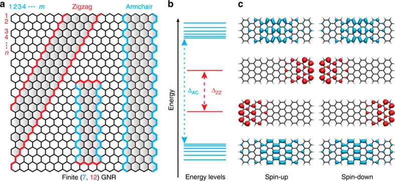
We focus on short AGNRs of width m=7, which are synthesized with atomic-scale precision on a Au(111) single crystal surface using a recently established bottom-up method1. The two armchair and two zigzag edges of the GNRs are atomically precise, monohydrogenated edges, as demonstrated by previous combined STM and atomic force microscopy studies17. Following Fig. 1a, the GNRs are denoted as (7, n) GNRs, where n specifies their length along the armchair direction in units of carbon zigzag lines. Finite (7, n) GNRs host two qualitatively different sets of electronic π-states. One set derives from the Bloch states of the bulk GNR, which are delocalized along the GNR. The short zigzag edges at the termini of the GNRs give rise to another set of states that are localized near the termini10. As sketched in Fig. 1b,c, these edge states (Tamm states22) are energetically isolated from the delocalized bulk states of the GNR, thus offering an experimental advantage over graphene nanostructures with long zigzag edges, where the energies of edge-localized and delocalized states are predicted to overlap6,8. Previous STS investigations of (7, n) GNRs on Au(111) indicated only one, possibly degenerate, edge state near the Fermi level, which may be explained by hole-doping of the GNR17. In order to characterize their intrinsic electronic structure, the GNRs thus need to be transferred to a different substrate—a process that is also required for future GNR-based applications23.
Figure 1. Electronic structure of finite graphene nanoribbons.
(a) Cutting graphene into nanoribbons with different edge topologies. Indices (m, n) are used to denote the dimensions of a graphene nanoribbon (GNR) along the zigzag (m) and armchair direction (n), respectively. (b) Sketch of energy levels for a finite (7, 12) GNR, with ΔAC and ΔZZ indicating the bulk band gap and the splitting of the localized states at the zigzag edges, respectively. (c) Kohn–Sham spin-orbitals of edge-localized states and energetically closest bulk states. Electrons with different spins are localized at opposing zigzag edges.
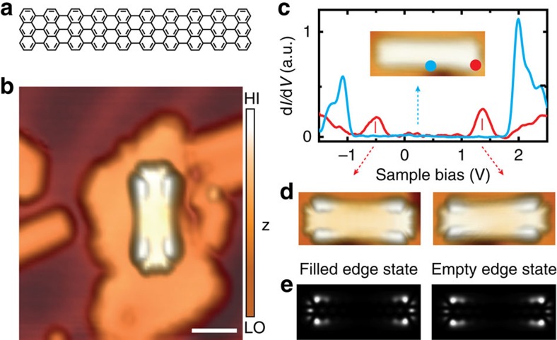
As the synthesis relies on the catalytic activity of the metal surface, the transfer onto an insulating substrate needs to occur after the synthesis. Here, we use atomically thin insulating NaCl films that are deposited directly onto the metal surface. In contrast to bulk insulators, these films still allow the electronic properties of adsorbates to be investigated by STM/STS, while considerably reducing their interaction with the metal substrate24. Through a novel four-step STM manipulation routine (see the Methods, Supplementary Fig. 1 and Supplementary Note 1), we transfer ribbons with lengths ranging from 2 to 10 nm onto a monolayer of NaCl without introducing any defects. The transfer process relies on the weak adhesion of defect-free (7, n) GNRs to the Au(111) growth substrate, which enables lateral manipulation and controlled pick-up of individual GNRs by the STM tip22. Figure 2b shows a typical STM scan of a (7, 20) GNR on NaCl. When positioning the STM tip above a zigzag end of the decoupled GNR, the differential conductance (dI/dV) spectrum exhibits two peaks centred at −0.5 and 1.3 V, as shown in Fig. 2c (see Supplementary Fig. 4 for a scan along the zigzag edge and Supplementary Fig. 5 for comparison with a reference spectrum on NaCl). Both peaks are well separated from the Fermi energy, thus excluding the possibility of (partial) charge transfer. STM images taken at these bias voltages clearly associate the peaks with electronic states localized at the zigzag-terminated ends. As shown in Fig. 2d, the shapes of filled and empty edge states are essentially identical. Their characteristic features, such as the broadening towards the very end of the GNR as well as the protrusions at the outermost carbon atoms, are in excellent agreement with the orbital densities of the corresponding states in Kohn–Sham density functional theory (DFT) calculations for freestanding GNRs, when the finite tip-sample distance is taken into account25 (cf. Fig. 2e).
Figure 2. Electronic structure of (7, 20) graphene nanoribbon on NaCl monolayer.
(a) Structural model of a (7, 20) GNR. Scale bar, 2 nm. (b) STM topography image of a (7, 20) GNR transferred onto a NaCl monolayer island through STM manipulation (U=−1.0 V, I=30 pA). Colour bar: HI=high; LO=low. (c) Differential conductance spectra measured in the centre (blue) and at a zigzag end (red) of the decoupled (7, 20) GNR. Inset: STM topography image at sample bias in the band gap of the ribbon (U=−0.5 V, I=30 pA). (d) STM topography images showing the orbital shapes of the occupied edge state (left, U=−1.0 V, I=30 pA) and the unoccupied edge state (right, U=1.4 V, I=30 pA). (e) Local density of states of corresponding Kohn–Sham orbitals at 4 Å distance above the GNR.
Theoretical treatment of edge state splitting
Being a theory of the electronic ground state, Kohn–Sham DFT is not designed to describe the charged excitations that take place in STS, which involve the addition/removal of electrons to/from the sample. Although the orbitals of the non-interacting Kohn–Sham system are often found to be accurate approximations of the corresponding quasiparticle wave functions26, the Kohn–Sham orbital energies are known to deviate significantly from quasiparticle excitation energies in many bulk insulators and molecules. In particular, the Kohn–Sham gap of standard semi-local DFT functionals (and even of the exact functional27) can severely underestimate the fundamental gap, defined as the difference between the ionization potential and the electron affinity. An accurate description of the fundamental gap needs to properly account for the interaction of the additional charge with the remaining electrons. This many-body effect of dynamical screening is captured naturally by many-body perturbation theory in the GW approximation. The framework provides accurate fundamental gaps, both for bulk insulators28 and molecules29, and has been applied successfully to GNRs of infinite length8.
Here we perform ab initio
GW calculations for finite (7, n) GNRs, which can be viewed as open-shell molecules with one, singly occupied state localized at each terminus. Their fundamental gap is given by the energy splitting ΔZZ between the occupied and empty edge-localized states. A significant Kohn–Sham gap opens only in the spin-unrestricted formalism, where breaking of spin symmetry gives rise to staggered sublattice potentials7. Using the semi-local Perdew-Burke-Ernzerhof (PBE) functional30, a Kohn–Sham gap of  is obtained for lengths n⩾12. Starting from the PBE orbitals and orbital energies, we compute quasiparticle corrections in the G0W0 approximation. The fundamental gap ΔZZ is found to converge rapidly as a function of length, yielding a value of
  =2.8±0.1 eV for n⩾12 (see Fig. 3g for details), exceeding the Kohn–Sham gap by more than a factor of five. Note also that
  is larger than the G0W0 gap of maximum 1.9 eV between states localized at extended zigzag edges8, as expected from the additional confinement along the zigzag direction (see Supplementary Fig. 2 and Supplementary Note 2 for the link between the edge state of the (7, n) GNR and the edge states of extended zigzag edges). Direct comparison to experiment would require the inclusion of dynamical screening not only by the electrons of the GNR itself, but also by those of the NaCl monolayer and the underlying Au substrate, which is expected to lead to significant reduction of the fundamental gap2. Owing to computational constraints, we do not describe screening by the substrate quantitatively here (see refs 2, 31 for studies modelling such effects), but point out that the experimentally observed gap of ΔZZ=1.9 eV is fully compatible with a fundamental gap of 2.8 eV, reduced by screening from substrate electrons.
Figure 3. Length-dependent electronic structure of decoupled (7, n) graphene nanoribbons.
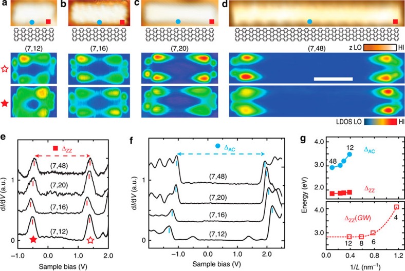
(a–d) STM topography images and STS maps of empty and filled edge states of decoupled (7, 12), (7, 16), (7, 20) and (7, 48) GNRs on NaCl monolayer islands (U=−0.1 V, I=30 pA). Colour bars: LO=low, HI=high, LDOS=local density of states. (e,f) Differential conductance spectra taken at the terminus (e) and at the centre (f) of each ribbon shown in a–d. Scale bar, 2 nm. (g) Bulk band gap ΔAC, edge state splitting ΔZZ and calculated GW splitting ΔZZ(GW) as a function of inverse GNR length (the dashed line serves as a guide to the eye).
Separation between zigzag edges
To investigate finite size effects, ribbons of different lengths have been moved onto NaCl islands and inspected. Figure 3a–d shows STM topographies (upper panel) and STS maps (lower panel) of filled and empty edge states of (7, 12), (7, 16), (7, 20) and (7, 48) GNRs, respectively. In accordance with measurements on Au(111) as well as theory17,32, the edge states are found to be localized near the zigzag termini with a typical extent of 1.5 nm (see Supplementary Note 2 for a tight-binding analysis). Over the length range of 3–10 nm investigated here, ΔZZ is essentially independent of the separation between the zigzag edges, in accordance with the G0W0 predictions (cf. Fig. 3e and Supplementary Table 1). Similar observations have also been made on long, chemically etched zigzag GNRs on SiC, where a constant gap of 0.12 eV is reported for ribbons wider than 3 nm (ref. 21). In the case of long zigzag GNRs, however, the edge-localized states overlap energetically with delocalized states8, making it difficult to distinguish between the two in STS. For (7, n) GNRs, the additional quantum confinement at the short zigzag edges selects one particular wavelength along the zigzag edge and the corresponding edge state is energetically isolated from the delocalized states of (7, ∞) GNRs.
Electronic band structure
We now turn to the delocalized bulk electronic states of decoupled (7, n) GNRs. Their width of 7=3 × 2+1 carbon dimer rows identifies (7, n) GNRs as members of the 3m+1-family of AGNRs, which have the largest band gaps7,8. Figure 3f shows dI/dV spectra taken at the centre of a (7, 12) GNR, featuring two sharp peaks at –1.2 and 2.3 V. These peaks indicate the onsets of the highest occupied and the lowest unoccupied bulk states, respectively, yielding a bulk band gap of ΔAC=3.5 eV. In contrast to the energy splitting ΔZZ of the localized edge states, we find that the bulk band gap ΔAC decreases continuously from 3.5 eV for the shortest (7, 12) GNR to 2.9 eV for the longest (7, 48) GNR under study, as shown in Fig. 3g. This trend is rationalized by the decreasing longitudinal confinement of the associated bulk states that extend throughout the GNR. Figure 3g suggests that the value of 2.9 eV, measured for a GNR of 10 nm length, is converged within experimental accuracy, in agreement with length-dependent band gap studies of (7,n) GNRs on Au(111)25. Many-body perturbation theory calculations in the GW approximation predict a band gap of 3.7±0.1 eV for freestanding (7, ∞) GNRs2,8. Although the observed band gap of ΔAC=2.9 eV is still below this value, it is significantly larger than the 2.4 eV measured for the (7, ∞) GNR on Au(111)25, thus indicating considerably reduced screening by substrate electrons.
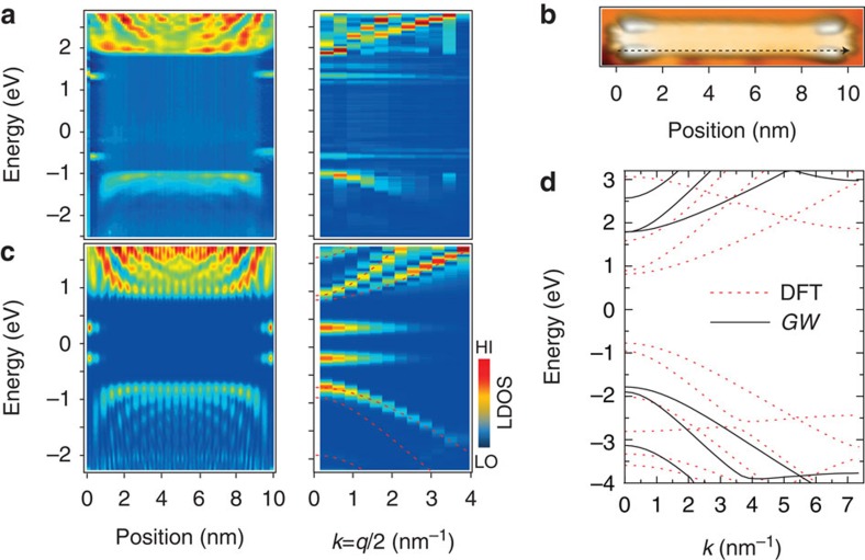
Furthermore, the dispersion of the electronic states of a decoupled (7, 48)-GNR has been determined via Fourier transformed (FT) STS25. Figure 4a shows a grid of STS spectra taken along one armchair edge. In the colour map, both the edge states and the bulk states can be resolved. The bulk states show standing waves arising from scattering at the termini of the GNRs, in good agreement with the corresponding DFT-based FT-STS simulation of a (7, 48)-GNR (Fig. 4b). For example, at −1.4 V bias, four nodes are observed along both armchair edges. With decreasing bias, we observe three nodes, two nodes and one node at −1.2, −1.1 and −1.0 V, respectively (see Supplementary Fig. 3 for constant-current STS maps). To quantitatively investigate the electronic band dispersion, we perform a discrete FT to reciprocal space as shown in Fig. 4b. One occupied band and two unoccupied bands can be resolved, with effective masses of 0.32±0.04, 0.35±0.10 and 0.20±0.05 me, respectively (me is the free electron mass). We note that the bands appear with different intensity in STS because of the finite tip-sample distance and refer interested readers to the corresponding study on Au(111) for details25. Although the effective masses are slightly smaller than those determined for the (7, ∞) GNRs directly on Au(111)25, the respective error bars overlap, indicating that the effective masses are largely unaffected by the electronic decoupling, despite the accompanying significant increase of the band gap. Figure 4c shows the DFT band structure of the (7, ∞) GNR and the corresponding many-body corrections within the G0W0 approximation. Although the band gap is found to open from 1.6 to 3.6 eV (ref. 8), the effective masses are found to decrease only by ∼10%. This finding is consistent with earlier work on graphene where many-body corrections to the local-density approximation give rise to a similar increase of the dispersion near the Fermi energy33.
Figure 4. Band structure of decoupled (7, 48) graphene nanoribbon.
(a) Left panel: Grid of dI/dV spectra (spaced 0.15 nm) taken along the armchair edge of a decoupled (7, 48) GNR. Right panel: Fourier transformed map revealing one occupied band and two unoccupied bands near the Fermi level. (b) STM topography of a decoupled (7, 48) GNR (U=−1 V, I=30 pA). (c) Left panel: DFT-based local density of states (LDOS) of (7, 48) GNR at 4 Å tip-sample distance (integrated across the ribbon). Right panel: Fourier transformed LDOS with DFT bands of infinite ribbons superposed as dashed red lines. Colour bar: LO=low, HI=high. (d) DFT and GW band structure of (7, ∞) GNR, aligned at the centre of the gap (zero energy).
Conclusions
We have demonstrated the transfer of atomically precise (7, n) graphene nanoribbons from Au(111) to an insulating monolayer of NaCl without introducing any defects. The delocalized electronic states of (7, n) GNRs are separated energetically from the states localized at the zigzag termini, making it possible to investigate the effect of electronic decoupling on both classes of states separately. Using STS, the band gap between delocalized states is found to increase from 2.4 to 2.9 eV upon electronic decoupling, whereas no significant modification of the effective masses is observed. Furthermore, we find an energetic splitting of the states localized at the zigzag termini that has long been predicted for freestanding zigzag edges, but is missing completely in (7, n) GNRs on Au(111). Both its substantial size of ΔZZ=1.9 eV and its independence on edge separation down to 3 nm are in agreement with ab initio many-body perturbation theory calculations of the GNRs' intrinsic electronic structure, indicating that decoupling by a single layer of NaCl indeed allows to study the intrinsic properties of graphene zigzag edges. We therefore expect that the experimental strategy established here will particularly benefit the eagerly awaited exploration of the low-energy spin physics at graphene zigzag edges using spin-sensitive methods.
Methods
Sample preparation and transfer procedure
Sample preparation and STM measurements were performed in an ultrahigh vacuum system (base pressure 1 × 10⁻¹⁰ mbar) using an Omicron low-temperature STM. The Au(111) substrate was cleaned by standard argon sputtering and annealing cycles. The GNRs were grown on Au(111) following the recipe by Cai et al.1. The sample temperature for the cyclodehydrogenation step was chosen such as to yield monohydrogenated termini32. NaCl powder was thermally evaporated at the sample held at room temperature. Immediately after NaCl deposition, the sample was transferred to the STM chamber and cooled down to 5 K for characterization. This results mostly in NaCl monolayers, as judged by their apparent height of 2.2 Å. To transfer a GNR onto NaCl, the GNR is picked up at one end by the STM tip22. Together with the GNR, the tip is then moved laterally above the NaCl monolayer, whereas the other end of the GNR still remains physisorbed on Au(111). After applying a voltage pulse of 3.0 V to release the ribbon, the tip is used to push the GNR fully onto the NaCl monolayer (see also Supplementary Fig. 1 and Supplementary Note 1). Transfer of GNRs onto bilayer NaCl was found to be more challenging, as partial adsorption of GNRs on NaCl bilayers was unstable. All dI/dV spectra were recorded using the lock-in technique with Urms=20 mV.
Computational methods
Electronic structure calculations within the framework of density functional theory were performed with the PBE exchange-correlation functional30. Band structure calculations were carried out using the Quantum ESPRESSO package34. The electronic structure of the (7, 48) GNR was calculated with the CP2K code35, which expands the electronic wave functions on an atom-centred Gaussian-type basis set. After extrapolating the Kohn–Sham orbitals into the vacuum region36, STS simulations were performed in the Tersoff–Hamann approximation37 on a plane parallel to the planar GNR. Quasiparticle corrections were computed in the G0W0 approximation using the BerkeleyGW package28,38. The static dielectric matrix was calculated using a rectangular Coulomb-cutoff along the aperiodic directions39 and extended to finite frequencies via the generalized plasmon pole model28. In the calculation of the self-energy, the static remainder approach was used to speed up the convergence with respect to the number of empty bands40 (more details in Supplementary Note 3).
Additional information
How to cite this article: Wang, S. et al. Giant edge state splitting at atomically precise graphene zigzag edges. Nat. Commun. 7:11507 doi: 10.1038/ncomms11507 (2016).
Supplementary Material
Supplementary Figures 1-5, Supplementary Table 1, Supplementary Notes 1-3 and Supplementary References
Acknowledgments
This work was supported by the Swiss National Science Foundation, by the Office of Naval Research BRC Program and by a grant from the Swiss National Supercomputing Centre (CSCS) under project ID s507.
Footnotes
Author contributions S.W., R.F. and P.R. conceived the experiments. The Mainz group synthesized the molecular precursors. S.W. performed the scanning probe experiments. L.T. and C.A.P. performed the simulations. S.W., L.T. and P.R. wrote the paper. All authors discussed the results and implications and commented on the manuscript at all stages.
References
- Cai J. et al. Atomically precise bottom-up fabrication of graphene nanoribbons. Nature 466, 470–473 (2010). [DOI] [PubMed] [Google Scholar]
- Ruffieux P. et al. Electronic structure of atomically precise graphene nanoribbons. ACS Nano 6, 6930–6935 (2012). [DOI] [PubMed] [Google Scholar]
- Chen Y.-C. et al. Tuning the band gap of graphene nanoribbons synthesized from molecular precursors. ACS Nano 7, 6123–6128 (2013). [DOI] [PubMed] [Google Scholar]
- Zhang H. et al. On-surface synthesis of rylene-type graphene nanoribbons. J. Am. Chem. Soc. 137, 4022–4025 (2015). [DOI] [PubMed] [Google Scholar]
- Denk R. et al. Exciton-dominated optical response of ultra-narrow graphene nanoribbons. Nat. Commun. 5, 4253 (2014). [DOI] [PubMed] [Google Scholar]
- Nakada K., Fujita M., Dresselhaus G. & Dresselhaus M. S. Edge state in graphene ribbons: nanometer size effect and edge shape dependence. Phys. Rev. B 54, 17954 (1996). [DOI] [PubMed] [Google Scholar]
- Son Y.-W., Cohen M. L. & Louie S. G. Energy gaps in graphene nanoribbons. Phys. Rev. Lett. 97, 216803 (2006). [DOI] [PubMed] [Google Scholar]
- Yang L., Park C.-H., Son Y.-W., Cohen M. L. & Louie S. G. Quasiparticle energies and band gaps in graphene nanoribbons. Phys. Rev. Lett. 99, 186801 (2007). [DOI] [PubMed] [Google Scholar]
- Yazyev O. V. Emergence of magnetism in graphene materials and nanostructures. Rep. Prog. Phys 73, 056501 (2010). [Google Scholar]
- Golor M., Koop C., Lang T. C., Wessel S. & Schmidt M. J. Magnetic correlations in short and narrow graphene armchair nanoribbons. Phys. Rev. Lett. 111, 085504 (2013). [DOI] [PubMed] [Google Scholar]
- Wimmer M., Adagideli İ., Berber S., Tománek D. & Richter K. Spin currents in rough graphene nanoribbons: universal fluctuations and spin injection. Phys. Rev. Lett. 100, 177207 (2008). [DOI] [PubMed] [Google Scholar]
- Son Y.-W., Cohen M. L. & Louie S. G. Half-metallic graphene nanoribbons. Nature 444, 347–349 (2006). [DOI] [PubMed] [Google Scholar]
- Topsakal M., Sevinçli H. & Ciraci S. Spin confinement in the superlattices of graphene ribbons. Appl. Phys. Lett. 92, 173118 (2008). [Google Scholar]
- Li Y. et al. Absence of edge states in covalently bonded zigzag edges of graphene on Ir(111). Adv. Mater. 25, 1967–1972 (2013). [DOI] [PubMed] [Google Scholar]
- Tao C. et al. Spatially resolving edge states of chiral graphene nanoribbons. Nat. Phys 7, 616–620 (2011). [Google Scholar]
- Ijäs M. et al. Electronic states in finite graphene nanoribbons: effect of charging and defects. Phys. Rev. B 88, 075429 (2013). [Google Scholar]
- van der Lit J. et al. Suppression of electron–vibron coupling in graphene nanoribbons contacted via a single atom. Nat. Commun. 4, 2023 (2013). [DOI] [PubMed] [Google Scholar]
- Drost R. et al. Electronic states at the graphene–hexagonal boron nitride zigzag interface. Nano Lett. 14, 5128–5132 (2014). [DOI] [PubMed] [Google Scholar]
- Magda G. Z. et al. Room-temperature magnetic order on zigzag edges of narrow graphene nanoribbons. Nature 514, 608–611 (2014). [DOI] [PubMed] [Google Scholar]
- Park J. et al. Spatially resolved one-dimensional boundary states in graphene–hexagonal boron nitride planar heterostructures. Nat. Commun. 5, 5403 (2014). [DOI] [PubMed] [Google Scholar]
- Li Y. Y., Chen M. X., Weinert M. & Li L. Direct experimental determination of onset of electron–electron interactions in gap opening of zigzag graphene nanoribbons. Nat. Commun. 5, 4311 (2014). [DOI] [PubMed] [Google Scholar]
- Koch M., Ample F., Joachim C. & Grill L. Voltage-dependent conductance of a single graphene nanoribbon. Nat. Nanotechnol. 7, 713–717 (2012). [DOI] [PubMed] [Google Scholar]
- Bennett P. B. et al. Bottom-up graphene nanoribbon field-effect transistors. Appl. Phys. Lett. 103, 253114 (2013). [Google Scholar]
- Repp J., Meyer G., Stojković S. M., Gourdon A. & Joachim C. Molecules on insulating films: scanning-tunneling microscopy imaging of individual molecular orbitals. Phys. Rev. Lett. 94, 026803 (2005). [DOI] [PubMed] [Google Scholar]
- Söde H. et al. Electronic band dispersion of graphene nanoribbons via Fourier-transformed scanning tunneling spectroscopy. Phys. Rev. B 91, 045429 (2015). [Google Scholar]
- Louie S. G. & Cohen M. L. Conceptual Foundations of Materials : a Standard Model for Ground- and Excited-State Properties 1st edn Elsevier (2006). [Google Scholar]
- Perdew J. P. & Levy M. Physical content of the exact Kohn-Sham orbital energies: band gaps and derivative discontinuities. Phys. Rev. Lett. 51, 1884–1887 (1983). [Google Scholar]
- Hybertsen M. S. & Louie S. G. Electron correlation in semiconductors and insulators: band gaps and quasiparticle energies. Phys. Rev. B 34, 5390–5413 (1986). [DOI] [PubMed] [Google Scholar]
- Koval P., Foerster D. & Sánchez-Portal D. Fully self-consistent GW and quasiparticle self-consistent GW for molecules. Phys. Rev. B 89, 155417 (2014). [Google Scholar]
- Perdew J. P., Burke K. & Ernzerhof M. Generalized gradient approximation made simple. Phys. Rev. Lett. 77, 3865–3868 (1996). [DOI] [PubMed] [Google Scholar]
- Jiang X. et al. Giant quasiparticle bandgap modulation in graphene nanoribbons supported on weakly interacting surfaces. Appl. Phys. Lett. 103, 133107 (2013). [Google Scholar]
- Talirz L. et al. Termini of bottom-up fabricated graphene nanoribbons. J. Am. Chem. Soc. 135, 2060–2063 (2013). [DOI] [PubMed] [Google Scholar]
- Trevisanutto P. E., Giorgetti C., Reining L., Ladisa M. & Olevano V. Ab Initio GW many-body effects in graphene. Phys. Rev. Lett. 101, 226405 (2008). [DOI] [PubMed] [Google Scholar]
- Giannozzi P. et al. QUANTUM ESPRESSO: a modular and open-source software project for quantum simulations of materials. J. Phys. Condens. Matter 21, 395502 (2009). [DOI] [PubMed] [Google Scholar]
- The CP2K developers group. . http://www.cp2k.org (2013).
- Tersoff J. Method for the calculation of scanning tunneling microscope images and spectra. Phys. Rev. B 40, 11990 (1989). [DOI] [PubMed] [Google Scholar]
- Tersoff J. & Hamann D. R. Theory of the scanning tunneling microscope. Phys. Rev. B 31, 805–813 (1985). [DOI] [PubMed] [Google Scholar]
- Deslippe J. et al. BerkeleyGW: a massively parallel computer package for the calculation of the quasiparticle and optical properties of materials and nanostructures. Comput. Phys. Commun. 183, 1269–1289 (2012). [Google Scholar]
- Rozzi C. A., Varsano D., Marini A., Gross E. K. U. & Rubio A. Exact Coulomb cutoff technique for supercell calculations. Phys. Rev. B 73, 205119 (2006). [Google Scholar]
- Deslippe J., Samsonidze G., Jain M., Cohen M. L. & Louie S. G. Coulomb-hole summations and energies for GW calculations with limited number of empty orbitals: a modified static remainder approach. Phys. Rev. B 87, 165124 (2013). [Google Scholar]
Associated Data
This section collects any data citations, data availability statements, or supplementary materials included in this article.
Supplementary Materials
Supplementary Figures 1-5, Supplementary Table 1, Supplementary Notes 1-3 and Supplementary References


