Abstract
We report on the design and testing of a custom application-specific integrated circuit (ASIC) that has been developed as a key component of the Boston retinal prosthesis. This device has been designed for patients who are blind due to age-related macular degeneration or retinitis pigmentosa. Key safety and communication features of the low-power ASIC are described, as are the highly configurable neural stimulation current waveforms that are delivered to its greater than 256 output electrodes. The ASIC was created using an 0.18 micron Si fabrication process utilizing standard 1.8 volt CMOS transistors as well as 20 volt lightly doped drain FETs. The communication system receives frequency-shift keyed inputs at 6.78 MHz from an implanted secondary coil, and transmits data back to the control unit through a lower-bandwidth channel that employs load-shift keying. The design’s safety is ensured by on-board electrode voltage monitoring, stimulus charge limits, error checking of data transmitted to the implant, and comprehensive self-test and performance monitoring features. Each stimulus cycle is initiated by a transmitted word with a full 32-bit error check code. Taken together, these features allow researchers to safely and wirelessly tailor retinal stimulation and vision recovery for each patient.
I. Introduction
The retinal neural network is a part of the brain with well-understood geographic organization; patients have provided detailed feedback on its response to electrical stimuli [1]. Advances in micro-fabrication, electronics, materials, surgical techniques and research have enabled the Boston Retinal Implant group (BRIP) to build an advanced retinal prosthesis to restore vision to patients who have lost their vision due to retinal diseases, especially retinitis pigmentosa and age-related macular degeneration. In recent years, the visual prosthetic community has expanded to more than 20 groups worldwide [1]–[3]. The collective outcome of testing (see, e.g., [4]–[5]) has provided important “proof-of-concept” evidence, including demonstration 1) of seemingly safe stimulation thresholds; 2) that severely blind patients can reliably see phosphenes; 3) that modulation of electrical stimulation alters percepts; 4) that object orientation and movement can be detected; and 5) that restoration of vision with an acuity of about 20/1000 is possible, although this often requires head movement to scan letters and considerable time to interpret the visual scene, sometimes tens of seconds. One notable result from Retina Implant AG in Germany was an implant recipient who could read one week after implantation [6]. Collectively, these results surely are encouraging, but fall short of the goal of creating more natural, higher quality vision that would more easily justify the risk of surgery and the cost of the device. The need to achieve higher quality of restored vision has motivated us as well as other teams [7]–[8] to develop advanced devices, which our team chose to do prior to performing long-term human implants. We report on the application specific integrated circuit (ASIC) that forms the heart of our new prosthetic, the wireless means used to communicate data to and from our device, and the means for processing input images gathered from a video camera mounted on glasses worn by the patient. Our results will pave the way toward human trials, and, we hope, a real improvement in quality-of-life for implant recipients.
II. ASIC Design and Testing
A. System Description
The core element of our retinal prosthesis is the ASIC that serves as its communication and control center. It is designed to receive information from an external controller, control the electrode drivers, and transmit outbound data. The ‘reverse’ telemetry includes monitoring of electrode voltage waveform data to ensure the safety of the patient and the long-term integrity of the electrodes, and data to support the debugging of implanted devices or lab experiments.
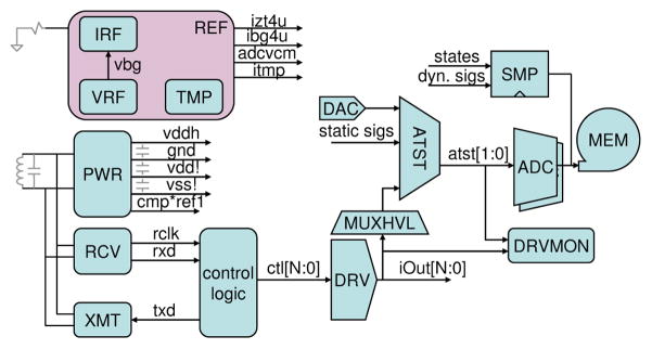
Figure 1 shows a block diagram of the BRI2 ASIC. In the upper left, a bandgap voltage reference (VRF) and an external resistor allow the REF block to distribute constant voltage and constant current references across the 5×5mm System on Chip (SoC). The TMP block generates a current proportional to absolute temperature that is used to sense changes in die temperature. The PWR block regulates on-chip power supplies, while the RCV and XMT blocks communicate with the external controller using frequency-shift-keying (FSK) and load-shift-keying (LSK), respectively. A synthesized digital control logic block interfaces between the RCV and XMT blocks and the array of electrode drivers (DRV), as well as the on-chip analog test multiplexors (ATST) that feed dual ADC’s, and the electrode voltage monitor (DRVMON) that checks for charge buildup on electrodes. An on-chip memory (MEM) captures the output of the dual ADC’s or any of a wide range of other on-chip digital signals, with a configurable sample rate and start time.
Fig. 1.
BRI2 ASIC block diagram.
Safety features include stimulus charge limits, error checking on data transmission, comprehensive self-test and performance monitoring, and configuration pins to change operating modes or to lock out settings that might somehow cause harm. This allows debugging and optimization of performance in the lab, and management of risk. A robust ACK-only protocol with strong error checking is used to communicate with the implant ASIC. Each message from the external controller can result in a set of stimulus pulses on a subset of the electrodes, and generates a corresponding response from the implant ASIC with chip and electrode status, and any other requested data. Radio communication errors are nearly eliminated by the use of 32-bit CRCs, reducing the probability of accepting a corrupted message to 2−10. No individual message can cause harm, and messages with a bad CRC merely result in missing stimulus pulses. Several features also work to ensure operation with safe levels of electrode polarization. While allowing both high-current short pulses and low-current long pulses, the ASIC has hardware-enforced charge limits, guided by our prior electrode characterization work [5]. Configuration pins allow the limits to be changed for compatibility with a range of electrode sizes. Each electrode is grounded (shorted to the case) for at least 200 μsec before any stimulus, and its voltage is monitored to ensure that the electrode is fully depolarized, and monitored again after the initial W1 pulse to ensure that electrode polarization is within safe limits (see Figure 2). The VDDH and VSS power supplies prevent excessively large voltages from being driven on electrodes. In addition, the integrated ADCs periodically sample the voltage waveforms on each electrode, sending back detailed measurements to the external controller; this allows open and short circuits to be detected, as well as changes in electrode-tissue impedance and responses over time. To reduce bandwidth requirements, an efficient message organization is used. Forward and reverse channels operate simultaneously while stimuli are ongoing. In fact, restricting the stimuli to charge-balanced waveforms for safety also reduces the degrees of freedom, and thus the number of bits needed to describe the waveforms. Figure 2 shows a first command received from the external controller (RxCommand1), which initiates a set of stimulus pulses while the subsequent RxCommand2 is being received. The commands specify the time width W1 and the sign of current for the initial pulse, along with the inter-phase width Wip and the complementary pulse width W2. For charge balance, I2 = I1 * (W1/W2).
Fig. 2.

Electrode stimulus control and waveform.
Any subset of electrodes can be driven in a given stimulus cycle, and electrodes can be configured as sources of current or as local current sinks (returns) to provide current steering capabilities. There is considerable flexibility in pulse repetition rate, and a 60 Hz refresh of all electrodes can be wirelessly commanded as needed. Power consumption is minimized in a number of ways, which ultimately limits the RF energy the recipient must be exposed to while the implant is active. Analog bias currents are typically 1μA, and are distributed to local current mirrors shared by the electrode drivers, which consume no power during the majority of the time that they are not enabled; brief power-up transients are charge-matched to first order between positive and negative voltage sources.
The ability to connect almost any analog node, including all electrodes, to on-chip ADC’s for waveform transmission back to the external controller, or to an on-chip DAC, enabled testing of much of the analog circuitry. A similar ability to capture or drive many digital signals, along with a built-in scan test, also allowed faults to be detected.
A micrograph of the BRI2 retinal implant die is shown in Figure 3. Part of the electrode driver array is in the upper two thirds of the image, and centralized bias circuitry is at the lower right; both are under a power and signal grid in the thick top metal layer. The die was fabricated in IBM’s high-voltage 0.18μm CMOS process, with 20V LD MOSFETs.
Fig 3.
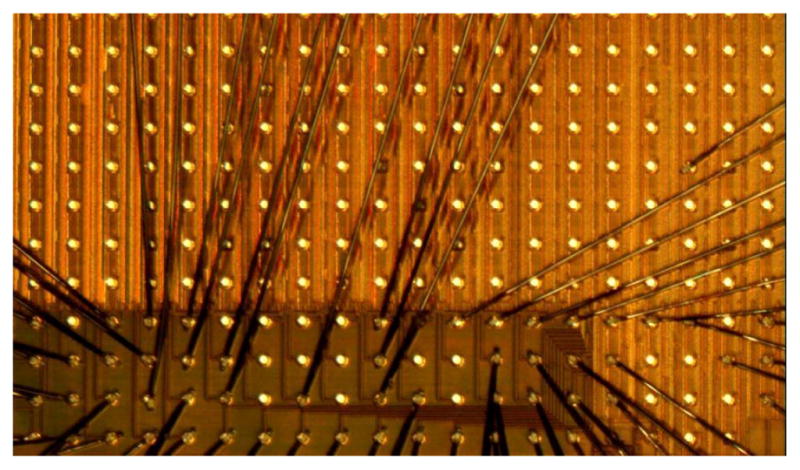
Partial, wire-bonded die photo showing some of the >256 electrode drivers, control logic, and analog circuits.
B. Verification: ASIC, Power and Data Transmission
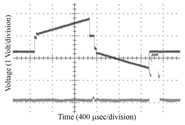
Bench testing of the ASIC using series RC electrode models was performed (see Fig. 4). The lower trace in Figure 4 represents an end-of-stimulus pulse, upon which the electrode is shorted to the current return (GND) that is connected to the platinum-coated, laser-welded Ti package.
Fig. 4.
Upper trace: typical output of the HD retinal micro-stimulator ASIC when powering an electrode modeled as a series RC circuit. Lower trace: an end-of-stimulus pulse, upon which the electrode is shorted to ground.
Figure 5 shows the external transmitter (EXTXMT) with its Class E power amplifier connected to a resonant capacitance in parallel with a 7μH primary coil (mounted in glasses that patients will wear). The 4.4μH secondary coil, implanted around the cornea, is approximately 1cm from the glasses, with coupling factor k ~ 0.14. Previous testing by our group showed that at a typical maximum angular displacement from normal alignment of the primary and secondary coils of 15 degrees due to eye movement, the transmitted power dropped off by 10% [9]. A resonant capacitor was included on a small board inside the titanium enclosure, along with Schottky diodes and capacitors to half-wave rectify a positive and negative supply relative to GND. Since our charge-balanced stimulus drew equal currents from VDDH and VSS, the dual half-wave rectification was efficient, and minimized discrete components within the package. Circuitry in the ASIC regulated VDDH and VSS to minimize power and provided accurate stimuli. The implant power supplies can run in two modes, +/− 8V, and +/− 4V. These relatively high voltages are dropped mostly across tissue; this is acceptable because of the low field due to the large distance to the GND return.
Fig. 5.
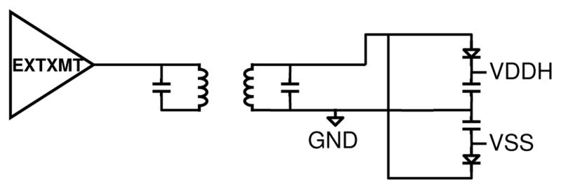
BRI2 ASIC radio and power system block diagram.
Figure 6 shows the voltages on the secondary coil, VDDH and VSS supplies during power-up of the BRI2 ASIC. The high frequency AC is occasionally attenuated at the ASIC to transmit data back to the external controller using load-shift-keying (LSK). Somewhat counter-intuitively, LSK that attenuates the secondary coil voltage resulted in a larger signal at the primary coil (in the external glasses), as less power is drawn from the coupled resonant system. Different attenuation strengths are shown, which allow for optimization of data and power transmission. In addition, the power supplies can be seen to be charging up from +/−4V on the left to +/−4.2V on the right, as power is drawn from the secondary coil via the Schottky diodes.
Fig. 6.
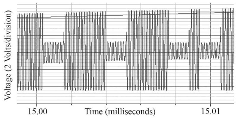
Secondary coil, VDDH and VSS with simultaneous FSK and LSK.
A final test was to transmit data to the chip using the RF transmitter. Data reception is demonstrated in Fig. 7, in which the top trace represents the chip’s sampling clock, the middle waveform represents the received data (which is valid at the rising edge of the sampling clock), and the bottom trace represents the data fed to the transmitter board.
Fig. 7.
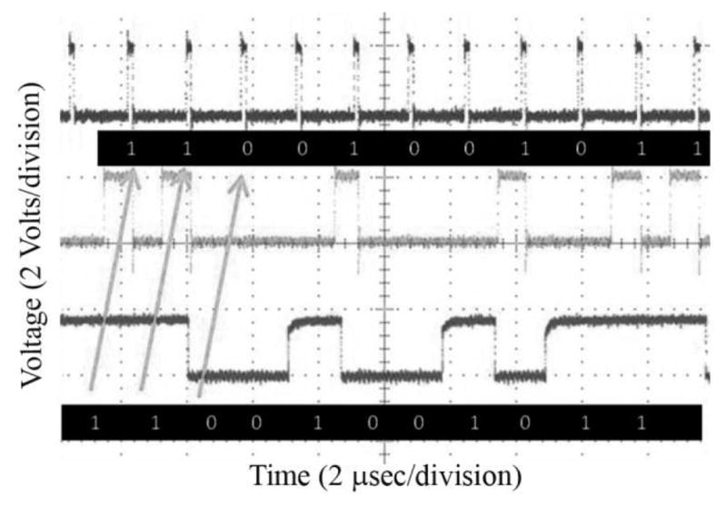
Wireless data transmission to the retinal implant ASIC.
C. Video Image Pre-Processing
We are currently developing image processing software for the retinal implant and the user interface that patients and clinicians will use together to adjust video pre-processing to achieve the best visual percepts. Images are captured by a glasses-mounted camera at 30 frames/sec and then sent to the external controller, where they are loaded into memory as a 640 × 480 color (RGB) image. They are then converted to grayscale (7-bit) and sent through a series of user-defined filters, chosen e.g. from contrast enhancement, edge extraction, blurring, and thresholding. After filtering, the image is down-sampled to >256 points, one for each electrode. The camera’s automatic gain control compensates for varying ambient light levels. The choice of which algorithms to use and what parameters to set for each filter is likely to vary across patients, across different lighting environments, and may also depend on the task that the user is performing. Figure 8 shows an illustration of what video processing might look like. The raw image is sent through a thresholding filter and then down-sampled, where each point is spatially aligned with the position of an electrode. Using our user interface, each filter can be turned on or off, and its parameters can be adjusted. The white box in the top left image of Fig. 8 represents a zoom window, allowing the user to zoom in or out on a scene. Currently, the image processing algorithms are implemented on a personal computer running C++/‘OpenCV’. Depending on the extent of the image processing, we achieve frame rates from 5 to 20 frames/sec. In the portable version of our device, we will implement these algorithms using a dedicated DSP to achieve sufficient computation speed in the embedded system. We anticipate that optimized patient input for image processing algorithms (and stimulation parameters, within safe limits) will be determined in an iterative fashion.
Fig. 8.
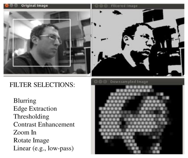
Video filtering and down-sampling for the retinal implant.
III. Conclusions and Future Work
We have designed and extensively bench-tested a highly configurable, high-density neuro-stimulator ASIC in both wired and wireless configurations. This >256 channel device is appropriate for chronic implantation with our proven, minimally-invasive sub-retinal surgical implantation techniques, and its sophisticated LSK reverse telemetry features will enable optimization of stimuli for each patient. Extensive safety features have been implemented in this chip; driving software, GUI development, and image processing algorithms for the external system are under development, as we prepare for pilot human trials of our retinal prosthesis.
Table 1.
BRI2 Implant ASIC Technical Specifications
| Power: 6.78 MHz carrier; ~30 mW transmitted |
| Data: 565 Kbps inbound, 70 Kbps outbound |
| Electrode Current: 0 – 127 μA in 1 μA steps |
| Stimulus Pulse width: 17.7 – 4500 μsec; up to +/− 8V |
Acknowledgments
This work was supported in part by the U.S. Department of Veterans Affairs, Rehabilitation Research and Development Division, through Center of Excellence grant C4266-C. Additional support was provided by NIH grant EY016674 to Prof. Wyatt at MIT, by the NSF’s support of the Cornell NanoScale Facility and Prof. Wyatt, by the Massachusetts Lions Foundation, and by private sources.
The authors thank W. Hansford and MOSIS, M. Lugin and M. Segien for custom layout work, G Galanek and J. Dumser for administrative assistance, the Cornell Nano-fabrication staff, and S. Behan for his engineering expertise.
Contributor Information
Douglas B. Shire, Email: dbs6@cornell.edu, Boston VA Healthcare System, 150 S. Huntington Ave., Boston, MA 02130 phone: +1 (607) 339-7085; fax: (607) 255-8601.
Shawn K. Kelly, Boston VA Healthcare System, 150 S. Huntington Ave., Boston, MA 02130.
Patrick Doyle, Harvest Automation, Billerica, MA 01862 USA.
Attila Priplata, Massachusetts Eye and Ear Infirmary, Boston, MA 02114.
William Drohan, Boston VA Healthcare System, 150 S. Huntington Ave., Boston, MA 02130.
Oscar Mendoza, Massachusetts Institute of Technology, Cambridge, MA 02139.
Marcus Gingerich, Boston VA Healthcare System, 150 S. Huntington Ave., Boston, MA 02130.
Bruce McKee, Boston VA Healthcare System, 150 S. Huntington Ave., Boston, MA 02130.
John L. Wyatt, Massachusetts Institute of Technology, Cambridge, MA 02139.
Joseph F. Rizzo, III, Massachusetts Eye and Ear Infirmary, Boston, MA 02114.
References
- 1.Rizzo JF, III, Wyatt J, Humayun M, de Juan E, Liu W, Chow A, Eckmiller R, Zrenner E, Yagi T, Abrams G. Retinal prosthesis: an encouraging first decade with major challenges ahead. Ophthalmol. 2008;108:13–14. doi: 10.1016/s0161-6420(00)00430-9. [DOI] [PubMed] [Google Scholar]
- 2.Loewenstein JI, Montezuma SR, Rizzo JF., III Outer retinal degeneration: an electronic retinal prosthesis as a treatment strategy. Arch Ophthalmol. 2004;122:587–596. doi: 10.1001/archopht.122.4.587. [DOI] [PubMed] [Google Scholar]
- 3.Weiland JD, Liu W, Humayun MS. Retinal prosthesis. Ann Rev Biomed Eng. 2005;7:361–401. doi: 10.1146/annurev.bioeng.7.060804.100435. [DOI] [PubMed] [Google Scholar]
- 4.Alteheld N, Roessler G, Walter P. Towards the bionic eye - the retina implant: surgical, opthalmological and histopathological perspectives. Acta Neurochir Suppl. 2007;97:487–493. doi: 10.1007/978-3-211-33081-4_56. [DOI] [PubMed] [Google Scholar]
- 5.Shire DB, Kelly SK, Chen J, Doyle P, Gingerich MD, Cogan SF, Drohan WA, Mendoza O, Theogarajan L, Wyatt JL, Rizzo JF., III Development and implantation of a minimally invasive wireless subretinal neurostimulator. IEEE Trans Biomed Eng. 2009;56:2502–2511. doi: 10.1109/TBME.2009.2021401. [DOI] [PMC free article] [PubMed] [Google Scholar]
- 6.Zrenner E, Bartz-Schmidt KU, Benav H, Besch D, Bruckmann A, Gabel VP, Gekeler F, Greppmaier U, Harscher A, Kibbel S, Koch J, Kusnyerik J, Peters T, Stingl K, Sachs H, Stett A, Szurman P, Wilhelm B, Wilke R. Subretinal electronic chips allow blind patients to read letters and combine them to words. Proc Biol Sci. 2011;278:1489–1497. doi: 10.1098/rspb.2010.1747. [DOI] [PMC free article] [PubMed] [Google Scholar]
- 7.Chen K, Yang Z, Hoang L, Weiland J, Humayun M, Liu W. An integrated 256-channel epiretinal prosthesis. IEEE J Solid-State Circuits. 2010;45:1946–1956. [Google Scholar]
- 8.Tran N, Skafidas E, Yang J, Bai S, Fu M, Ng D, Halpern M, Mareels I. A prototype 64-electrode stimulator in 65nm CMOS process towards a high density epi-retinal prosthesis. Conf Proc IEEE Eng Med Biol Soc. 2011:6729–6732. doi: 10.1109/IEMBS.2011.6091660. [DOI] [PubMed] [Google Scholar]
- 9.Kelly SK, Doyle P, Priplata A, Mendoza O, Wyatt JL. Optimal primary coil size for wireless power telemetry to medical implants. Conf Proc IEEE ISABEL Int Symp on Appl Sci in Biomed and Comm Tech. 2010 [Google Scholar]


