Abstract
Understanding how the mechanism of charge transport through molecular tunnel junctions depends on temperature is crucial to control electronic function in molecular electronic devices. With just a few systems investigated as a function of bias and temperature so far, thermal effects in molecular tunnel junctions remain poorly understood. Here we report a detailed charge transport study of an individual redox-active ferrocene-based molecule over a wide range of temperatures and applied potentials. The results show the temperature dependence of the current to vary strongly as a function of the gate voltage. Specifically, the current across the molecule exponentially increases in the Coulomb blockade regime and decreases at the charge degeneracy points, while remaining temperature-independent at resonance. Our observations can be well accounted for by a formal single-level tunnelling model where the temperature dependence relies on the thermal broadening of the Fermi distributions of the electrons in the leads.
 The effect of temperature on charge transport mechanisms in molecular tunnel junctions is not fully understood. Here, charge transport studies of a redox-active molecule unveil multiple mechanistic regimes which may be explained by thermal broadening of the Fermi distributions of electrons in the leads.
Tunnelling of electrons across molecular junctions depends on both temperature and applied bias. So far only a few systems have been reported that switch the mechanism of charge transport as a function of bias and temperature, resulting, for example, in good molecular diodes1,2,3,4 or enabling long-range charge transfer along molecular wires5,6,7,8,9 or biomolecules10,11,12,13. Typically, such measurements display a transition between a temperature insensitive regime, governing conduction at sufficiently low temperatures, and a thermally assisted transport regime, characterized by an exponential dependence with temperature. However, neither the origin of the thermal excitation nor the nature of the tunnelling process (coherent versus incoherent) are fully understood in solid-state junctions. For example, anomalous temperature-independent long-range (up to 16 nm) charge transport phenomena have been reported, which cannot be straightforwardly explained with current theories6,12,13. Hence, it is important to deepen our understanding of how temperature influences charge transport phenomena in molecular junctions and how this information can be used to improve their electronic characteristics.
Usually, temperature-independent conduction in molecular junctions is associated with coherent tunnelling involving the molecular level nearest in energy to the Fermi level of the leads (that is, the highest occupied molecular orbital (HOMO) or the lowest unoccupied molecular orbital)5,14,15,16. In this regime, the contact time of the charge carrier with the molecule is smaller than the intramolecular dephasing times. In contrast, an exponential increase of current with temperature is associated with an incoherent process, where the charge spends enough time in the molecule to allow decoherence14. In a wet electrochemical environment, where the current (I) increases with temperature (T) following the Arrhenius law ( , where kB is the Boltzmann constant and I0 is a pre-exponential factor), the physical meaning of the activation energy Ea is well-understood. It relates to thermal excitations of molecular vibrational modes and reorganization of neighbouring solvent molecules, (that is, inner- and outer-sphere reorganization processes, respectively17). In solid-state molecular junctions, however, the absence of solvent molecules leaves the physical meaning of Ea unclear18. Without intermolecular interactions, thermally activated interactions are restricted to coupling of the charge carrier to vibronic states of the molecular bridge, although the associated activation energies are often too low (<0.1 eV) to explain the observations. In this scenario, the value of Ea depends also on charge image effects and the corresponding re-normalization of the molecular energy levels in the junction as a result of proximity with the metallic electrodes19,20,21. Thermal broadening of the Fermi occupation distribution of electrons in the leads and its overlapping with the molecular levels has been invoked as a cause of thermally activated conduction through a single-molecule tunnel junction22,23.
By far, most temperature-dependent charge transport studies have been conducted with two-terminal junctions based on self-assembled monolayers (SAMs) or single molecules contacted by conductive probes. These approaches so far only made it possible to investigate a limited range of temperatures close to room temperature and lack a gate electrode1,24,25,26,27,28,29,30. Although molecular single-electron transistors (SETs) obtained via mechanical or electromigration techniques have a gate electrode enabling full control over the energy-level alignment of the system, these junctions are normally kept at cryogenic temperatures to ensure stability22,31,32,33,34,35,36. It is therefore necessary to expand such temperature-dependent measurements in individual molecules by studying molecules that have been well characterized with other techniques (for example, SAM-based junctions) for comparative analysis.
Here we report electromigrated three-terminal junctions with single molecules where the conduction level is well localized within the molecule and isolated from the electrodes. We use a broad range of source-drain bias and gate voltages to study the temperature dependence of the junction across three conduction regimes: (i) the Coulomb blockade regime (where the molecular level lies outside the conduction-bias window); (ii) at the charge degeneracy point (where the level lies in between the electrostatic potential of the leads); and (iii) at resonance (where the molecular level matches the energy of one of the leads).
Results
Junction fabrication
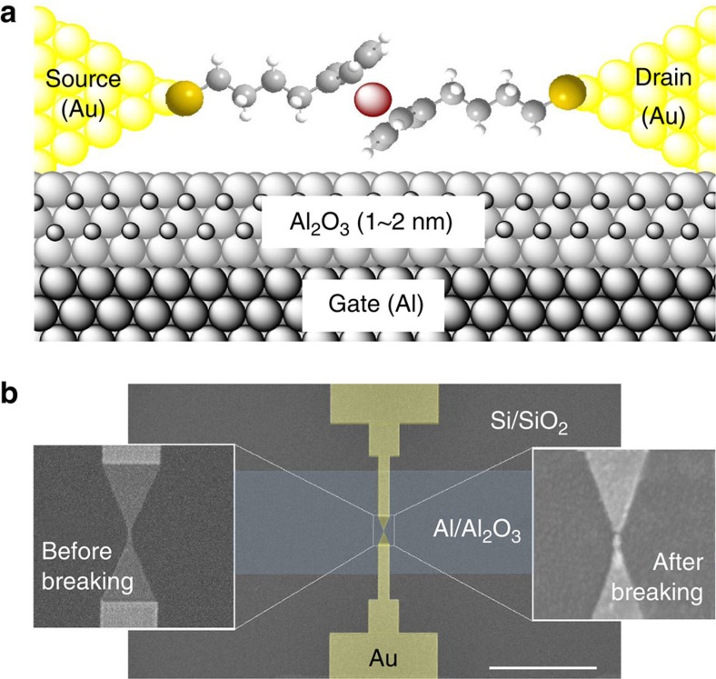
Figure 1a shows schematically the single-molecule transistor with a S-(CH2)4-Fc-(CH2)4-S (Fc=ferrocene) molecule used in this study (see Supplementary Methods). Similar molecules have been systematically studied in SAM-based junctions1,2,3,37,38,39,40, showing that at least three CH2 units between the Fc and thiolate-metal bond are needed to localize the HOMO on the Fc unit3. In our experiments, the molecule is connected to the source and drain electrodes via a metal-thiolate bond and the redox-active Fc unit is well separated from the leads by two -(CH2)4- tethers to avoid delocalization of the HOMO, which is centred at the Fc. Figure 1b shows an SEM image of a three-terminal SET fabricated by means of electron-beam and optical lithography41 (see Methods section for details).
Figure 1. The single molecule junctions.
(a) Schematic of a S-(CH2)4-Fc-(CH2)4-S molecule bridging the nanogap between the two bias leads of a SET. (b) False colour scanning electron microscopy (SEM) image of one of our SETs showing the gold nanowire on the Al/Al2O3 back gate. The scale bar is 10 μm. The insets show the thinnest part of nanowire before and after the feedback-controlled electromigration-induced breaking. The molecule completes the device by bridging the resulting nanogap during deposition from solution.
Charge transport measurements
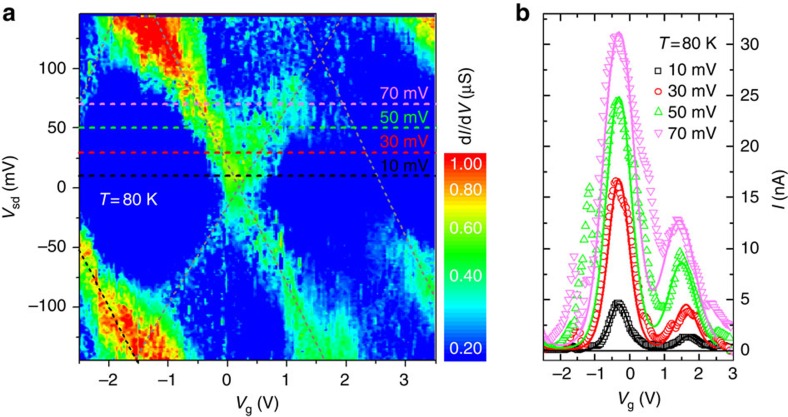
Figure 2a shows the differential conductance (dI/dV) of the molecule at 80 K as a function of source-drain Vsd (−150, +150 mV) and gate Vg (−2.5, +3.5 V) voltages. Closed diamonds characteristic of single-electron transport are clearly observed, with resonant transport excitations crossing at zero bias at two visible degeneracy points (Vg=0.25 and 2.5 V), separating the Coulomb blockade areas where no current flows through the molecule (dark blue areas). Figure 2b shows the source-drain current, I, as a function of gate voltage for different bias voltages corresponding to the horizontal colour-coded dashed lines in Fig. 2a (the solid lines are fits to the model described below). The two consecutive charge degeneracy points start to intermix for the highest bias voltages (Vsd=50 and 70 mV). The ratios of capacitive coupling C between Fc and the gate (g), source (s) and drain (d) electrodes can be extracted from the slopes of the resonant transport excitations (indicated by the tilted, dashed grey lines in Fig. 2a). The ratios are Cg:Cs:Cd=1:11:13, which determine a gate coupling parameter of gc∼0.05, characteristic for a thin Al2O3 layer separating the molecule from the gate22. From these observations, we conclude that the Fc unit is localized in the middle of the junction (Cs≈Cd) and the HOMO energy level can be efficiently gated.
Figure 2. Charge transport at 80 K.
(a) Differential conductance of a junction with S-(CH2)4-Fc-(CH2)4-S at T=80 K. The colour code represents the conductance (dI/dV) through the SET as a function of Vsd and Vg. The grey dashed lines indicate the main resonant excitations, crossing at two visible charge degeneracy points at Vsd=0 (that is, Vg=0.25 and 2.5 V) and separating the Coulomb blockade areas. A third charge degeneracy point is estimated to lie around −3.5 V. (b) Current versus gate voltage for four different bias voltages (10, 30, 50 and 70 mV). Symbols represent experimental values and solid lines are fits to the single-level tunnelling transport model (equation 1) using the parameters given in Table 1. The colour code corresponds to the horizontal dashed lines in a. The molecule most likely changed its conformation within the SET electrodes between both measurements resulting in a shift in the position of the degeneracy points (new positions: Vg=−0.3 and 1.7 V).
Temperature-dependent transport measurements
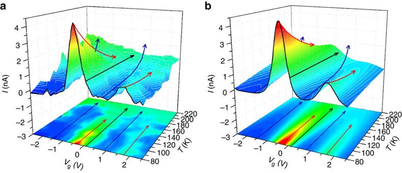
Figure 3a shows a 3D plot of I versus Vg and T for Vsd=10 mV. The data were collected as the gate voltage was continuously swept from −2.5 to +2.5 V at each temperature, and the process repeated at different temperatures from 80 to 220 K. Similar results obtained for a second device are given in Supplementary Note 1 and Supplementary Figs 1 and 2, as well as a discussion of the reversibility of the temperature behaviour of the molecular junction in the Supplementary Note 3 and Supplementary Fig. 4. Figure 3b is the corresponding theoretical plot using the single-level model described below. From these data, we can identify three transport regimes, each of which with a distinct dependence on the temperature as indicated by the arrows: (i) the Coulomb blockade regime, with I increasing exponentially with increasing T (blue arrows); (ii) the charge degeneracy points, with I decreasing with T (red arrows); and (iii) the resonant regime (when the molecular level matches the electrostatic potential of one of the leads), with I constant with T (black arrows).
Figure 3. Variable temperature charge transport.
(a) 3D plot of the evolution of the tunnel current through a S-(CH2)4-Fc-(CH2)4-S junction versus gate voltage as the temperature is increased from 80 to 220 K for Vsd=10 mV. The evolution of the two charge degeneracy points (−0.3 and 1.7 V), whose magnitude decreases with increasing temperature, can be appreciated following the red arrows in both the 3D data and its 2D horizontal projection in the Vg-T plane. Similarly, the increase with temperature in the Coulomb blockade areas can be seen by following the blue arrows. The black arrow shows the case for which the molecular level matches the electrostatic potential of one of the leads (resonance), a situation leading to almost negligible temperature dependence. (b) Corresponding response of the junction as calculated from the single-level tunnelling transport model in equation (1) using the parameters given in Table 1.
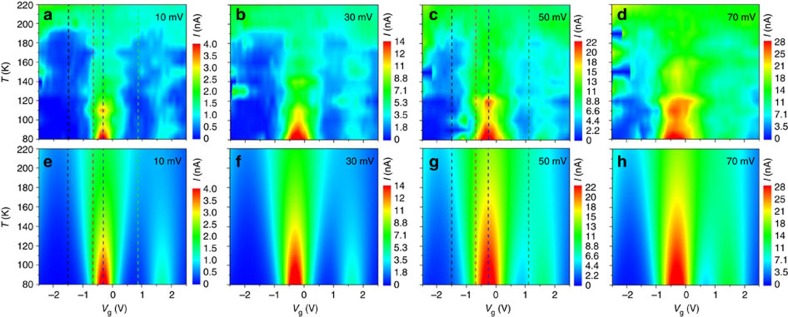
Measurements of the temperature dependence of the current were repeated at different bias values (Vsd=10, 30, 50 and 70 mV). Figure 4 shows the corresponding contour plots for each bias voltage and how the transport excitations at the degeneracy points broaden as a function of bias. The magnitude of I exhibits an overall increase as the value of Vsd increases, as can be seen from the colour-code level bars. Still, the distinct transport regimes and their respective temperature dependencies remain present for all examined Vsd values.
Figure 4. Variable temperature and source-drain voltage charge transport.
Contour colour-code plots of the current as a function of the gate voltage and temperature for both experimental data (a–d) and calculations (e–h) using the single-level tunnelling transport model in equation (1) for Vsd=10, 30, 50 and 70 mV. The vertical dashed lines in a,c,e and d indicate data and calculations presented in Fig. 5.
Single-level transport model
We have used a single-level tunnelling model to fit our experimental data using parameters that can be experimentally verified based on the Landauer formalism42,43. The conduction through the junction can be described as sequential tunnelling (either coherent or incoherent) from the right electrode into a single molecular level at a rate γR, and from the molecule into the left electrode at a rate γL, one electron at a time. The molecular level broadens to a width γ=γL+γR as a result of its interaction with the respective electrodes. Sequential coherent tunnelling through a single-level molecular junction results in electrical current given by the expression derived by Jauho, Wingreen and Meir in 1994 (ref. 44) using a fully coherent formulation based on the Keldysh Green's function formalism:
 |
where q is the charge of the electron and h is the Planck's constant. The molecular level is described by a broadened density of states Dɛ in the shape of a Lorentzian centred at the molecular level energy ɛ, as follows:
 |
with the position of the molecular level with respect to the electrostatic potentials, μL,R, of the transistor leads given by ɛ=μR(V)+ɛ0+ηqVsd. Here, η=VR/(VL+VR) is the dimensionless division parameter giving the ratio of the voltage drop between the molecule and the right electrode with respect to the total voltage drop in the junction. In other words, η represents the degree of symmetry of the electrostatic potential profile across the junction, with η=0.5 representing a completely symmetric molecule and η∼0 or 1 accounting for a highly asymmetric potential drop at both sides of the molecule. In our junctions, η=0.5 as determined from the similar slopes of the transport excitations in Fig. 2a (that is, Cs≈Cd). Finally, the effect of temperature is included in equation (1) through the Fermi distributions of the electron occupation in the leads, given by:
 |
It is important to realize that for high enough temperatures (that is,  ), equation (1) reduces to
  , which is the exact result one would obtain using rate equations to describe incoherent tunnelling through a single level in a molecular junction42,43. Indeed, in the case that only one molecular level is involved in the conduction through the junction (which is the case in the absence of intramolecular charge relaxation), coherent and incoherent descriptions of the process become indistinguishable for all temperatures if one also considers level broadening when solving the rate equations. Note that vibrational excitations of the molecule itself would open new channels for conduction, however, the low energies associated with these excitations (<30 meV; ref. 45) allow renormalizing the molecular level by simply increasing γL,R in equation (2).
Interpretation of the temperature dependencies
To explain the temperature behaviour of the current in the junction, we fitted all data to the model given by equation (1) using the parameters listed in Table 1 (solid lines in Figs 2b, 3b and 4e–h). Three molecular levels were used to account for the three degeneracy points observed within the window of electrical potentials. In essence, only two free-fitting parameters are used per molecular level to fit the results with equation (1), that is, the respective tunnelling rates γL,R. The energy levels, ɛ, are independently determined from the experimental data in Fig. 2a.
Table 1. The fitting parameters used to model the experimental data*.
| Vsd (mV) | ɛ1† (mV) | γ1L (mV) | γ1R (mV) | ɛ2† (mV) | γ2L (mV) | γ2R (mV) | ɛ3† (mV) | γ3L,R (mV) |
|---|---|---|---|---|---|---|---|---|
| 10 | 25 | 1 | 0.120 | 185 | 3 | 0.040 | −225 | 0.20 |
| 30 | 25 | 4 | 0.155 | 180 | 7 | 0.042 | −225 | 0.24 |
| 50 | 25 | 7 | 0.160 | 170 | 15 | 0.060 | −225 | 0.27 |
| 70 | 25 | 10 | 0.170 | 165 | 20 | 0.075 | −225 | 0.30 |
*The model is given by equation (1).
†The values of the three molecular levels ɛ1, ɛ2 and ɛ3, were experimentally determined from I versus Vg−Vsd data.
The energetic difference between the main two energy levels Δɛ1,2 (=ɛ1−ɛ2)=160 mV (for Vsd=10 mV), decreases slightly with increasing Vsd (140 meV for Vsd=70 mV). This reduction in the value Δɛ1,2 has been observed in other molecular tunnel junctions22, and is associated with the static Stark effect46. This shift was taken into consideration in the fitting procedure. The third level, ɛ3, responsible for the degeneracy point outside the gate voltage window (Vg∼3.5 V) is included to account for the increase in conduction for Vg<−2 V, but its position with respect to ɛ1, that is, Δɛ1,3 (=ɛ1−ɛ3), was kept constant in the model as its exact value could not be measured accurately. Highly asymmetric tunnelling rates γL≠γR for the main two levels had to be used to fit the results, with values similar to those reported for other molecular SETs22. The reason lies in the fact that these rates present two main effects on the conduction through the junction. On one hand, the sum of the right and left tunnelling rates determines the zero-temperature width of the level at each bias (γ=γL+γR), and therefore the highest rate is fixed by the experimental widths of the transport excitations. On the other hand, the lowest rate limits the current through the junction, and therefore is fixed by the experimentally observed value.
Discussion
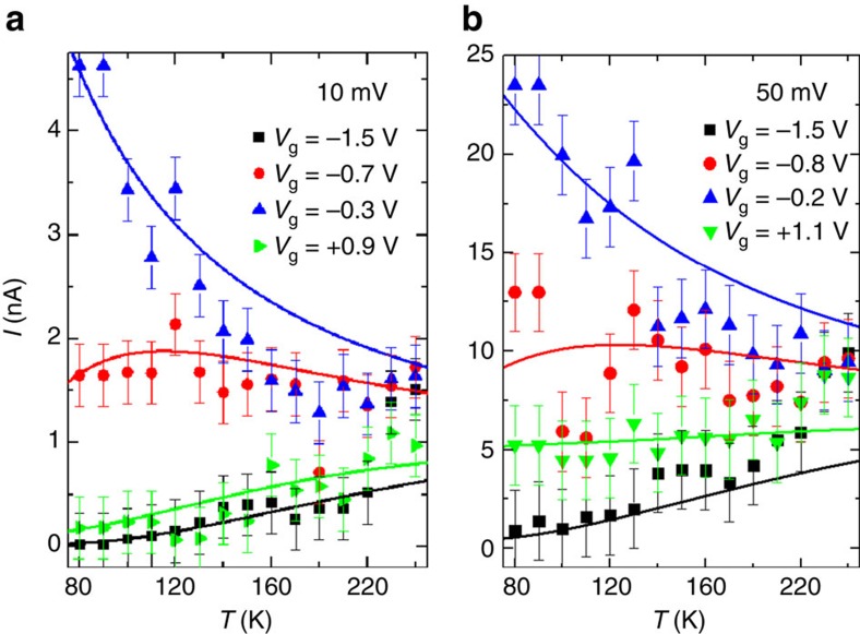
Figures 2, 3, 4 show the excellent agreement between the experimental data and the model, which indicates that the complex temperature dependence of the tunnelling current in all three transport regimes arises from the thermal broadening of the Fermi electronic occupation distribution in the leads. The quantitative degree of agreement between experiment and theory is easier to appreciate in Fig. 5, which displays the behaviour of I as a function of T for two bias voltages (Vsd=10 and 50 mV, respectively) with the values of Vg indicated by vertical lines in Fig. 4a,c specifically selected to sample the different conduction regimes. These figures clearly show how the electrostatic potential controls the conduction regime across the molecule: (i) the junction is in the Coulomb blockage regime for Vg=−1.5 (black squares) and +0.9 V (green triangles) for Vsd=10 mV (Fig. 5a) and for Vg=−1.5 and +1.1 V and Vsd=50 mV (Fig. 5b). In this regime, I exponentially increases with T (see Supplementary Note 2 and Supplementary Fig. 3 for a discussion of a crossover into a temperature-independent transport as the temperature is further decreased in this regime); (ii) the junction is at a charge degeneracy point for Vg=−0.3 V and Vsd=10 mV (Fig. 5a) and Vg=−0.2 V and Vsd=50 mV (Fig. 5b). In this regime, I decreases with T; and, finally (iii) the junction is at resonance for Vg=−0.7 V and Vsd=10 mV (Fig. 5a) and Vg=−0.8 V and Vsd=50 mV (Fig. 5b). In this regime, I depends weakly on T.
Figure 5. Tunnelling current as function of temperature and applied bias.
(a) Evolution of the tunnel current with temperature at Vsd=10 mV for four different gate voltages (Vg=−1.5, −0.7, −0.3 and +0.9 V). (b) Same for Vsd=50 mV (Vg=−1.5, −0.8, −0.2 and +1.1 V). The solid lines in both panels represent fittings to the single-level tunnelling transport model in equation (1) with the parameters given in Table 1. The error bars represent the uncertainty in the determination of the value of the tunnelling current due to the noise of the measurements.
In conclusion, our measurements reveal a complex temperature-dependent behaviour of charge transport phenomena in a ferrocene-based single-molecule junction over a wide range of bias and gate voltages. Exceptionally, we find three transport regimes in which the tunnelling current across the molecule increases, decreases, or remains constant as a function of temperature, depending on whether the junctions are tuned into the Coulomb blockade, the charge degeneracy point or the resonant transport regimes. All of our observations can be rationalized by a Landauer-type single-level model, where the complex temperature-dependent tunnelling behaviour can be explained by the broadening of the Fermi distributions accounting for the occupation energies of electrons in the transistor leads. The results described in this article represent an important step forward in explaining the temperature-dependent charge transport measurements observed in SAM-based and other single-molecule tunnelling junctions and hopefully help to improve existing models of charge transport. Currently, we are investigating junctions with asymmetrically positioned Fc moieties inside the junctions.
Methods
Synthesis of AcS(CH2)4Fc(CH2)4Sac
We prepared AcS(CH2)4Fc(CH2)4SAc from native ferrocene in three steps using well-established procedures (see Supplementary Methods, Supplementary Fig. 8 and refs 47 and 48). All compounds were characterized with 1H NMR, 13C NMR and ESI HRMS. Briefly, ferrocene was substituted with 4-bromobutanoyl chloride via a Friedel-Crafts acylation to yield (Br(CH2)3CO)2Fc (1.5 g, 45% yield). Next, this compound was reduced with borane-tert-butylamine to yield (Br(CH2)4)2Fc (1.2 g, 88% yield). The bromine functionality was converted to a thioacetate functionality with potassium thioacetate and the AcS(CH2)4Fc(CH2)4SAc was isolated with a yield of 95% (1.0 g).
This thioacetate derivative is stable and was stored under an atmosphere of N2 at −20 °C. We found that the isolation of the free dithiol was problematic because of disulfide formation. Hence our choice to isolate and use the thioacetate protected derivative, which was deprotected in situ for self-assembly of the junction.
Device fabrication
For the fabrication of the SETs thin gold nanowires (15 nm thick, 50 nm wide) patterned via electron-beam lithography were deposited on top of an Al/Al2O3 back gate electrode (1–2 nm-thick oxide barrier)41. We used a feedback-controlled electromigration-induced breaking procedure to narrow the nanowires. Once the current dropped close to the universal single-channel conductance (G0), the current flow was stopped at which point the devices were left untouched for 2 h during which the gold atoms reorganize due to surface tension to finally create stable gaps of 1–2 nm. After the self-rupture of the wires, the chip was immersed in a 1 mM solution of AcS(CH2)4Fc(CH2)4SAc in 20 ml toluene and 5 ml methanol along with 10 mg of n-Bu4NCN (CAS 10442-39-4). Here, n-Bu4NCN in this toluene/methanol mixture deprotects the thioacetate mildly49,50. Finally, the devices were mounted in a low temperature probe and cooled down to liquid nitrogen temperatures. Out of 322 devices, 11 (∼3.5%) showed molecular transport characteristics, but only two junctions (∼0.6%) were stable enough for studies as a function of temperature (80–220 K shown in the main text, and 80–250 K shown in the Supplementary Note 1 and Supplementary Fig. 1), with molecular conformational changes as the most possible cause for device instability in the other cases. We note that charge transport measurements of molecular SETs at elevated temperatures are challenging because of the high chances for the molecule to change its conformation. We also want to remark that the yield in our experiments is similar to those in most reports of molecular single-electron transistors (see, for example, refs 22, 45, which are most closely related to this work). To ensure that our devices contained a ferrocene-based molecule, we include in the Supplementary Information details of the junctions fabrication and characterization of the nano-gaps (Supplementary Methods and Supplementary Fig. 5), detailed information on the protocols for recognition and selection of ferrocene-based junctions, including measurements with magnetic fields dependent transport (Supplementary Methods and Supplementary Fig. 6), and tests of the electrical characteristics of empty junctions as a function of temperature (Supplementary Methods and Supplementary Fig. 7).
Transport measurements
Transport measurements were performed in DC by applying the bias voltage and measuring the current via a Keithley 6430 sub-femtoamp remote sourcemeter, while a Keithley 2400 was used to gate the transistor. The device was mounted on the sample holder of a home-made measuring probe with temperature control immersed in a liquid nitrogen dewar.
Data availability
All relevant data are available from the authors upon request.
Additional information
How to cite this article: Garrigues, A. R. et al. Electrostatic control over temperature-dependent tunnelling across a single-molecule junction. Nat. Commun. 7:11595 doi: 10.1038/ncomms11595 (2016).
Supplementary Material
Supplementary Figures 1-8, Supplementary Table 1, Supplementary Notes 1-3, Supplementary Methods and Supplementary References
Acknowledgments
A.R.G. and E.d.B. acknowledge support from the National Science Foundation (grants NSF-ECCS #1402990 and #1518863). C.A.N. acknowledges support from the National Research Foundation, Prime Minister's Office, Singapore under its Medium-Sized Centre programme, and the NRF fellowship award No. NRF-RF 2010-03. Singapore Ministry of Education (MOE) for supporting this research under award No. MOE2015-T2-1-050.
Footnotes
Author contributions A.R.G. conducted the single-electron transport measurements. L.W. synthesized and characterized the ferrocene-based molecules. E.d.B. and C.A.N. conceived and supervised the experimental activities. All the authors contributed to the writing of the article and interpretation of the results.
References
- Nijhuis C. A., Reus W. F., Barber J., Dickey M. D. & Whitesides G. M. Charge transport and rectification in arrays of SAM-based tunneling junctions. Nano Lett. 10, 3611–3619 (2010). [DOI] [PubMed] [Google Scholar]
- Yuan L., Breuer R., Jiang L., Schmittel M. & Nijhuis C. A. A molecular diode with a statistically robust rectification ratio of three orders of magnitude. Nano Lett. 15, 5506–5512 (2015). [DOI] [PubMed] [Google Scholar]
- Yuan L. et al. Controlling the direction of rectification in a molecular diode. Nat. Commun. 6, 6324 (2015). [DOI] [PubMed] [Google Scholar]
- Yoon H. J. et al. Rectification in tunneling junctions: 2,2′-bipyridyl-terminated n-alkanethiolates. J. Am. Chem. Soc. 136, 17155–17162 (2014). [DOI] [PubMed] [Google Scholar]
- Ho Choi S., Kim B. & Frisbie C. D. Electrical resistance of long conjugated molecular wires. Science 320, 1482–1486 (2008). [DOI] [PubMed] [Google Scholar]
- Yan H. et al. Activationless charge transport across 4.5 to 22 nm in molecular electronic junctions. Proc. Natl Acad. Sci. USA 110, 5326 (2013). [DOI] [PMC free article] [PubMed] [Google Scholar]
- Smith C. E. et al. Length dependent nanotransport and charge hopping bottlenecks in long thiophene-containing π-conjugated molecular wires. J. Am. Chem. Soc. 137, 15732–15741 (2015). [DOI] [PubMed] [Google Scholar]
- Lafferentz L. et al. Conductance of a single conjugated polymer as a continuous function of its length. Science 323, 1193–1197 (2009). [DOI] [PubMed] [Google Scholar]
- Koch M., Ample F., Joachim C. & Grill L. Voltage-dependent conductance of a single graphene nanoribbon. Nat. Nanotechnol. 7, 713–717 (2012). [DOI] [PubMed] [Google Scholar]
- Livshits G. I. et al. Long-range charge transport in single G-quadruplex DNA molecules. Nat. Nanotechnol. 9, 1040–1046 (2014). [DOI] [PubMed] [Google Scholar]
- Li W. et al. Temperature and force dependence of nanoscale electron transport via the Cu protein azurin. ACS Nano 6, 10816–10824 (2012). [DOI] [PubMed] [Google Scholar]
- Sepunaru L., Pecht I., Sheves M. & Cahen D. Solid-state electron transport across azurin: from a temperature-independent to a temperature-activated mechanism. J. Am. Chem. Soc. 133, 2421–2423 (2011). [DOI] [PubMed] [Google Scholar]
- Kumar K. S., Pasula R. R., Lim S. & Nijhuis C. A. Long-range tunneling processes across ferritin-based junctions. Adv. Mater. 28, 1824–1830 (2016). [DOI] [PubMed] [Google Scholar]
- Joachim C. & Ratner M. A. Molecular electronics: some views on transport junctions and beyond. Proc. Natl Acad. Sci. USA 102, 8801–8808 (2005). [DOI] [PMC free article] [PubMed] [Google Scholar]
- McCreery R. L. Molecular electronic junctions. Chem. Mater. 16, 4477–4496 (2004). [Google Scholar]
- Qi Y. et al. Filled and empty states of alkanethiol monolayer on Au (1 1 1): fermi level asymmetry and implications for electron transport. Chem. Phys. Lett. 511, 344–347 (2011). [Google Scholar]
- Marcus R. A. On the theory of oxidation-reduction reactions involving electron transfer I. J. Chem. Phys. 24, 966–978 (1956). [Google Scholar]
- Migliore A., Schiff P. & Nitzan A. On the relationship between molecular state and single electron pictures in simple electrochemical junctions. Phys. Chem. Chem. Phys. 14, 13746–13753 (2012). [DOI] [PubMed] [Google Scholar]
- Moth-Poulson K. & Bjørnholm T. Molecular electronics with single molecules in solid-state devices. Nat. Nanotechnol. 4, 551–556 (2009). [DOI] [PubMed] [Google Scholar]
- Heimel G. et al. Charged and metallic molecular monolayers through surface-induced aromatic stabilization. Nat. Chem. 5, 187–194 (2013). [DOI] [PubMed] [Google Scholar]
- Perrin M. L. et al. Large tunable image-charge effects in single-molecule junctions. Nat. Nanotechnol. 8, 282–287 (2013). [DOI] [PubMed] [Google Scholar]
- Poot M. et al. Temperature dependence of three-terminal molecular junctions with sulfur end-functionalized tercyclohexylidenes. Nano Lett. 6, 1031–1035 (2006). [Google Scholar]
- Bergren A. J., McCreery R. L., Stoyanov S. R., Gusarov S. & Kovalenko A. Electronic characteristics and charge transport mechanisms for large area aromatic molecular junctions. J. Phys. Chem. C 114, 15806–15815 (2010). [Google Scholar]
- Diéz-Pérez I. et al. Rectification and stability of a single molecular diode with controlled orientation. Nat. Chem. 1, 635–641 (2009). [DOI] [PubMed] [Google Scholar]
- Venkataraman L., Klare J. E., Nuckolls C., Hybertsen M. S. & Steigerwald M. L. Dependence of single-molecule junction conductance on molecular conformation. Nature 442, 904–907 (2006). [DOI] [PubMed] [Google Scholar]
- Chiechi R. C., Weiss E. A., Dickey M. D. & Whitesides G. M. Eutectic gallium–indium (EGaIn): a moldable liquid metal for electrical characterization of self-assembled monolayers. Angew. Chem. Int. Ed. 47, 142–144 (2008). [DOI] [PubMed] [Google Scholar]
- Fracasso D., Valkenier H., Hummelen J. C., Solomon G. & Chiechi R. C. Evidence for quantum interference in SAMs of arylethynylene thiolates in tunneling junctions with eutectic Ga-In (EGaIn) top-contacts. J. Am. Chem. Soc. 133, 9556–9563 (2011). [DOI] [PubMed] [Google Scholar]
- McCreery R. L. & Bergren A. Progress with molecular electronic junctions: meeting experimental challenges in design and fabrication. Adv. Mater. 21, 4303–4322 (2009). [DOI] [PubMed] [Google Scholar]
- Haj-Yahia A.-E. et al. Substituent variation drives metal/monolayer/semiconductor junctions from strongly rectifying to ohmic behavior. Adv. Mater. 25, 702–706 (2013). [DOI] [PubMed] [Google Scholar]
- Bowers C. M. et al. Characterizing the metal–SAM interface in tunneling junctions. ACS Nano 9, 1471–1477 (2015). [DOI] [PubMed] [Google Scholar]
- Park H. et al. Nanomechanical oscillations in a single-C60 transistor. Nature 407, 57–60 (2000). [DOI] [PubMed] [Google Scholar]
- Park J. et al. Coulomb blockade and the kondo effect in single-atom transistors. Nature 417, 722–725 (2002). [DOI] [PubMed] [Google Scholar]
- Liang W., Shores M. P., Bockrath M., Long J. R. & Park H. Kondo resonance in a single-molecule transistor. Nature 417, 725–729 (2002). [DOI] [PubMed] [Google Scholar]
- Kubatkin S. et al. Single-electron transistor of a single organic molecule with access to several redox states. Nature 425, 698–701 (2003). [DOI] [PubMed] [Google Scholar]
- Haque F., Langhirt M., del Barco E., Taguchi T. & Christou G. Magnetic field dependent transport through a Mn4 single-molecule magnet. J. Appl. Phys. 109, 07B112 (2011). [Google Scholar]
- Song H. et al. Observation of molecular orbital gating. Nature 462, 1039–1043 (2009). [DOI] [PubMed] [Google Scholar]
- Jeong H. et al. Redox-induced asymmetric electrical characteristics of ferrocene-alkanethiolate molecular devices on rigid and flexible substrates. Adv. Funct. Mater. 24, 2472–2480 (2014). [Google Scholar]
- Müller-Meskamp L. et al. Field-emission resonances at tip/α,ω-mercaptoalkyl ferrocene/Au interfaces studied by STM. Small 5, 496–502 (2009). [DOI] [PubMed] [Google Scholar]
- Mentovich E. D. et al. Gated-controlled rectification of a self-assembled monolayer-based transistor. J. Phys. Chem. C 117, 8468–8474 (2013). [Google Scholar]
- Nijhuis C. A., Reus W. F., Siegel A. C. & Whitesides G. M. A molecular half-wave rectifier. J. Am. Chem. Soc. 133, 15397–15411 (2011). [DOI] [PubMed] [Google Scholar]
- Henderson J. J., Ramsey C. M., del Barco E., Mishra A. & Christou G. Fabrication of nano-gapped single-electron transistors for transport studies of individual single-molecule magnets. J. Appl. Phys. 101, 09E102 (2007). [Google Scholar]
- Datta S. Electrical resistance: an atomistic view. Nanotechnology 15, S433–S451 (2014). [Google Scholar]
- Datta S. Lessons from Nanoelectronics: A New Perspective on Transport Vol. 1, World Scientific (2012). [Google Scholar]
- Jauho A. P., Wingreen N. S. & Meir Y. Time-dependent transport in interacting and noninter-acting resonant-tunneling systems. Phys. Rev. B 50, 5528–5544 (1994). [DOI] [PubMed] [Google Scholar]
- de Leon N. P., Liang W., Gu Q. & Park H. Vibrational excitation in single-molecule transistors: deviation from the simple Franck−Condon prediction. Nano Lett. 8, 2963–2967 (2008). [DOI] [PubMed] [Google Scholar]
- Xue Y. & Ratner M. A. Microscopic study of electrical transport through individual molecules with metallic contacts. I. Band line-up, voltage drop, and high-field transport. Phys. Rev. B. 68, 115406 (2003). [Google Scholar]
- Vulugundam G., Kumar K., Kondaiah P. & Bhattacharya S. Efficacious redox-responsive gene delivery in serum by ferrocenylated monomeric and dimeric cationic cholesterols. Org. Biomol. Chem. 13, 4310–4320 (2015). [DOI] [PubMed] [Google Scholar]
- Gharib B. & Hirsch A. Synthesis and characterization of new ferrocene-containing ionic liquids. Eur. J. Org. Chem 19, 4123–4136 (2014). [Google Scholar]
- Holmes B. T. & Snow A. W. Aliphatic thioacetate deprotection using catalytic tetrabutylammonium cyanide. Tetrahedron 61, 12339–12342 (2005). [Google Scholar]
- Park T. et al. Formation and structure of self-assembled monolayers of octylthioacetates on Au(111) in catalytic tetrabutylammonium cyanide solution. Bull. Korean Chem. Soc. 30, 441–444 (2009). [Google Scholar]
Associated Data
This section collects any data citations, data availability statements, or supplementary materials included in this article.
Supplementary Materials
Supplementary Figures 1-8, Supplementary Table 1, Supplementary Notes 1-3, Supplementary Methods and Supplementary References
Data Availability Statement
All relevant data are available from the authors upon request.


