Abstract
A refractive index sensor based on metal-insulator-metal (MIM) waveguides coupled double rectangular cavities is proposed and investigated numerically using the finite element method (FEM). The transmission properties and refractive index sensitivity of various configurations of the sensor are systematically investigated. An asymmetric Fano resonance lineshape is observed in the transmission spectra of the sensor, which is induced by the interference between a broad resonance mode in one rectangular and a narrow one in the other. The effect of various structural parameters on the Fano resonance and the refractive index sensitivity of the system based on Fano resonance is investigated. The proposed plasmonic refractive index sensor shows a maximum sensitivity of 596 nm/RIU.
Keywords: surface plasmon polaritons, metal-insulator-metal waveguide, Fano resonance, refractive index sensor, finite element method
1. Introduction
In the direction perpendicular to the metal-insulator interface, the surface plasmon polaritons (SPPs) energy shows an exponential decay function [1,2]. As a result, the SPPs are strongly confined to near the metal-insulator interface, and can overcome the traditional optical diffraction limitation [3,4,5]. The strong SPPs at metal-dielectric interfaces can enhance molecular signals [6,7], making it useful in high-sensitivity sensors such as temperature sensors [8], biosensors and chemical sensors [9,10,11]. In addition, SPPs are regarded as a promising information carrier for next-generation ultrahigh-density photonic integrated circuits [12].
Metal-insulator-metal (MIM) waveguide-coupled resonators have attracted considerable research interest because of their easy on-chip integration and deep-subwavelength confinement of light [13,14]. Many photonic devices based on MIM waveguides have been designed and investigated, such as filters [15], wavelength division multiplexers [16], and high-sensitivity plasmonic sensors [17]. Plasmonic sensors based on MIM waveguides [13,14,18] have received considerable research interest because of the need for ultrahigh-sensitivity biochemical sensors [19,20]. Plasmonic devices based on Fano resonance exhibit great sensitivity and large figure of merit (FOM) [14,21]; these properties make Fano resonance appealing for use in sensors, lasing, switching, nonlinear and slow-light devices [18,22,23,24]. The plasmonic refractive index sensor with diverse structure are investigated, such as MIM waveguide coupled only resonator [25,26,27] and MIM waveguide coupled composite resonator [28,29]. Although the plasmonic sensor own the advantage of small size, and ease to integration, but its sensitivity is not as high as that of fiber sensor (30,100 nm/RIU) [25]. Therefore, how to optimize the plasmonic refractive index structure design to improve the sensitivity is a key issue for designing plasmonic sensor. Fano resonance is extremely sensitive to changes in the refractive index because it is a weak interference phenomenon that has unique line shape [30,31], which provides a very promising pathway to achieve ultrahigh sensitivity sensor. Fano resonances can be obtained from the interaction between the narrow discrete modes and broad continuous modes inside a subwavelength cavity [24].
In this paper, we design a plasmonic refractive index nanosensor based on a MIM waveguide-coupled double rectangular cavities, which is composed of two MIM waveguides and double rectangular cavities. Compared with other sensors, SPPs sensors have an inherent advantage to achieve high integration. The transmission spectrum and magnetic field distributions of the nanosensor are simulated using the finite element method (FEM) with a perfectly matched layer (PML) absorbing boundary condition. The effects of the structural parameters of the MIM waveguide-coupled double rectangular cavity on the propagation properties of the nanosensor are studied. The proposed structure can be easily integrated with various photonic devices and chips.
2. Structural and Analytical Method
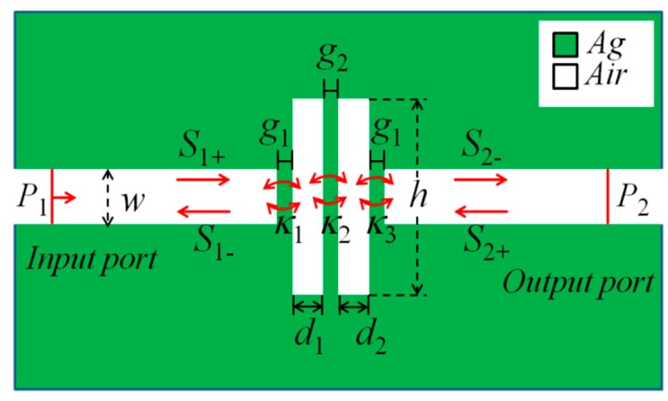
Considering that three-dimensional (3D) model simulation requires too many computer resources and the limitations of our computer workstation, the two-dimensional (2D) plasmonic waveguide coupled resonator system was investigated by the FEM in this paper. The working principle of the 2D model as similar to that of the real 3D model, because in real photonic devices if the depth of the metal layer is large enough (i.e., the third dimension much larger than the light wavelength), then the properties of the 3D model can be approximated by a 2D model. Figure 1 illustrates the geometry of the designed 2D MIM waveguide-coupled double rectangular cavity, which consists of two straight MIM waveguides with one end sealed and double rectangular cavities with a parallel arrangement. One rectangular cavity behaves as the active cavity, and the other rectangular cavity as the passive cavity. To ensure fundamental transverse magnetic (TM0) mode propagation in the MIM waveguide, the insulator layer width of the MIM waveguide was fixed at w = 50 nm [32]. The input port (P1) and output port (P2) are located in the left and the right end of the MIM waveguide, respectively. The coupling distance between the MIM waveguide and rectangular cavity is g1 (5 nm) and the gap between the double rectangular cavities is g2. The widths of the left and right rectangular cavities are d1 and d2, respectively. The height of the double rectangular cavities is h. The refractive index of the dielectric layer (white) in the MIM waveguide and rectangular cavity is denoted as n.
Figure 1.
Schematics of the proposed MIM waveguide-coupled double rectangular cavities.
The propagation properties of the MIM waveguide-coupled double rectangular cavities were simulated by the FEM. PMLs were set at the up and bottom boundaries of the structure. The frequency-dependent complex relative permittivity ε(ω) of silver is characterized by the modified Debye-Drude dispersion model [33]:
| (1) |
where the infinite permittivity ε∞ = 3.8344, static permittivity εs = −9530.5, relaxation time τ = 7.35 × 10⁻¹⁵, and conductivity σ =1.1486 × 10⁷ s/m.
For MIM waveguide coupling resonator, the resonance wavelength can be determined by [34,35]:
| (2) |
where L is the perimeter of the cavities, positive integer m is the number of antinodes of the standing SPP wave, and ψr is the phase shift of the beam reflected at one end of the cavity. Re(neff) is the real part of the effective refractive index in MIM waveguide, which can be obtained by solving the dispersion relation of the TM0 mode in a MIM waveguide.
The TM0 model equation in the MIM waveguide is [15,32]:
| (3) |
where k and d are the wave vector in the waveguide and the width of the MIM waveguide, respectively. The parameters p and αc in Equation (3) are defined as p = εin/εm and αc = [k02 (εin − εm) + κ]1/2. εin and εm are the dielectric constants of the insulator and metal, respectively. The wave vector in free space k0 = 2π/λ0. Therefore, k can be solved from Equation (3) using the iterative method. Thus, the effective index neff of the MIM waveguide can be expressed as Re(neff) = [εm + (k/k0)2]1/2. The wavelength of SPPs λspp can be obtained from λspp = λ0/Re(neff). P1 is defined as the input port, and P2 is the output port. The transmission of the MIM waveguide coupling cavity is determined as T = (S21)2, where S21 is the transmission coefficient from port 1 to port 2. In addition, FOM was used to evaluate the sensitivity of the refractive index sensor. FOM is defined as (δλ/δn)/FWHM, where δλ is the wavelength change corresponding to the refractive index change δn, and FWHM is the full width at half-maximum of the resonance peak.
For the MIM waveguide coupled double rectangular cavities system, the temporal coupled mode theory (CMT) [36,37] is utilized to analyze in detail the Fano resonance in this paper. The amplitudes of the SPPs wave of the cavity are denoted by Si ± (i = 1, 2, and 3), and the subscripts ± of Si± denote the input and output from the rectangular cavity (as shown in Figure 1), respectively. When an optical wave with a frequency ω is launched only from the input port of the MIM waveguide (S2+ = 0), the time evolution amplitude Ai ± (i = 1,2, and 3) of the cavity can be expressed as [38]:
| (4) |
| (5) |
Here κ1 and κ3 are the coupling coefficients between the MIM waveguide and rectangular cavities, and κ2 is the coupling coefficient between the left rectangular cavity and right rectangular cavity. Then we can write 1/τ1 = κ12 and 1/ τ3 = κ32 as the corresponding decay rates from the cavity to MIM waveguide, and 1/ τ2 = κ22 is the decay rate from the left cavity to right cavity (or from right cavity to left cavity), ω1 and ω2 are the resonance frequency of the left and the right resonator, respectively. j is the imaginary unit (j2 = −1). According to energy conservation. The amplitude of the input and the output waves in coupled waveguide should satisfy the following relationships:
| (6) |
| (7) |
Therefore, the transmittance of the system can be solved from Equations (4)–(7) and can be expressed as:
| (8) |
When κ2 = 0, T = 0. But κ2 ≠ 0, the coupling between double rectangular cavities significantly perturbs the wave transmitted from the left waveguide to right waveguide, which result in a complex interference phenomena, and makes the system exhibit a Fano line shape.
3. Results and Discussion
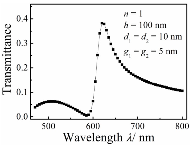
Figure 2 shows the transmission spectrum of the MIM waveguide-coupled double rectangular cavities with d1 = d2 = 10 nm, h = 100 nm, g1 = g2 = 5 nm and n = 1. A resonance peak with asymmetric line shape is observed. The slope of the left shoulder of the resonance peak is obviously larger than that of the right shoulder, which is a typical Fano profile with one maximum and one minimum. The transmittance is near to 0 at the transmission dip (λ = 580 nm). The dip is regarded as a superradiative mode but the peak as a nonoradiative mode.
Figure 2.
Transmission spectrum of the MIM waveguide-coupled double rectangular cavities.
Figure 3a,b display the normalized magnetic field Hz distributions for the transmission dip (λdip = 580 nm) and transmission peak (λpeak = 620 nm) of the MIM waveguide-coupled double rectangular cavities, respectively. For the superradiative mode (λdip = 580 nm), the Hz field distributions show that there is in-phase between the double rectangular cavities. A very weaken coupling occur between double rectangular cavities, and have no SPPs coupled into the right MIM waveguide, which agrees well with the result (κ2 = 0, T = 0) from Equation (8). For the nonradiative mode (λpeak = 620 nm), the Hz fields distribution show that there is anti-phase between double rectangular cavities. The superradiative mode is excited by the SPPs from input waveguide, the nonradiative mode cannot. However, it can be excited by the near-field associated with the superradiative mode. Fano resonances arise from the interaction between the superradiative (discrete state) mode and the nonradiative mode (continuum state).
Figure 3.
Steady state magnetic field Hz distributions for the (a) transmission dip (580 nm); and (b) transmission peak (620 nm) of the MIM waveguide-coupled double rectangular cavities.
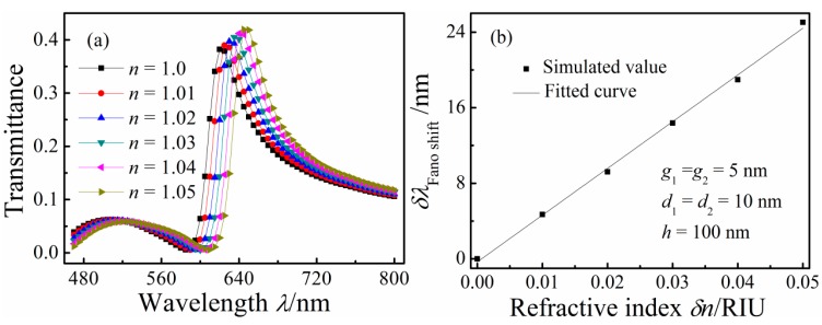
To investigate the sensitivity of the Fano resonance of the proposed nanosensor to n, dielectrics with different n were filled in the MIM waveguides and double rectangular cavities. Figure 4a depicts the transmission spectra of the MIM waveguide-coupled double rectangular cavities with n of 1–1.05 RIU in increments of 0.01 RIU; others structural parameters g1, d, h, and g2 were fixed at 5, 10, 100, and 5 nm, respectively. With increasing n, Re(neff) increased. The Fano resonance peak showed a red shift as n increased. These Fano resonance peak red shifts can also be explained using Equation (2). The transmission spectra reveal that the transmittance of the Fano resonance peak increased with increasing n. Figure 4b shows the shift of the Fano resonance peak as a function of δn. The solid curves are the linear fittings. The sensitivity δλ/δn of the refractive index sensor is 495 nm/RIU according to Figure 4b, and its FOM is 7.5.
Figure 4.
(a) Transmission spectra for different refractive index n; and (b) the shift of the Fano resonance peak as a function of the refractive index change δn.
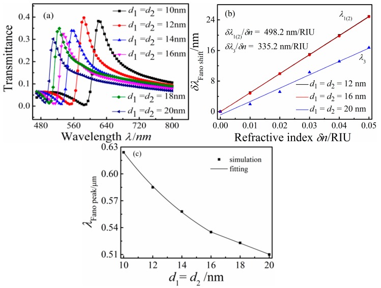
To study the effect of the double rectangular cavities widths on the Fano resonance of the MIM waveguide-coupled double rectangular cavities, d1 and d2 were increased synchronously from d1 = d2 = 10 nm to d1 = d2 = 20 nm with fixed h = 100 nm, g = g1 = 5 nm, and n = 1 RIU. The transmission spectra of the MIM waveguides coupled different double rectangular cavities widths for d1 = d2 = 10, 12, 14, 16, 18, and 20 nm are presented in Figure 5a. With increasing double rectangular cavities widths (d1 = d2), the Fano resonance of the system blue shifts obviously. This can be explained by the increase of d1 and d2 decreasing Re(neff), and the blue shift of the Fano resonance peak is also predicted by above Equation (2). Figure 5b shows the shift of the Fano resonance peak (d1 = d2 = 12, 16, and 20 nm) as a function δn. The solid curves are the linear fittings. The sensitivity δλ/δn of the nanosensor with d1 = d2 = 12 nm is equal to that of the configuration with d1 = d2 = 16 nm, with a value of 498.2 nm/RIU. Compared with the nanosensor with d1 = d2 = 12 and 16 nm, δλ/δn for the configuration with d1 = d2 = 20 nm decreases obviously to 335.2 nm/RIU. As shown in Figure 5c, the Fano resonance peak change as the widths (d1 = d2) is an exponential decay function from the d1 = d2 = 10 nm to d1 = d2 = 16 nm, but it is linear function from d1 = d2 =16 nm to d1 = d2 = 20 nm. The point (d1 = d2 = 16 nm) is a inflection point of the function of Fano peak as the d1 (d2), so an abrupt change is observed from d1 = d2 = 16 nm to d1 = d2 = 20 nm.
Figure 5.
(a) Transmission spectra for different rectangular cavity widths d1(d2); (b) the shift of the Fano resonance peak as a function of the refractive index change δn; and (c) the Fano resonance peak as a function of the rectangular cavity widths change d1(d2).
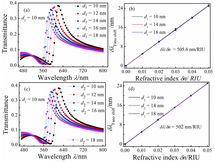
Figure 6a shows that the transmission spectra when d1 is increased from 10 to 20 nm in 2 nm increments with fixed d2 = 10 nm, h = 100 nm, g = g1 = 5 nm, and n = 1 RIU. With increasing d1, the blue shift and the transmittance of the Fano resonance peak decreased slightly. The increase of d1 caused Re(neff) to decrease in the rectangular cavity. Figure 6b shows the shift of the Fano resonance peak δλFano shift as a function of δn, from which we calculated that δλ/δn is 505.6 nm/RIU for this configuration. In addition, we fixed d1 to investigate the effect of varying d2 on the transmission spectra. Figure 6c displays the transmission spectra for systems with d2 = 10, 12, 14, 16, 18, and 20 nm with fixed d1 = 10 nm. With increasing d2, the Fano resonance peak blue shifts and its transmittance decreases slightly. Figure 6d presents δλFano shift plotted as a function of δn for the configurations with different d2; δλ/δn determined from this plot is 502 nm/RIU.
Figure 6.
(a,c) Transmission spectra for different rectangular cavities width d1 (a) and d2 (c); respectively; (b,d) the shift of the Fano resonance peak as a function of δn with different rectangular cavities width d1 (b) and d2 (d), respectively.
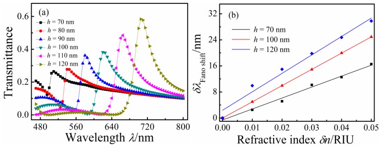
The simulation indicate that the Fano resonance peak as the changing of the refractive index is linear function, and they parallel to each other nearly for different d1 or d2, namely they have same slope. So the refractive index sensitivity δλ/δn curves overlapped each other. To investigate how h affects the Fano resonance of the MIM waveguide-coupled double rectangular cavities, transmission spectra for different height h of 80, 90, 100, 110, and 120 nm with g = g1 = 5 nm, d = 10 nm, and n = 1 RIU were calculated, and are plotted in Figure 7a. With increasing h, the Fano resonance peak red-shifted linearly because the SPPs pathway in the rectangular cavity lengthened, and its transmittance increased. Figure 7b illustrates the shift of the Fano resonance peak as a function of δn for h = 70, 100, 120 nm. The solid curve is the linear fitting. With increasing h, δλ/δn increased. For h = 70, 100, and 120 nm, δλ/δn are 331, 498, and 596 nm/RIU.
Figure 7.
(a) Transmission spectra; and (b) Fano resonance wavelengths of MIM waveguides-coupled double rectangular cavities with different double rectangular cavities heights h.
4. Conclusions
The transmission properties of MIM waveguide-coupled double rectangular cavities were studied using the FEM. A Fano resonance peak was observed in transmission spectra, and it depended on the mode coupling between the double rectangular cavities. Upon increasing the width of the double rectangular cavities simultaneously, the Fano resonance peak blue shifted and its transmittance decreased, and the sensitivity decreased. Upon increasing the width of one rectangular cavity, the Fano resonance peak blue shifted and the sensitivity did not change. The Fano resonance peak exhibited an obvious red shift and its transmittance increased with increasing height of the double rectangular cavities; the sensitivity also increased obviously. The refractive index sensitivity (596 nm/RIU) of the MIM waveguide coupled double rectangular cavities is higher than the previously [27]. The sensitivity of the proposed sensor based on waveguide coupled resonance is smaller than that of the conventional SPR sensor based on Kretschmann geometry [39], but the former is easier to integrate with various photonic devices and chips than the latter.
Acknowledgments
This work was supported by the National Natural Science Foundation of China (Grant No. 61275166), the Fund Program for the Scientific Activities of Selected Returned Overseas Professionals in Shanxi Province, the Science Foundation of North University of China (Grant No. 110246), Program for the Top Young and Middle-aged Innovative Talents of Higher Learning Institutions of Shanxi, and the North University of China Science Fund for Distinguished Young Scholars.
Abbreviations
The following abbreviations are used in this manuscript:
| SPPs | Surface plsmon polartions |
| MIM | Metal-insulator-metal |
| FEM | Finite element method |
| FOM | Figure of merit |
| PML | Perfectly matched layer |
| 3D | Three-dimensional |
| 2D | Two-dimensional |
| CMT | Coupled mode theory |
| TM0 | Fundamental transverse magnetic |
| FWHM | Full width at half-maximum |
Author Contributions
Zhi-Dong Zhang analyzed the data and wrote the paper; Zhi-Dong Zhang, Liang Luo and Shu-Bin Yan conceived and designed the simulations; Liang Luo performed the simulations; Shu-Bin Yan revised the paper; Chen-Yang Xue and Wen-Dong Zhang contributed analysis tools.
Conflicts of Interest
The authors declare no conflict of interest.
References
- 1.Barnes W.L., Dereux A., Ebbesen T.W. Surface plasmon subwavelength optics. Nature. 2003;424:824–830. doi: 10.1038/nature01937. [DOI] [PubMed] [Google Scholar]
- 2.Zayats A.V., Smolyaninov I.I., Maradudin A.A. Nano-optics of surface plasmon polaritons. Phys. Rep. 2005;408:131–314. doi: 10.1016/j.physrep.2004.11.001. [DOI] [Google Scholar]
- 3.Yin Y., Qiu T., Li J., Chu P.K. Plasmonic nano-lasers. Nano Energy. 2012;1:25–41. doi: 10.1016/j.nanoen.2011.09.002. [DOI] [Google Scholar]
- 4.Zafar R., Salim M. Achievement of large normalized delay bandwidth product by exciting electromagnetic-induced transparency in plasmonic waveguide. IEEE J. Quantum Electron. 2015;51:7200306–7200312. doi: 10.1109/JQE.2015.2472979. [DOI] [Google Scholar]
- 5.Zhang Z.D., Wang H.Y., Zhang Z.Y. Fano resonance in a gear-shaped nanocavity of the metal-insulator-metal waveguide. Plasmonics. 2012;8:797–801. doi: 10.1007/s11468-012-9475-9. [DOI] [Google Scholar]
- 6.Hakala T.K., Toppari J.J., Kuzyk A., Pettersson M., Tikkanen H., Kunttu H., Törmä P. Vacuum Rabi splitting and strong-coupling dynamics for surface-plasmon polaritons and rhodamine 6G molecules. Phys. Rev. Lett. 2009;103:053602. doi: 10.1103/PhysRevLett.103.053602. [DOI] [PubMed] [Google Scholar]
- 7.Hao J., Liu T., Huang Y., Chen G., Liu A., Wang S., Wen W. Metal nanoparticle-nanowire assisted SERS on film. J. Phys. Chem. C. 2015;119:19376–19381. doi: 10.1021/acs.jpcc.5b05690. [DOI] [Google Scholar]
- 8.Wu T., Liu Y., Yu Z., Ye H., Peng Y., Shu C., Yang C., Zhang W., He H. A nanometeric temperature sensor based on plasmonic waveguide with an ethanol-sealed rectangular cavity. Opt. Commun. 2015;339:1–6. doi: 10.1016/j.optcom.2014.11.064. [DOI] [Google Scholar]
- 9.Kashif M., Bakar A.A., Arsad N., Shaari S. Development of phase detection schemes based on surface plasmon resonance using interferometry. Sensors. 2014;14:15914–15938. doi: 10.3390/s140915914. [DOI] [PMC free article] [PubMed] [Google Scholar]
- 10.Brolo A.G. Plasmonics for future biosensors. Nat. Photonics. 2012;6:709–713. doi: 10.1038/nphoton.2012.266. [DOI] [Google Scholar]
- 11.Jiang Y., Wang H.Y., Wang H., Gao B.R., Hao Y.W., Jin Y., Chen Q.D., Sun H.B. Surface plasmon enhanced fluorescence of dye molecules on metal grating films. J. Phys. Chem. C. 2011;115:12636–12642. doi: 10.1021/jp203530e. [DOI] [Google Scholar]
- 12.Fang Y., Sun M. Nanoplasmonic waveguides: Towards applications in integrated nanophotonic circuits. Light Sci. Appl. 2015;4:e294. doi: 10.1038/lsa.2015.67. [DOI] [Google Scholar]
- 13.Chen Z., Yu L. Multiple fano resonances based on different waveguide modes in a symmetry breaking plasmonic system. IEEE Photonics J. 2014;6:1–8. doi: 10.1109/JPHOT.2014.2368779. [DOI] [Google Scholar]
- 14.Tong L.M., Wei H., Zhang S.P., Xu H.X. Recent advances in plasmonic sensors. Sensors. 2014;14:7959–7973. doi: 10.3390/s140507959. [DOI] [PMC free article] [PubMed] [Google Scholar]
- 15.Zhang Z., Wang J., Zhao Y., Lu D., Xiong Z. Numerical investigation of a branch-shaped filter based on metal-insulator-metal waveguide. Plasmonics. 2011;6:773–778. doi: 10.1007/s11468-011-9263-y. [DOI] [Google Scholar]
- 16.Wu Y.D. High transmission efficiency wavelength division multiplexer based on metal-insulator-metal plasmonic waveguides. J. Lightwave Technol. 2014;32:4844–4848. [Google Scholar]
- 17.Xie Y.Y., Huang Y.X., Zhao W.L., Xu W.H., He C.A. Novel Plasmonic sensor based on metal-insulator-metal waveguide with side-coupled hexagonal cavity. IEEE Photonics J. 2015;7:1–12. doi: 10.1109/JPHOT.2015.2419635. [DOI] [Google Scholar]
- 18.Qi J., Chen Z., Chen J., Li Y., Qiang W., Xu J., Sun Q. Independently tunable double Fano resonances in asymmetric MIM waveguide structure. Opt. Express. 2014;22:14688–14695. doi: 10.1364/OE.22.014688. [DOI] [PubMed] [Google Scholar]
- 19.Lee K.L., Huang J.B., Chang J.W., Wu S.H., Wei P.K. Ultrasensitive biosensors using enhanced Fano resonances in capped gold nanoslit arrays. Sci. Rep. 2015;5:08547–08555. doi: 10.1038/srep08547. [DOI] [PMC free article] [PubMed] [Google Scholar]
- 20.Chen J., Sun C., Gong Q. Fano resonances in a single defect nanocavity coupled with a plasmonic waveguide. Opt. Lett. 2014;39:52–55. doi: 10.1364/OL.39.000052. [DOI] [PubMed] [Google Scholar]
- 21.Chen J., Li Z., Zou Y., Deng Z., Xiao J., Gong Q. Coupled-resonator-induced Fano resonances for plasmonic sensing with ultra-high figure of merits. Plasmonics. 2013;8:1627–1631. doi: 10.1007/s11468-013-9580-4. [DOI] [Google Scholar]
- 22.Luk’yanchuk B., Zheludev N.I.S., Maier A., Halas N.J., Nordlander P., Giessen H., Chong T.C. The Fano resonance in plasmonic nanostructures and metamaterials. Nat. Mater. 2010;9:707–715. doi: 10.1038/nmat2810. [DOI] [PubMed] [Google Scholar]
- 23.Rahmani M., Luk’yanchuk B., Hong M. Fano resonance in novel plasmonic nanostructures. Laser Photonics Rev. 2013;7:329–349. doi: 10.1002/lpor.201200021. [DOI] [Google Scholar]
- 24.Miroshnichenko A.E., Flach S., Kivshar Y.S. Fano resonances in nanoscale structures. Rev. Mod. Phys. 2010;82:2257–2298. doi: 10.1103/RevModPhys.82.2257. [DOI] [Google Scholar]
- 25.Wu T., Liu Y., Yu Z., Peng Y., Shu C., Ye H. The sensing characteristics of plasmonic waveguide with a ring resonator. Opt. Express. 2014;22:7669–7677. doi: 10.1364/OE.22.007669. [DOI] [PubMed] [Google Scholar]
- 26.Yan S.B., Luo L., Xue C.Y., Zhang Z.D. A refractive index sensor based on a metal-insulator-metal waveguide-coupled ring resonator. Sensors. 2015;15:29183–29191. doi: 10.3390/s151129183. [DOI] [PMC free article] [PubMed] [Google Scholar]
- 27.Xie Y.Y., Huang Y.X., Che H.J., Zhao W.L., Xu W.H., Li X., Li J. Theoretical investigation of a plasmonic sensor based on a metal-insulator-metal waveguide with a side-coupled nanodisk resonator. J. Nanophotonics. 2015;9:093099-1–093099-13. doi: 10.1117/1.JNP.9.093099. [DOI] [Google Scholar]
- 28.Chen Z., Wang W., Cui L., Yu L., Duan G., Zhao Y., Xiao J. Spectral splitting based on electromagnetically induced transparency in plasmonic waveguide resonator system. Plasmonics. 2014;10:721–727. doi: 10.1007/s11468-014-9858-1. [DOI] [Google Scholar]
- 29.Chen Z., Song X., Jiao R., Duan G., Wang L., Yu L. Tunable electromagnetically induced transparency in plasmonic system and its application in nanosensor and spectral splitting. IEEE Photonics J. 2015;7:4801408-1–4801408-8. [Google Scholar]
- 30.Zhang S., Bao K., Halas N.J., Xu H., Nordlander P. Substrate-induced Fano resonances of a plasmonic nanocube: A route to increased-sensitivity localized surface plasmon resonance sensors revealed. Nano Lett. 2011;11:1657–1663. doi: 10.1021/nl200135r. [DOI] [PubMed] [Google Scholar]
- 31.Hayashi S., Nesterenko D.V., Sekkat Z. Waveguide-coupled surface plasmon resonance sensor structures: Fano lineshape engineering for ultrahigh-resolution sensing. J. Phys. D Appl. Phys. 2015;48:325303. doi: 10.1088/0022-3727/48/32/325303. [DOI] [Google Scholar]
- 32.Kekatpure R.D., Hryciw A.C., Barnard E.S., Brongersma M.L. Solving dielectric and plasmonic waveguide dispersion relations on a pocket calculator. Opt. Express. 2009;17:24112–24129. doi: 10.1364/OE.17.024112. [DOI] [PubMed] [Google Scholar]
- 33.Gai H., Wang J., Tian Q. Modified Debye model parameters of metals applicable for broadband calculations. Appl. Opt. 2007;46:2229–2233. doi: 10.1364/AO.46.002229. [DOI] [PubMed] [Google Scholar]
- 34.Zhu J.H., Wang Q.J., Shum P., Huang X.G. A simple nanometeric plasmonic narrow-band filter structure based on metal-insulator-metal waveguide. IEEE Trans. Nanotechnol. 2011;10:1371–1376. doi: 10.1109/TNANO.2011.2147330. [DOI] [Google Scholar]
- 35.Hu F., Yi H., Zhou Z. Wavelength demultiplexing structure based on arrayed plasmonic slot cavities. Opt. Lett. 2011;36:1500–1502. doi: 10.1364/OL.36.001500. [DOI] [PubMed] [Google Scholar]
- 36.Haus H.A. Waves and Fields in Optoelectronics. Prentice-Hall; Upper Saddle River, NJ, USA: 1984. [Google Scholar]
- 37.Haus H.A., Huang W.P. Coupled-mode theory. IEEE Proc. 1991;79:1505–1518. doi: 10.1109/5.104225. [DOI] [Google Scholar]
- 38.Piao X., Yu S., Koo S., Lee K., Park N. Fano-type spectral asymmetry and its control for plasmonic metal-insulator-metal stub structures. Opt. Express. 2011;19:10907–10912. doi: 10.1364/OE.19.010907. [DOI] [PubMed] [Google Scholar]
- 39.Roh S., Chung T., Lee B. Overview of the characteristics of micro- and nano-structured surface plasmon resonance sensors. Sensors. 2011;11:1565–1588. doi: 10.3390/s110201565. [DOI] [PMC free article] [PubMed] [Google Scholar]


