

Abstract
This paper describes the development of a miniaturized high frequency linear array that can be integrated within a core biopsy needle to improve tissue sampling accuracy during breast cancer biopsy procedures. The 64 element linear array has an element width of 14 μm, kerf width of 6 μm, element length of 1 mm and element thickness of 24 μm. The 2–2 array composite was fabricated using deep reactive ion etching of PMN-PT single crystal material. The array composite fabrication process as well as a novel high density electrical interconnect solution are presented and discussed. Array performance measurements show that the array had a center frequency and fractional bandwidth (−6 dB) of 59.1 MHz and 29.4%, respectively. Insertion loss and adjacent element cross talk at the center frequency were −41.0 dB and −23.7 dB, respectively. A B-mode image of a tungsten wire target phantom was captured using a synthetic aperture imaging system and the imaging test results demonstrate axial and lateral resolutions of 33.2 μm and 115.6 um, respectively.
Index Terms: Ultrasonic Transducer Arrays, Ultrasonic imaging, Piezoelectric Transducers, Connectors
I. Introduction
Ultrasound guidance during needle biopsy is the preferred image guidance approach for the gold standard diagnostic method of breast cancer since it is the most comfortable for the patient and does not require ionizing radiation [1], [2]. Despite the high diagnostic accuracy of core needle biopsy and vacuum assisted needle biopsy, thousands of the over 1.6 million women who undergo breast biopsy annually in the United States receive false negative diagnoses, allowing cancer progression and increasing mortality [3], [4]. The challenge of missed diagnoses however lies not with the failure of pathological analysis but with the inaccuracy of tissue sampling at the time of biopsy [5]. Since current clinical ultrasound systems cannot reliably visualize structures such as microcalcifications in the breast, which may suggest early breast carcinoma such as Ductal Carcinoma in situ (DCIS), new imaging methods to visualize these structures would be clinically beneficial to help improving sampling accuracy during breast biopsy procedures and lead to earlier diagnosis. High-frequency ultrasound imaging could allow radiologists to identify structures portending increased risk for malignancy within fatty breast tissue at the closest proximity to the lesion identified from the antecedent mammography. Clinical ultrasound imaging has been validated as an effective tool in guiding percutaneous needle procedures such as central venous catheterization and other needle biopsy procedures including transbronchial and pancreatic fine needle aspiration [6]–[8]. However, conventional low frequency (5 to 15 MHz) linear arrays for breast imaging do not provide sufficient spatial resolution needed for reliable microstructure visualization such as microcalcifications which are largely < 100 μm in size and currently available high frequency (30 to 60 MHz) array or single element transducer systems such as the VisualSonics Vevo 2100 and 770 are not clinically available (VisualSonics, Toronto, Ontario, Canada) to visualize these microstructures [9]. To enable high frequency ultrasound imaging of breast lesions, an imaging device must be developed to image breast tissue at the site of a lesion. Since transcutaneous high frequency imaging in the breast is impractical due to the high attenuation of sound at high frequencies, the array aperture must be small enough to fit within an interventional tool such as a core biopsy needle so that the imaging aperture is in close proximity to the lesion.
Since radiologist are trained to use in-plane technique during biopsy procedures, any additional imaging modalities or devices should produce complementary images within the same imaging plane. Therefore, in designing a miniaturized high frequency ultrasound array we wish to orient the azimuth axis of the array in parallel with the needle shaft so that the imaging plane is parallel with that of the external guidance probe as shown in Fig 1. The high frequency image produced by this new needle array will provide a high resolution complementary image to the physician during the procedure.
Fig 1.

Rendering of core biopsy needle (a) oriented in the in-plane technique within the imaging plane of the external guidance linear ultrasound array and (b) zoomed view of array with its imaging plane oriented parallel to that of the guidance probe.
We propose a miniaturized high frequency linear array integrated within an 11 gauge (3.05 mm diameter) core biopsy needle to provide ultra-high resolution images of breast tissue during ultrasound guided breast biopsy. Such images obtained at the lesion may allow radiologists to identify features not previously seen during conventional biopsy guidance such as microcalcifications, thus achieving more targeted biopsies and improve the diagnostic accuracy of breast cancer.
The prospect of ultrasound imaging during breast cancer biopsy has been demonstrated by Cochran et al. where the group fabricated a 15 MHz linear array that can fit within a 2 mm diameter biopsy needle [10]. This device is still limited, however, because imaging at 15 MHz cannot provide the necessary resolution to differentiate very small structures within the breast such as microcalcifications. It is thus necessary to build a significantly higher frequency array that can resolve these fine structures from within the compact housing of a biopsy needle.
In practice, a radiologist would guide the biopsy needle with integrated imaging array to the suspicious lesion using standard external ultrasound probe guidance, and once the needle is in close proximity to the lesion, the integrated array produces a high resolution picture that the radiologist then uses to target the precise point where the tissue is sampled. This paper reports on the design, fabrication and testing of a miniaturized 64-element 60 MHz 2–2 composite based linear array designed for use in a biopsy needle for biopsy guidance.
II. Methods
Each element in the 2–2 composite was composed of single crystal PMN-PT and was separated from its neighbors by epoxy. The array composite was backed by a highly attenuative conductive epoxy that served as the ground connection for each element. The array had a single, polymer coating matching layer to provide acoustic impedance matching between the array composite and the imaging medium. Array elements were connected to a transmission line mounted directly over the surface of the array and the array aperture was exposed to the imaging environment through a small rectangular cutout. This integrated array transmission line component can be mounted within a coaxial biopsy needle where it would image out through the side of the tissue sampling aperture. The array design, fabrication steps and testing results are described in the following sections.
A. 2–2 Composite Design
Various piezo composite fabrications methods have been developed for high frequency arrays and array development at 50 MHz and above. As the pursuit of ever smaller array kerf sizes was needed to achieve smaller and smaller array element pitches and kerf widths, traditional dice and fill techniques [11–13] were replaced with more advanced fabrication processes such as laser and chemical etching techniques [14]. Interdigital pair-bonding, interdigital phase-bonding and stacking methods also sought to decrease element pitch while still using existing dicing saw technology capabilities [15–18]. Capacitive- and Piezoelectric- micromachined ultrasound transducers (CMUT, PMUT) technologies have demonstrated the capability to produce transducers and their electrical interconnects using batch fabrication techniques based on those previously developed for the semiconductor industry [19], [20]. However, most of these arrays are limited to clinical imaging frequencies (2–15 MHz) and have not been validated for miniaturized high frequency array applications. A notable advancement was made by Brown et al by developing a miniaturized, forward looking 40 MHz phased array that utilized a novel electrical interconnection technique where wire bonding connected the array composite to metalized vias in a flex circuit [21]. Kerfless high frequency array development has been investigated as a fabrication method that avoids the problem of creating kerfs in the piezoelectric material and instead relies on simply patterning electrodes to create individual elements in an array at the expense of increased crosstalk between elements [22], [23]. Both thick and thin film deposition techniques have also been investigated for high frequency array development [24], [25]. More recently, deep reactive ion etching techniques were proven for high frequency array development [26], [27].
While progressively higher frequency arrays over 50 MHz have been developed including those for intravascular applications, none has considered the size constraints that may occur in the design of a clinical needle biopsy device. The challenge that we are addressing is improving breast cancer needle biopsy procedures and this requires much more demanding physical size constraints since the entire linear array and electrical connection must fit within a biopsy needle shaft.
The array design requirements as determined by the clinical need include array type, aperture size, orientation, frequency and packaging size. The array module must fit within the 11 gauge needle. A side-looking, linear array is needed in order to match existing imaging plane used for ultrasound needle guidance. This array aperture orientation enables simultaneous visualization of the lesion while continuously guiding the needle shaft throughout the procedure.
The array must have a significantly high center frequency in order to achieve the resolution needed to visualize structures not currently visible with clinical imaging systems. The imaging array center frequency was chosen to be 60 MHz to achieve axial and lateral resolution necessary to reliably visualize microcalcifications including those below 100 μm. Array geometry has been determined by the high frequency array design rules summarized by Ritter [28]. The size of the electrical interconnect to the array was the limiting factor in how many elements could be built in the array. Thus, a 60 MHz, 64-element 1D linear array was designed for this breast biopsy guidance application with an element width of 14 μm, kerf width of 6 μm, element height of 1 mm and an element thickness of 24 μm. A single matching layer of parylene was chosen for this array since a dual matching layer fabrication and assembly process was presently not feasible with this size of array and type of electrical interconnect. A parylene matching layer was relatively easy to implement since it entailed the attachment of only the polymer layer via vapor deposition but the only fabrication process for a 2nd matching layer required manually placing a 1.2 mm × 1 mm film less than 10 μm thick on the array aperture. There was not a process that could accomplish this without damaging the array composite or compromise the electrical interconnect. Thus, a single matching layer was chosen for this prototype array. Lastly, a novel electrical interconnect component and assembly fabrication process was developed specifically for this miniaturized high frequency array in order to connect it to the synthetic aperture imaging system used for performance and imaging evaluation. No commercially available imaging system existed during the development of this array and as a result we designed and built a custom synthetic aperture imaging system that enabled us to collect imaging data from the array. Fig. 2 below shows a cutaway image of the final array and Table I lists the array design parameters.
Fig. 2.

Exploded view of array acoustic stack including backing, 2–2 composite and parylene matching layer as well as zoomed view of 3 separate layers and the final assembled array unit with array dimensions given in.
TABLE I.
ARRAY DESIGN PARAMETERS
| Parameter | Value |
|---|---|
| Number of Elements | 64 |
| Element Width | 14 μm |
| Kerf Width | 6 μm |
| Element Height | 1 mm |
| Element Thickness | 24 μm |
| Matching Thickness (Parylene) | 6 μm |
| Backing Thickness (E-Solder 3022) | 1 mm |
| Focal Distance | 1.5 mm |
B. Array Composite Fabrication
The array composite, with array kerfs that are 6 m wide and 24 μm deep, was fabricated using a Deep Reactive Ion Etching (DRIE) technique optimized by Channel Technologies Group (formerly HC Materials, Bolingbrook, IL) (CTG, Santa Barbara, CA) for piezoelectric materials. This etching technique was previously used successfully for an 80 MHz, fully-kerfed ultrasound array fabrication process [29].
DRIE is an anisotropic etching process that is useful for creating microstructures out of bulk materials with especially high aspect ratios and steep sidewall angles. DRIE uses heated plasma to etch into bulk material using a photolithographically developed pattern of a hard metal such as nickel to serve as the etching mask. The high resolution of photolithography combined with the capability of DRIE to etch through materials thicker than 20 μm with very high aspect ratios (approaching 90°) makes it an ideal choice to create the small kerfs in high frequency composite arrays.
A bulk piece of PMN-(0.3)PT single crystal material made by CTG (formerly HC Materials) was lapped and polished by hand to ensure coplanarity of the top and bottom surfaces until a thickness of 1 mm was reached. This material’s bulk piezoelectric material properties were: electromechanical coupling coefficient (k33 = 0.90), dielectric constant (T33 = 6250) and tangent loss (tan < 0.008). Next, a nickel mask is patterned on to the bulk material so that the nickel is covering all of the material except for the kerf regions to be etched. Since the array size is only 1.5 mm × 1.5 mm and the piezoelectric bulk material is 15 mm × 15 mm, a 7×7 matrix of arrays can be patterned during a single batch, enabling 49 arrays to be fabricated from each bulk material sample. The reason 49 arrays were patterned on to the material is to account for the potentially low yield of undamaged and useable arrays at the end of the fabrication process. Additionally, we were interested in developing this batch fabrication method because it has much more potential as a reliable fabrication approach than traditional array fabrication processes which allow for only 1 array to be fabricated by hand at one time.
First, the 49 array composite patterns were made by spinning on and developing photoresist over the bulk PMN-PT material. Then, a layer of nickel was deposited and the photoresist was removed leaving the nickel patterned over all the piezoelectric pillars of the array composite. With the nickel masked patterned, the sample is run through the DRIE process developed by CTG (formerly HC Materials) Materials to etch down 30 μm into the bulk PMN-PT material. Etching past the designed composite thickness of 24 μm was necessary to allow for several microns of material to be removed in the subsequent lapping fabrication steps. Each element was etched into 10 sub-elements with a pitch of 100 μm and sub-element kerf width of 5 μm. This sub-element design was implemented to mitigate the risk of element electrodes breaking along their narrow length due to strain induced from expansion of the composite pillars. This design also prevented a crack from propagating across entire element composed of single crystal PMN-PT.
After DRIE processing, scanning electron micrographs of the composites shown in Fig. 3 were captured to verify the successful etch of the bulk material. Array elements are stacked vertically in this image with each element divided into 10 sub-elements and arranged along each row. Each row is one of 64 single elements in the composite.
Fig. 3.

Scanning electron microscope images of PMN-PT material obtained immediately after DRIE processing. Each complete element (b) had 10 sub-elements (a) per active element in the array. The sub-element pitch was 100 μm with a sub-element length of 95.5 μm and a sub-element kerf width of 5 μm.
In addition to the array element and sub-element kerfs, the region surrounding the 64 elements was etched away as this would be the location of the individual element electrode bonding pads and patterning these pads on top of active piezoelectric material would cause unwanted resonances that would interfere with the operation of the active elements. After DRIE processing, each composite had non-conductive, degassed epoxy (EPOTEK-301, Epoxy Technology, Inc., Billerica, MA) permeate in between the composite pillars until it completely fills the kerf space between the elements [30]. The epoxy is cured overnight in a dry box at room temperature and then post cured at 40°C for 2 hours. The bulk sample is then lapped down to expose the top of the composite pillars. The final composite had a kerf width of 6 μm and a net piezoelectric volume fraction of 67%.
C. Array Module Fabrication
After the array pillars are lapped to a fine finish, photoresist is spun down on to the sample and the individual electrode patterns are exposed and developed creating an electrode mask. Chrome/gold electrodes were then sputtered on to the composite, photoresist was then removed revealing individual element electrodes (width = 14 μm) and bonding pads (diameter = 50 μm). Once the individual elements have been patterned on to the composite, the bulk material is flipped over, wax bonded onto a carrier wafer and then lapped down until the backside of the composite pillars is exposed and the designed composite thickness of 24 μm is reached. Once the composite is at the final thickness, a common ground chrome/gold electrode is sputtered onto the entire composite surface. Next, a conductive backing is added to the array composites with E-Solder 3022, a conductive epoxy material [30]. E-Solder 3022 is cast on the common ground electrode and centrifuged at 3000 RPM for 15 minutes, then cured overnight in a dry box at room temperature, followed by a 2-hour post-cure at 40°C. The backed array composite sample is then removed from the carrier wafer, turned over and wax bonded onto a square glass carrier block exposing what will be the front surface of the array. Each individual array module is then separated from the sample with a TCAR864-1 dicing saw (Thermocarbon, Inc., Casselberry, FL) by cutting the modules in a grid pattern as shown in Fig. 4.
Fig. 4.

Individual arrays diced from (a) grid of 49 arrays to separate them (b), yielding individual arrays (c) 1.5 mm × 1.5 mm in size.
The acoustic stack layer material and acoustic properties for each array module are listed in Table II.
TABLE II.
Acoustic Stack Properties
D. Array Interconnect Solution
A new electrical interconnect solution was developed to serve as both a high density interconnect to the 64 array element bonding pads and an electrical impedance matching circuit to match the high impedance of the array elements to the standard 50 Ω impedance of the multiplexer and pulser/receiver electronics. This interconnect solution was comprised of both a compact microstrip glass transmission line and impedance matching PCB. The microstrip transmission line had a designed electrical impedance magnitude of 350 Ω to match that of each individual array element. The impedance matching PCB connected to the microstrip transmission line through a thin high-density, high frequency matrix interposer board (HCD, Sunnyvale, CA) and contained a wideband transformer circuit (Coilcraft, Cary, Illinois) with a 1:9 impedance ratio for each of the 64 array channels. The average and standard deviation of the measured impedance of the assembled array-transmission line component was 408.4 Ω and 13.0 Ω, respectively, giving an average matched impedance of 45.3 Ω at the output of the PCB where it connected through the multiplexer to the pulser/receivers. The higher than expected impedance may be attributed to thinner than expected metallization of the transmission line trace metal thickness or perhaps increased impedance through the connection between the array bonding pads and transmission line.
This novel electrical interconnect solution was chosen for this high frequency miniaturized array because of its capability to match the electrical impedance magnitude of the individual array elements and for its compact design. A major design constraint is the size of the transmission line since it needs to fit within the shaft of a biopsy needle and since all 64 channels need to be routed through this electrical interconnect, the 1 μm thick copper channel traces needed to be patterned with a very fine pitch (≤ 25 μm) on a single layer with the width not exceeding 3 mm and span 3 cm to make this a viable interconnect solution to be housed within a biopsy needle. This transmission line length was deliberately chosen since each transmission line was built on a 5” wafer and extending the length of the transmission line beyond its current length would be impractical since the substrate thickness was <200 μm. Fabricating long, narrow stem lengths, especially those in the clinical range (5–13 cm) are extremely difficult to fabricate on thin wafers since the yield is so low because of fracturing and trace metal defects. In futures version of the array the transmission line substrate material may be changed to multilayer polyimide flex so that the extended length is no longer a problem. Each copper trace on the glass transmission line is 10 μm wide with a 15 μm space between neighboring traces. The ground layer on the bottom of glass was one uniform 2 μm thick copper layer. Future versions that employ multilayer transmission line designs could reduce this width even further for smaller gauge biopsy needles as well as extend the needle length to clinically useful lengths without compromising signal power loss or signal path isolation. A small rectangular cutout was laser cut into the end of the glass transmission line where the channel traces terminated in 50 μm diameter bonding pads lined up on the edge of the cutout. These bonding pads would match face to face with the bonding pads on the array surface with the cutout providing the array aperture with an unobstructed view of the imaging environment.
The glass transmission line, its substrate material properties, and PCB are shown in Fig. 5. The PCB has a large matrix of MCX connectors at the top for coaxial cable connection to the multiplexer and a small matrix of connectors at the bottom to connect to the individual channels of the transmission line through the high density interposer board. Each transmission line was made via a wafer fabrication process with a 5” glass wafer substrate and had a final thickness of 200 μm where the glass material properties are listed in Table III.
Fig. 5.
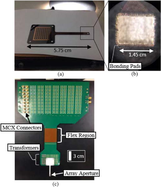
Image of (a) single microstrip transmission line laser cut from wafer with copper traces shown on top layer. Array bonding pads shown around rectangular cutout (b) match array element bonding pad pattern. The PCB (c) with individual transformer circuits for electrical impedance matching for array channels connects to the transmission line via a high density interposer board.
TABLE III.
Transmission Line Glass Material Parameters
| Parameter | Value |
|---|---|
| Dielectric Constant | 6.575 |
| Tangent Loss | 0.0086 |
| Coefficient of Thermal Expansion (glass state) | 10 ppm/K |
| Thermal Conductivity (glass state) | 1.5 W/mK |
| Electrical Resistivity | x 1012 Ω - cm |
| Tg (glass transition) | 452 °C |
| Young’s Modulus | ~78 GPa |
Due to the small size of each array module (1.5 mm × 1.5 mm × 1 mm) a novel interconnect solution between all 64 transmission line and array element channels was developed. Various, standardized interconnect methods including wire bonding and flip chip technology were unsuitable because of the demanding size, pressure, temperature and handling constraints this miniaturized array presented. The thin, fragile, epoxy-filled composite prevented any processes that required the use of elevated temperatures or pressure. Elevated temperatures would warp the composite which would develop gaps between elements and surrounding epoxy or cause breaks in the thin gold element electrodes due to expansion and contraction and applying pressure during bonding would break the fragile glass transmission line. Most of these high density interconnect solutions were developed for the semiconductor industry and even the vendors who specialize in custom interconnect solutions were unable to meet the requirements that we had.
Therefore, we developed a hybrid interconnect solution that combined components from anisotropic film connectors and conductive epoxies with flip chip and solder bumping application techniques. The solution was to use conductive microspheres and conductive epoxy to make connections between all 64 channels in a fashion similar to standard solder-based flip chip bonding.
In this new process, each array element bonding pad has a small dome-shaped conductive epoxy bumped onto it. Each of these bumps gives the bonding pad a raised profile so that its connection to the mirrored bonding pad on the transmission line can be made. The conductive epoxy was 2 – 3 μm diameter silver particles (Sigma Aldrich, St. Louis, MO) mixed with Insulcast 501 epoxy in a 2:1 weight ratio. Each epoxy bump was 25 μm – 40 μm in height and was applied with a 3-axis manual positioner stage. Next, one conductive microsphere with a diameter of 28 μm – 32 μm (Cospheric, Santa Barbara, CA) was placed on each conductive epoxy bump. These conductive spheres are manufactured in bulk and designed to be integrated into anisotropic conductive films (ACF) products that allow circuit lines to be connected in the vertical direction, but are spaced in the lateral direction to be electrically insulating along the plane of the adhesive. Each conductive microsphere has a solid soda glass core and 75 nm thick pure silver outer surface coating. We have repurposed these conductive microspheres for use as a new type vertical electrical interconnect scheme similar to flip chip bonding which does not require pressure or heat to be applied for permanent plane-to-plane circuit bonding to occur. The epoxy provides both the mechanical support to the conductive microsphere to hold it in place while also providing a conductive pathway since it is loaded with silver particles.
The conductive epoxy was allowed to cure overnight to secure the conductive microspheres in place. Next, another bump of conductive epoxy is placed on top of each conductive sphere now bonded to each bonding pad of the array in the same fashion described above. Finally, a custom 3-axis manual positioner stage is used to align the bonding pads on both the array and transmission line and lower the transmission line pads until they are in contact with the conductive microspheres. Now each bonding pad is connected via conductive microspheres with the conductive epoxy connecting the bonding pads to the conductive microspheres. This connection technique enabled the array to be connected to the transmission line at room temperature, without any pressure being applied to the delicate array module and glass transmission and without expanding the footprint of the connection, which is critical to maintaining a compact connection scheme for this array. This connection scheme is shown below in Fig. 6. The array aperture is exposed to the imaging environment through a small rectangular cutout in the glass transmission line. The ground connection between the glass transmission line and the conductive backing of the array is made with a 1 mm wide flexible strip of silver and is secured using E-Solder 3022 conductive epoxy.
Fig. 6.

Cross-sectional view of interconnect scheme between array and glass transmission line. Silver-coated glass spheres bonded by conductive epoxy were used to connect bonding pads on both the array module and transmission line.
E. Synthetic Aperture Imaging System Design
To perform imaging experiments with this array we built a synthetic aperture imaging system where a multiplexer enables a single channel pulser and single channel receiver to collect pulse-echo signals from any transmit-receive element pair in the 64 element array; the system block diagram is shown in Fig. 7.
Fig. 7.

Synthetic aperture imaging system design for high frequency array imaging.
A LabVIEW (National Instruments, Austin, TX) program running on a PC controls a multiplexer that regulates which array elements are used for transmit and receive channels during the image data capture sequence. A single channel transmit pulser and receiver were independently connected to the multiplexer. The 2×64 multiplexer was a modular NI PXIe 2593 multiplexer system (National Instruments, Austin, TX), shown in Fig. 8, which is a configurable multiplexer platform that uses computer controlled mechanical switches to channel high voltage signals within the 500 MHz bandwidth. This enabled the system to transmit and receive independently on all 64 elements of the ultrasound array. This is necessary for the synthetic aperture imaging system we implemented for image data acquisition.
Fig. 8.

Multiplexer (a) provides independent switching between transmit and receive channels with its (b) performance characteristics.
This imaging system has the capability to transmit and receive on independent channels and for each image capture and echo data was captured from each of the 64 × 64 = 4096 transmit/receive pairs. For each echo signal, each individual element was excited using a high voltage pulser and echo signals were received with an individual element, resulting in 4096 transmit/receive signals. These signals were then processed using a synthetic aperture image reconstruction technique demonstrated by Trots et al. [31]. This reconstruction method calculates the delay of each transmit/receive pair to obtain the signal at each pixel in the image field. To calculate the delay between transmit and receive elements in the array the expression is
| (1) |
Where τm and the τn is the path delay from the transmit and receive element, respectively, to the focal point in the imaging field. Where τm and the τn are described by:
| (2) |
where the point in the image field is given by (r, θ) where r is the distance between the center of the array and the point and θ is the angle of line from the center of the array this point. Furthermore, xm and xn are the positions of the m-th and n-th elements, respectively. The summed echo signal A(t) for each pixel in the image field is given by:
| (3) |
where τm,n is the delay for the (m, n) transmit and receive combination as given in (1) and ym,n(t) is the received echo signal [31]. A diagram of the transmit and receive delays calculated in (2) is shown in Fig. 9 and illustrates how each independent transmit receive pair for each individual pixel position can be simply calculated.
Fig. 9.

Diagram of path length between transmit and receive element for synthetic aperture imaging.
A MATLAB script (MathWorks, Natick, MA) was written to calculate the summed echo signal for each transmit and receive pair for every pixel position in the imaging field. Summed echo signals were then processed using envelope detection and log compressed and displayed in a grayscale B-Mode image.
F. Array Characterization
In addition to image formation there are several array transducer testing experiments that can provide insight into its performance. Array element electrical impedance and pulse/echo performance were measured prior to performing 64-channel synthetic aperture imaging. Electrical impedance was measured with an Agilent E4991A RF Impedance/Material Analyzer (Agilent Technologies, Santa Clara, CA) and both magnitude and phase angle were recorded over the frequency range of the transducer pass-band. Pulse/echo testing is useful to determine the effective bandwidth of array transducers as well as sensitivity, pulse length and focal depth. This test was performed in de-ionized water with a polished quartz reflector as the target at a distance of 2.2 mm. The pulser used for pulse/echo echo testing was a Panametrics 5900PR pulser/receiver (Panametrics, Inc., Waltham, MA) which emitted a unipolar 100 Vpp pulse. To receive echo signals a bandpass filter (10–100 MHz) and gain of 26 dB was applied before analog signals were digitized using a GaGe digitizer (Dynamic Signals, LLC, Lockport, IL) with a 1 GHz sampling rate.
For each pulse/echo time domain signal the −6 dB bandwidth was calculated using a fast fourier transform (FFT) where the lower and upper bandwidth edges were determined by the frequencies where the power spectrum was equal to −6 dB relative to the maximum value. The center frequency was taken as the midway point between the lower and upper limits of the −6 dB bandwidth. Echo amplitude was recorded for sensitivity and insertion loss comparisons. The −6 dB signal pulse length was determined by measuring the time between the first and last points where the signal was −6 dB relative to the maximum echo signal value.
The level of acoustical and electrical separation between neighboring array elements was determined by measuring cross talk between a representative element and its 3 adjacent elements. To perform this test the array was submerged in a degassed and deionized water bath. A Tektronix arbitrary waveform generator (Tektronix, Beaverton, OR) generated a signal burst to excite one element in the array with the applied voltage measured as a reference to the measured signal from adjacent elements. The signal voltage at the 3 neighboring elements is measured and compared to the reference voltage at discrete frequencies over the bandwidth of the array.
Insertion loss was measured by exciting a single element with a 60 MHz single-cycle signal, and receiving the echo off of a polished quartz target located at the focal point of the transducer. The measured amplitude value was corrected for loss due to attenuation in water and from reflection off a polished quartz target [32].
The array was used to image a single 20 μm tungsten wire target (California Fine Wire Company, Grover Beach, CA) in a de-ionized water bath. For the imaging test an AVTech AVB2-C-USCC Monocycle Pulse Generator was used to generate a 70 MHz single cycle pulse with an amplitude of 160 Vpp. Line-spread functions of the wire echo signal from the center of the wire were evaluated to determine the axial and lateral resolution of the array.
III. Results And Discussion
The results for individual array element testing are given in Table IV below. The array had no shorted or open elements, however 7 elements had very low sensitivity with insertion loss values over −60 dB. Fig. 10 shows the electrical impedance magnitude and phase angle values for one selected array element. The measurement was made at the point of the transmission line interconnect pad where it connected to the PCB, which took into account the impedance matching microstrip transmission line of each individual element channel. While the trace lengths were designed in the transmission line and PCB to be as similar as possible and the trace metallization designed to be identical, the variation in lengths or deviations in the trace metal thickness may account for the variation in impedance magnitude measurements since there was a slight trend towards lower impedance as the element number increased and also some random variable between even adjacent elements.
TABLE IV.
Average Measured Properties Of 64-Element Array
| Property | Value (Avg, StDev) |
|---|---|
| Number of Elements | 64 |
| Center frequency | 59.1 MHz, 2.5 MHz |
| Bandwidth (−6 dB) | 29.4 %, 4.0 % |
| Sensitivity | 703 mV, 381 mV |
| Insertion loss | −41.0 dB, 7.9 dB |
| Electrical impedance magnitude* | 408.4 Ω, 13.0 Ω |
| Electrical impedance phase angle* | −70.0°, 5.8° |
| Focal point | 2.2 mm |
Electrical impedance magnitude and phase angle measurements were made at 60 MHz.
Fig. 10.

Measured electrical impedance magnitude (solid line) and phase angle (dashed line) for a typical array element.
One potential cause of the extraneous mode observed in Fig. 10 is from a lateral mode in each of the element pillars which have a height of 24 μm and width of 14 μm. This could negatively affect the imaging performance because of the potential to introduce spurious signals and steps to avoid this may include decreasing the element width relative to the height to avoid any lateral resonance modes.
The average and standard deviation of the array elements center frequency and −6 dB bandwidth was (59.1 MHz, 2.5 MHz) and (29.4 %, 4.0 %), respectively. Pulseecho measurement results for a typical single element are shown in Fig. 11. The selected element #60 had a peak-to-peak voltage of 704 mV, center frequency of 59.6 MHz, bandwidth of 34.7% and −6 dB pulse length of 48 ns. Element #60 was chosen as a typical, representative element since its performance characteristics were closest to the average of all 64 elements. There was a significant variation in the sensitivity of the elements with 6 elements exhibiting sensitivity between 45 mV and 95 mV. However, the element center frequencies were more closely grouped with the minimum and maximum center frequency of 55.1 MHz and 63.7 MHz, respectively. The larger variation in sensitivity values versus center frequency suggests that variations in the electrical interconnects and traces account for the difference in performance between elements rather than differences in array element geometry because of the composite fabrication process. This array employed new array fabrication and electrical interconnect methods and it is likely that small defects in the metallization of the element electrodes reduced the effective element size or caused increased resistance in the signal path, thus decreasing the element sensitivity. Another possible issue is that defects in the array-transmission line interconnect or transmission line itself that formed during array performance characterization experiments significantly increased the channel resistance of the elements with low sensitivity. The bandwidth may have been limited by acoustic impedance mismatching between the piezoelectric element and the single parylene matching layer and in order to improve the imaging resolution of the array a second matching layer may be added.
Fig. 11.
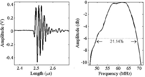
Pulse/Echo measured results for a typical array element including the (a) echo and (b) FFT magnitude plot.
Overall performance of the array uniformity in terms of center frequency, bandwidth and electric impedance magnitude and phase angle values is illustrated in Fig. 12 and Fig. 13, respectively.
Fig. 12.

Center frequency and bandwidth values for each element in array.
Fig. 13.

Impedance magnitude and phase angle values for each element in array.
The crosstalk measurements taken were consistent across the effective bandwidth of the array and the lower cross talk for elements farther away from the reference element is as expected. The measured crosstalk at the center frequency for the 1st, 2nd and 3rd nearest elements was −23.7 dB, −28.8 dB, −35.9 dB, respectively. The measured crosstalk values are shown in Fig. 14. The relatively high crosstalk level (> −30 dB) in the first 1st and 2nd adjacent elements was likely due acoustic or mechanical cross-coupling between elements in the 2–2 composite through the narrow (6 μm wide) epoxy-filled kerfs. Another possible source of the crosstalk is likely the electrical cross-coupling between both the element electrodes and the high-impedance traces in the transmission line. In future versions of this miniaturized high frequency array, cross talk may be reduced by adding a particles to the kerf filling epoxy to increase attenuation or by improving the electrical isolation of the high impedance traces on the transmission line by increasing the spacing between traces and using multilayer transmission lines with ground layers separating trace layers.
Fig. 14.

Measured crosstalk values for 3 nearest neighboring elements in array.
The measured insertion loss for a typical array element was −45.5 dB and −41.0 dB before and after correction for attenuation using the method described by Lockwood et al [32]. This value is higher than other high frequency ultrasound arrays built using micromachining fabrication methods, however, the element size in this array was 6.9 times smaller than elements in the 2 comparable arrays previously tested [26], [27]. The significantly smaller array size coupled with the single matching layer used in this array explains why the insertion loss measured was higher than what was observed in these other arrays. Improving both the electrical interconnect method and transmission line fabrication process as well as adding a second matching layer in the next generation of this array will help improve sensitivity and decrease insertion loss.
An image of the 20 μm wire test phantom is shown in Fig. 15 using a linear gray scale and 25 dB dynamic range. Image reconstruction did not include any thresholding or apodization. The line spread functions for the axial and lateral resolution plots for the center of the wire are shown in Fig. 16. The measured full-width half-maximum (FWHM) axial and lateral resolutions were 33.2 μm and 115.6 um, respectively. Faint artifacts are observed to the left and directly below the wire position. Using apodization could reduce the sidelobes but this would come at the expense of increasing the main lobe width [33]. Additionally, it is possible that the artifacts are due to in part by reflections off the thin sidewall of the rectangular glass transmission line cutout that frames the array aperture. This 1-wire phantom target image with 25 dB dynamic range demonstrates that this miniaturized high frequency linear array is functional and the fabrication and electrical interconnect methods used to produce this device are feasible.
Fig. 15.

Reconstructed synthetic aperture image of a single 20 μm wire target with no thresholding or apodization. The image was displayed with 25 dB dynamic range and mapped on a linear gray scale.
Fig. 16.

Axial (a) and lateral (b) line plots for the center of the wire phantom.
While the axial resolution is an improvement over previously reported high frequency linear arrays, the lateral resolution is not and this lower than desired lateral resolution may be improved by improving the alignment mechanism for imaging experiments. The extremely small array aperture size (1 mm × 1.2 mm) makes the fine adjustments and alignments of any phantom target difficult. Even a small deviation in the angle of the wire target from parallel alignment with the array elements elevation axis would negatively affect the lateral resolution measurement of the array.
IV. Conclusions
This paper describes the design, fabrication and testing of a 60 MHz miniaturized linear array using DRIE micromachining fabrication techniques. The array is intended to be integrated into a breast core biopsy needle. The array characterization and image formation testing served as a successful proof of concept for the new array fabrication and electrical interconnect assembly processes. The axial resolution was acceptable and steps to improve the lateral resolution may include increasing the aperture size and improving the bandwidth of the array elements by adding a second matching layer. Improving the array element uniformity and performance and implementing a more robust and simple electrical interconnect solution are the focus of the future work for this miniature high frequency array development. This array fabrication and testing confirmed that the most challenging aspect of fabricating this type of array is the connection of the miniature high frequency ultrasound array to the imaging system and future development paths include using micromachining technologies to make even simpler, smaller and easier to process interconnect components. Developing robust high density electrical interconnect solutions for this high frequency array and improving acoustic properties of array elements will be critical for progressing towards clinical applications for this array since relying on polyimide flex circuit technology for a single layer transmission line will not be feasible due to the fine trace and space of the channels. In the future, this type of miniaturized high frequency array has the potential to improve tissue visualization during breast biopsy procedures, making tissue sampling more accurate and thus increasing the accuracy of breast cancer diagnosis.
Acknowledgments
This work was supported by the NIH through the grant: P41-EB002182 and also by the NIH’s National Cancer Institute through the grant: P30CA014089.
References
- 1.Parker SH, Burbank F, Jackman RJ, Aucreman CJ, Cardenosa G, Cink TM, Coscia JL, Jr, Eklund GW, Evans WP, 3rd, Garver PR. Percutaneous large-core breast biopsy: a multi-institutional study. Radiology. 1994;193(2):359–364. doi: 10.1148/radiology.193.2.7972743. [DOI] [PubMed] [Google Scholar]
- 2.O’Flynn EAM, Wilson ARM, Michell MJ. Image-guided breast biopsy: state-of-the-art. Clin Radiol. 2010;65(4):259–270. doi: 10.1016/j.crad.2010.01.008. [DOI] [PubMed] [Google Scholar]
- 3.Youk JH, Kim EK, Kim MJ, Lee JY, Oh KK. Missed Breast Cancers at US-guided Core Needle Biopsy: How to Reduce Them. Radiographics. 2007;27(1):79–94. doi: 10.1148/rg.271065029. [DOI] [PubMed] [Google Scholar]
- 4.American Cancer Society. Cancer Facts & Figures 2015. American Cancer Society. 2015 [Google Scholar]
- 5.Bruening W, Schoelles K, Treadwell J, Launders J, Fontanarosa J, Tipton K. Comparative effectiveness of core-needle and open surgical biopsy for the diagnosis of breast lesions. Agency for Healthcare Research and Quality. 2009 [PubMed] [Google Scholar]
- 6.Karakitsos D, Labropoulos N, De Groot E, Patrianakos AP, Kouraklis G, Poularas J, Samonis G, Tsoutsos DA, Konstadoulakis MM, Karabinis A. Real-time ultrasound-guided catheterisation of the internal jugular vein: a prospective comparison with the landmark technique in critical care patients. Crit Care Med. 2006;10(6):R162. doi: 10.1186/cc5101. [DOI] [PMC free article] [PubMed] [Google Scholar]
- 7.Herth FJ, Eberhardt R, Vilmann P, Krasnik M, Ernst A. Real-time endobronchial ultrasound guided transbronchial needle aspiration for sampling mediastinal lymph nodes. Thorax. 2006;61(9):795–798. doi: 10.1136/thx.2005.047829. [DOI] [PMC free article] [PubMed] [Google Scholar]
- 8.Williams DB, Sahai AV, Aabakken L, Penman ID, Van Velse A, Webb J, Wilson M, Hoffman BJ, Hawes RH. Endoscopic ultrasound guided fine needle aspiration biopsy: a large single centre experience. Gut. 1999;44(5):720–726. doi: 10.1136/gut.44.5.720. [DOI] [PMC free article] [PubMed] [Google Scholar]
- 9.Soo MS, Baker JA, Rosen EL. Sonographic detection and sonographically guided biopsy of breast microcalcifications. Am J Roentgenol. 2003;180(4):941–948. doi: 10.2214/ajr.180.4.1800941. [DOI] [PubMed] [Google Scholar]
- 10.Flynn D, Amalou F, Parry J, McAneny J, Button TW, Desmulliez MPY, Cochran S. Progress towards wafer-scale fabrication of ultrasound arrays for real-time high-resolution biomedical imaging. Sensor Review. 2009;29(4):333–338. [Google Scholar]
- 11.Cannata JM, Shung KK. A comparison of model and experiment for a high frequency (35 MHz) linear ultrasonic array. Proc IEEE Ultrason Symp. 2003;2:1658–1662. [Google Scholar]
- 12.Cannata JM, Williams J, Zhou Q, Ritter T, Shung KK. Development of a 35-MHz piezo-composite ultrasound array for medical imaging. IEEE Trans Ultrason Ferroelect Freq Control. 2006;53(1):224–236. doi: 10.1109/tuffc.2006.1588408. [DOI] [PubMed] [Google Scholar]
- 13.Savakas HP, Klicker KA, Newnham RE. PZT-epoxy piezoelectric transducers: A simplified fabrication procedure. Mater Res Bull. 1981;16(6):677–680. [Google Scholar]
- 14.Lukacs M, Sayer M, Foster FS. Single-element and linear array transducer design for ultrasound biomicroscopy. Proc Med Imaging: Ultrason Transd Eng. 1998;3341:272–282. 1998. [Google Scholar]
- 15.Liu R, Harasiewicz KA, Foster FS. Interdigital pair bonding for high frequency (20–50 MHz) ultrasonic composite transducers. IEEE Trans Ultrason Ferroelect Freq Contr. 2001;48(1):299–306. doi: 10.1109/58.896143. [DOI] [PubMed] [Google Scholar]
- 16.Yin J, Lukacs M, Harasiewicz K, Foster FS. Ultra-fine piezoelectric composites for high frequency ultrasonic transducers. Proc IEEE Ultrason Symp. 2004;3:1962–1965. [Google Scholar]
- 17.Ritter TA, Gerber E, Shung KK, Shrout TR. Method for manufacture of high frequency ultrasound transducers. 6 183 578. US Patent. 2001 Feb 6;
- 18.Hackenberger W, Kwon S, Rehrig P, Snook K, Rhee S, Geng X. 2–2 PZT-polymer composites for high frequency (>20 MHz) ultrasound transducers. Proc IEEE Ultrason Symp. 2002;2:1253–1256. [Google Scholar]
- 19.Oralkan O, Ergun AS, Cheng CH, Johnson JA, Karaman M, Lee TH, Khuri-Yakub BT. Volumetric ultrasound imaging using 2-D CMUT arrays. IEEE Trans Ultrason Ferroelect Freq Control. 2003;50(11):1581–1594. doi: 10.1109/tuffc.2003.1251142. [DOI] [PubMed] [Google Scholar]
- 20.Khuri-Yakub BT, Oralkan Ö. Capacitive micromachined ultrasonic transducers for medical imaging and therapy. J Micromech Microeng. 2011;21(5) doi: 10.1088/0960-1317/21/5/054004. [DOI] [PMC free article] [PubMed] [Google Scholar]
- 21.Bezanson A, Adamson R, Brown JA. Fabrication and performance of a miniaturized 64-element high-frequency endoscopic phased array. IEEE Trans Ultrason Ferroelect Freq Control. 2014;61(1):33–43. doi: 10.1109/TUFFC.2014.6689774. [DOI] [PubMed] [Google Scholar]
- 22.Zhu B, Chan NY, Dai J, Shung KK, Takeuchi S, Zhou Q. New fabrication of high-frequency (100-MHz) ultrasound PZT film kerfless linear array [Correspondence] IEEE Trans Ultrason Ferroelect Freq Control. 2013;60(4):854–857. doi: 10.1109/TUFFC.2013.2635. 2013. [DOI] [PMC free article] [PubMed] [Google Scholar]
- 23.Chen R, Cabrera-Munoz NE, Lam KH, Hsu HS, Zheng F, Zhou Q, Shung KK. PMN-PT single-crystal high-frequency kerfless phased array. IEEE Trans Ultrason Ferroelect Freq Control. 2014;61(6):1033–1041. doi: 10.1109/TUFFC.2014.2999. [DOI] [PMC free article] [PubMed] [Google Scholar]
- 24.Zhang JY, Ji XM, Zhou J, Huang YP, Xu WJ, Carlier J, Gao JM, Nongaillard B. A novel method to fabricate full-kerfed high frequency (> 100 MHz) ultrasonic array transducers. Ultrason Symp (IUS) IEEE Intern. 2011:1739–1742. [Google Scholar]
- 25.Ito Y, Kushida K, Sugawara K, Takeuchi H. A 100 MHz ultrasonic transducer array using ZnO thin films. IEEE Trans Ultrason Ferroelect Freq Contr. 1995;42(2):316–324. [Google Scholar]
- 26.Zhou Q, Wu D, Liu C, Zhu B, Djuth F, Shung KK. Micro-machined high-frequency (80 MHz) PZT thick film linear arrays. IEEE Trans Ultrason Ferroelect Freq Control. 2010;57(10):2213–2220. doi: 10.1109/TUFFC.2010.1680. [DOI] [PMC free article] [PubMed] [Google Scholar]
- 27.Liu C, Zhou Q, Djuth FT, Shung KK. High-frequency (> 50 MHz) medical ultrasound linear arrays fabricated from micromachined bulk PZT materials. IEEE Trans Ultrason Ferroelect Freq Control. 2012;59(2):315–318. doi: 10.1109/TUFFC.2012.2193. [DOI] [PMC free article] [PubMed] [Google Scholar]
- 28.Ritter T. PhD dissertation. Dept. of Bioeng., Penn. State Univ.; State College, PA: 2000. Design, Fabrication and Testing of High frequency (>20 MHz) Composite Ultrasound Imaging Array. [Google Scholar]
- 29.Liu C, Djuth FT, Zhou Q, Shung KK. Micromachining techniques in developing high-frequency piezoelectric composite ultrasonic array transducers. IEEE Trans Ultrason Ferroelect Freq Control. 2013;60(12):2615–2625. doi: 10.1109/TUFFC.2013.2860. [DOI] [PMC free article] [PubMed] [Google Scholar]
- 30.Wang H, Ritter TA, Cao W, Shung KK. Passive materials for high-frequency ultrasound transducers. Med Imaging 1999: Ultrason Trans Eng. 1999:35–42. doi: 10.1109/58.895911. [DOI] [PubMed] [Google Scholar]
- 31.Trots I, Nowicki A, Lewandowski M. Synthetic transmit aperture in ultrasound imaging. Arch Acoust. 2009;34(4):685–695. [Google Scholar]
- 32.Lockwood GR, Turnbull DH, Foster FS. Fabrication of high frequency spherically shaped ceramic transducers. IEEE Trans Ultrason Ferroelect Freq Control. 1994;41(2):231–235. [Google Scholar]
- 33.Frazier CH, Brien W. Synthetic aperture techniques with a virtual source element. IEEE Trans Ultrason Ferroelect Freq Control. 1998;45(1):196–207. doi: 10.1109/58.646925. [DOI] [PubMed] [Google Scholar]