Abstract
In this work, we designed a sensitivity-enhanced surface plasmon resonance biosensor structure based on silicon nanosheet and two-dimensional transition metal dichalcogenides. This configuration contains six components: SF10 triangular prism, gold thin film, silicon nanosheet, two-dimensional MoS2/MoSe2/WS2/WSe2 (defined as MX2) layers, biomolecular analyte layer and sensing medium. The minimum reflectivity, sensitivity as well as the Full Width at Half Maximum of SPR curve are systematically examined by using Fresnel equations and the transfer matrix method in the visible and near infrared wavelength range (600 nm to 1024 nm). The variation of the minimum reflectivity and the change in resonance angle as the function of the number of MX2 layers are presented respectively. The results show that silicon nanosheet and MX2 layers can be served as effective light absorption medium. Under resonance conditions, the electrons in these additional dielectric layers can be transferred to the surface of gold thin film. All silicon-MX2 enhanced sensing models show much better performance than that of the conventional sensing scheme where pure Au thin film is used, the highest sensitivity can be achieved by employing 600 nm excitation light wavelength with 35 nm gold thin film and 7 nm thickness silicon nanosheet coated with monolayer WS2.
Surface plasmon resonance (SPR)-based biosensors have attracted great attention as one of the leading optical sensing technologies during the last two decades due to their unique advantages such as real-time and label-free detection1,2,3. They played an important role in monitoring various biomolecular interactions like protein bindings and DNA hybridization4,5. Further applications such as pharmacology and early disease diagnostics are promising if the SPR sensitivities have a drastic improvement6. The first observation of the SPR dated back to 1902, however, the complete explanations on this phenomenon were not provided by the scientific community until 1968 when Kretschmann, Raether and Otto proposed effective excitation configurations and abundant theoretical demonstration7,8. The surface plasmons (SPs) can be considered as electron density waves that propagate at the interface between metal and dielectric. In order to excite the surface plasmon waves (SPW), the incident photons or electrons should oscillate with the free electrons on the metal surface to form the resonances. Only p-polarized light (TM waves) contributes to the excitation of the SPs, while s-polarized light (TE waves) could act as the reference signals. When the horizontal component of the incident wave vector kx (i.e., the evanescent wave vector) matches with the surface plasmon wave vector ksp, the surface plasmon resonance phenomenon occurs, as shown in equation (1),
 |
where k0 represents the incident wave vector in free space and θinc denotes the incident angle. Here, the incident angle is known as the resonance angle (or SPR angle). When the excitation light wavelength was fixed, one can obtain a SPR curve with a dip by scanning the incident angle and monitoring the reflectivity. The minimum of the reflectivity (nearly zero) corresponded to the reflected intensity at the resonance angle. When the SPW was excited, part of the incident optical energy was converted into the SPW resonance energy, leading to the drastic decrease in the reflected intensity. Ideally, all incident energy should be absorbed to support the resonant oscillations and result in a strong evanescent field. For the SPR biosensor, the SPR angle serves as an important output signal for the angular interrogation system. Since the refractive index changes of the sensing layer that are induced by the adsorption of biomolecules on the sensing surface would lead to a redistribution of SPR electromagnetic field, a significant SPR angle shift could be obtained and collected through an optical detector. This unique characteristic enables SPR biosensors to show excellent performances for real-time and label-free detections. However, the sensitivity is known to be limited especially when the weight of the biomolecules analyte is less than 500 Da9. Various methods are provided to enhance the sensitivity: Silver thin film as SPR sensing substrate was demonstrated to have better performance than that with gold in sensitivity, however the weak chemical stability of silver impedes its further development6; In addition, the coating of an additional dielectric nanolayer on the sensing film was reported to exhibit sensitivity enhancement effects5. Attributed to the excellent optoelectronic properties and the advanced fabrication techniques (e.g. graphene growth on metallic substrates)10,11, graphene layers have been employed to enhance the SPR biosensor sensitivity. As reported in Wu et al.12 study, 10 layers of the graphene coated on the gold sensing surface can improve the sensitivity by 25%. The enhanced effect of single nanomaterial toppings, however, still seems insufficient for further development of SPR biosensor applications. Thus, hybrid nanostructures such as silicon-graphene and MoS2-graphene thin film were investigated and revealed prominent sensitivity enhanced effect13,14,15. The silicon nanosheet is able to enhance the sensitivity of the SPR biosensor because of its large real value of the refractive index. It also serves as a protective layer of metal film to improve the overall system stability16,17. Recently, the emerging two-dimensional (2D) transition metal dichalcogenides (TMDCs) have been widely used in transistors and photodetectors due to the remarkable electrical and optical properties. The TMDCs family consists of more than forty compounds that generally defined as MX2, where M stands for the transition metal from group IV to group VII, like Nb, Ta, Mo and W; and the X denotes the chalcogen such as S, Se and Te. Monolayer MX2 contains three atomic layers where the transition metal layer is sandwiched by two chalcogens layers. Each layer is stacked via van der Waals forces. In this work, we focus on the group-IV semiconductor dichalcogenides MoX2 and WX2, namely Molybdenum disulfide (MoS2), Molybdenum diselenide (MoSe2), Tungsten disulfide (WS2) and Tungsten diselenide (WSe2). The rapid fabrication development of the high quality (i.e., large areas, highly uniform) individual 2D MX2 layers by chemical exfoliation method promotes versatility of 2D MX2 in various fields, such as photonics, electronics, energy storage, catalysis and even biomedical applications18,19,20. Although the properties of bulk MX2 have been investigated for decades, the successful translation of 2D MX2 in optoelectronics and nanoelectronics is still remained in a stagnant stage. It is well known that when the bulk material is downscaled to a single layer, the bandgap transition would be gradually shifted from indirect to direct state20,21. This can be explained by the quantum confinement and resulted from the change in hybridization between orbital of Mo/W and X atoms20,22. The electronic bands of these monolayer materials are comparable to that of silicon (1.1 eV), which allows good performance in digital transistors23. Furthermore, these characteristics also affect the photophysical properties. For the semiconductor materials with a direct bandgap like MoX2 and WX2, the photons can be directly absorbed or emitted if the external energy is larger than the bandgap. However, for the indirect bandgap materials, photons could not be absorbed directly, since additional phonons were needed to provide the energy for the electron to surpass the intermediate state and transfer the momentum to the crystal lattice. Therefore, the photon absorption process for direct bandgap materials are much more efficient than that of indirect bandgap materials.
The single layered MoS2, which known as “beyond graphene” 2D nanocrystals material has attracted a great deal of attention. Due to the quantum confinement effects, the monolayer MoS2 has a direct bandgap of 1.8 eV, while bulk MoS2 has an indirect bandgap of 1.2 eV22,24. This allows 2D MoS2 to be used in nano-transistor channel with a large switching ratio25 and in photodetectors with a high responsivity up to 5 × 10⁸ AW−1 26. Monolayer MoS2 also plays a key role for enhancing the sensitivity of SPR optical sensor13. Basically, a MoS2 enhanced hybrid nanostructure SPR biosensor can drastically improve detection limit of the device by using phase modulation technique. Similar to MoS2, the confinement of charge carriers on the horizontal atomic plane can gradually enlarge the energy gap of the WS2 atomic layers27,28,29. Theoretical studies show that monolayer WS2 has better performance compared to MoS2 in terms of enhancing the carrier mobility when they serve as channels in the transistor. This is attributed to the lower electron effective mass of WS2 compared to other MX2 materials30. In the research field of photoelectronics, nano-scaled WS2 also showed outstanding performance. For example, 2D heterostructures consisting of WS2, MoS2, GaSe and graphene can exhibit photovoltaic effects with external quantum efficiencies up to 30%27,31. Moreover, the employment of WS2 monolayer in plasmonic applications has enhanced the efficiency appreciably32. WSe2 nanolayers also attracted wide attention in photoelectronics, due to its fine absorption and emission features33 as well as the strong exciton charging effect34. Koperski et al.35 reported a comprehensive study of optical micro-spectroscopy based on thin layers of WSe2, where narrow emission lines (~100 μeV linewidth) were obtained because the monolayer WSe2 can generate luminescence within the same energy range. Ross et al.36 demonstrated a monolayer WSe2 p–n junction based LED structure that produced effective injections of electrons and holes due to the high optical quality. It yielded bright electroluminescence with much smaller injection current and linewidth compared with MoS2-based structures. The monolayer MoSe2 also provides promising optical applications because of its direct bandgap (identified at 1.55 eV)37. It is reported that the MoSe2 nanostructures show reversible and sensitive photo-responsive (PR) properties with the PR current values reaching up to 2.55 × 10⁻⁵ A38. The lateral heterojunctions within monolayer MoSe2-WSe2 are visible under the optical microscope and show enhanced photoluminescence39. The strong photoluminescence emission is caused by the transition from an indirect band gap semiconductor of bulk material to a direct band gap semiconductor in atomically thin form40. These properties provided a solid foundation for atomic thin semiconductor dichalcogenides as promising candidates for next generation nanoelectronics, and optoelectronics41.
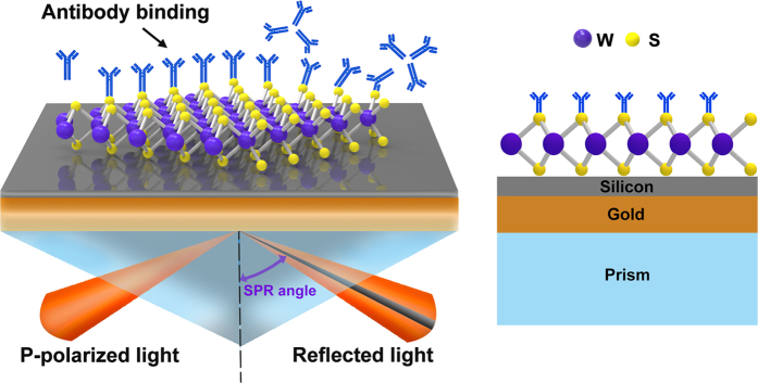
Based on these remarkable properties of silicon and group-IV semiconductor dichalcogenides, we propose a new configuration for sensitivity enhanced SPR biosensors based on silicon-MX2 heterostructures. As shown in Fig. 1, based on the Kretschmann attenuated total reflection (ATR) configurations, gold thin film is attached at the bottom of the SF10 prism followed by silicon nanosheet and 2D MX2. The 2D MX2 layers which are directly contacted with biomolecular analyte have dual effects: (i) as the signal-enhanced layer due to a high charge transfer efficiency from the MX2 surface to the Au surface42,43,44; (ii) as sensing platform to capture the biomolecules through the van der Waals interaction45,46.
Figure 1. Schematic diagram of silicon-WS2/ nanosheets-enhanced surface plasmon resonance biosensor.
Results and Discussion
In the ATR configuration, according to the principle of energy conversation the sum of the absorption A, reflectance R and transmittance T must be equal to 1 (i.e., A + R + T = 1) assuming no energy loss besides the materials absorption. Under the ATR condition, T is always equal to zero, hence the absorption of the system can be reduced to A = 1 − R. When the SPs were excited, the reflectance R gradually decreased until it reached a minimum. The minimum R was close to zero indicating that the incident energy was almost completely absorbed by the layered materials. Therefore, maximum incident light energy transfer to the evanescent wave is required in order to achieve the best SPR enhancement performance4,15,47,48.
Optimization of number of MX2 layers
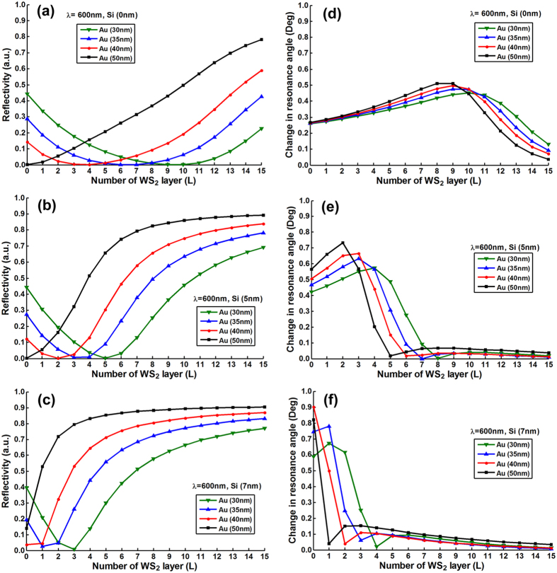
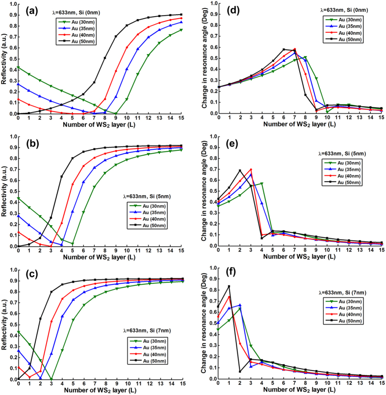
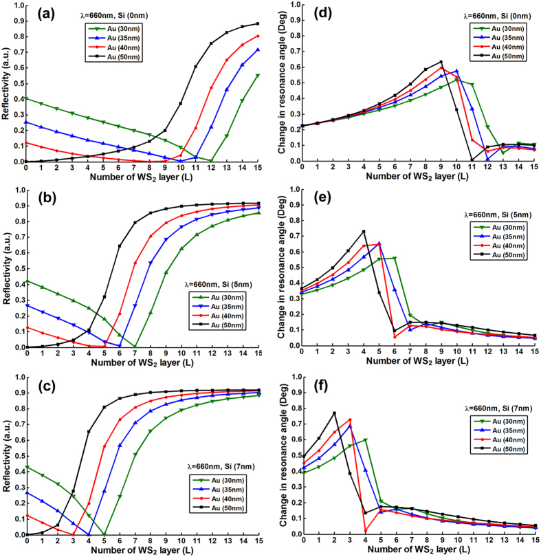
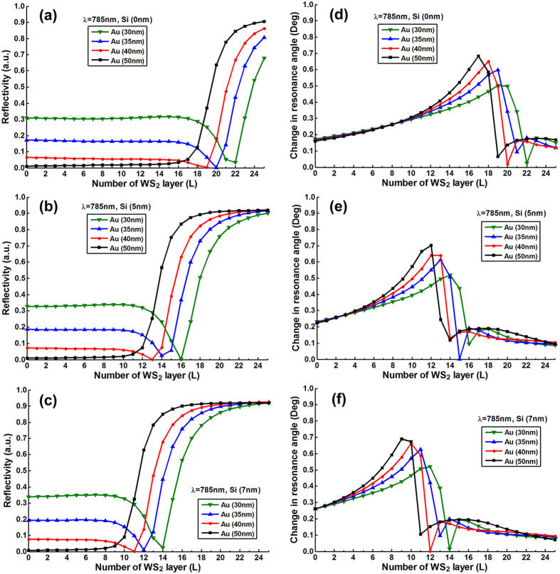
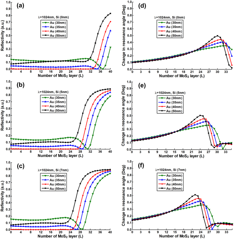
To optimize the number of MX2 layers, we plotted the resonance depths (i.e., the value of minimum reflectivity) change as a function of number of MX2 layers with various thickness of silicon nanosheet (i.e., 0 nm, 5 nm, 7 nm) and gold thin film (i.e., 30 nm, 35 nm, 40 nm, 50 nm). Figures 2a–c, 3a–c, 4a–c, 5a–c and 6a–c show the simulation results where different excitation wavelengths at 600 nm, 633 nm, 660 nm, 785 nm and 1024 nm were used. In general, two features for the SPR curves were observed: (i) When the silicon thickness was fixed and decreasing the gold thickness, the SPR dips redshifted with larger number of MX2 layers; similarly, when the thickness of gold thin film was fixed and decreasing the thickness of silicon, the reflectivity dips would also redshifted with the larger number of MX2 layers. This indicates that both silicon and MX2 layers can serve as absorption mediums and transfer energy to the gold thin film. (ii) It is worth noting that when the gold thickness was fixed at 50 nm, no MX2 is required to achieve the minimum reflectivity dip since 50 nm is the optimized thickness of gold thin film based on the conventional Kretschmann ATR configuration6. By analyzing the relationship between reflectivity and the number of MX2 layers, optimization of the number of MX2 layers was possible by selecting the specific number of layers that corresponded to the minimum resonance depths (i.e., the value of reflectivity that closest to zero). The detailed optimized number of MX2 layers with minimum reflectivity minR less than 0.03 were listed in Tables S1–S20 (Supplementary Information).
Figure 2.
The minimum reflectivity in SPR curve as a function of the number of WS2 layers at 600 nm excitation wavelength with various thickness of the gold thin film and silicon nanosheet (a) 0 nm (b) 5 nm (c) 7 nm; and the corresponding changes in the resonance angle for a fixed refractive index change in the biomolecular analyte (∆nbio = 0.005) as a function of the number of layers of WS2 at 600 nm excitation wavelength with various thickness of gold thin film and silicon nanosheet (d) 0 nm (e) 5 nm (f) 7 nm.
Figure 3.
The minimum reflectivity in SPR curve as a function of the number of WS2 layers at 633 nm excitation wavelength with various thickness of the gold thin film and silicon nanosheet (a) 0 nm (b) 5 nm (c) 7 nm; and the corresponding changes in the resonance angle for a fixed refractive index change in the biomolecular analyte (∆nbio = 0.005) as a function of the number of layers of WS2 at 633 nm excitation wavelength with various thickness of gold thin film and silicon nanosheet (d) 0 nm (e) 5 nm (f) 7 nm.
Figure 4.
The minimum reflectivity in SPR curve as a function of the number of WS2 layers at 660 nm excitation wavelength with various thickness of the gold thin film and silicon nanosheet (a) 0 nm (b) 5 nm (c) 7 nm; and the corresponding changes in the resonance angle for a fixed refractive index change in the biomolecular analyte (∆nbio = 0.005) as a function of the number of layers of WS2 at 660 nm excitation wavelength with various thickness of gold thin film and silicon nanosheet (d) 0 nm (e) 5 nm (f) 7 nm.
Figure 5.
The minimum reflectivity in SPR curve as a function of the number of WS2 layers at 785 nm excitation wavelength with various thickness of the gold thin film and silicon nanosheet (a) 0 nm (b) 5 nm (c) 7 nm; and the corresponding changes in the resonance angle for a fixed refractive index change in the biomolecular analyte (∆nbio = 0.005) as a function of the number of layers of WS2 at 785 nm excitation wavelength with various thickness of gold thin film and silicon nanosheet (d) 0 nm (e) 5 nm (f) 7 nm.
Figure 6.
The minimum reflectivity in SPR curve as a function of the number of WS2 layers at 1024 nm excitation wavelength with various thickness of the gold thin film and silicon nanosheet (a) 0 nm (b) 5 nm (c) 7 nm; and the corresponding changes in the resonance angle for a fixed refractive index change in the biomolecular analyte (∆nbio = 0.005) as a function of the number of layers of WS2 at 1024 nm excitation wavelength with various thickness of gold thin film and silicon nanosheet (d) 0 nm (e) 5 nm (f) 7 nm.
Thickness Optimization of gold and silicon layers
The optimized thickness of gold thin film and silicon nanosheet were obtained from the optimization of the sensitivity and FWHM. The SPR sensitivity serves as the key characteristic of SPR biosensor is defined in equation. (13) (See the Methods section). When the refractive index change of the biomolecules analyte layer (∆nbio = 0.005) was fixed, the sensitivity was governed by the change in resonance angle that acquired before and after the adsorption of biomolecules on the surface of the MX2 layers surface. Upon investigation of the variation of change in the resonance angle as a function of the number of MX2 layers as shown in Figs 2d–f to 6d–f three main features were observed: (i) As the number of MX2 layers increased, the change in resonance angle increased until it reached a maximum followed by a rapid decreasing to quasi-zero. (ii) When the excitation wavelength and gold thickness were fixed, the reduced thickness of silicon nanosheet caused the peak of the change in resonance angle to shift toward a larger number of MX2 layers; similarly, if the excitation wavelength and the silicon thickness were fixed, the decreased thickness of gold thin film also led to a peak shift to a larger number of MX2 layers. (iii) With fixed thickness of silicon and gold, the redshifted excitation wavelengths induced the peak shift of change in resonance angle towards the larger number of MX2 layers. Similar behaviors were also observed in Figs 2a–c to 6a–c (i.e., at longer excitation wavelengths, a larger number of MX2 was required to achieve the minimum reflectivity dip). This showed that the angular sensitivity decreases with longer excited wavelengths5, thereby higher refractive index materials are required to enhance the evanescent field.
With optimized number of MX2 layers, the angular sensitivity and FWHM of the four silicon-MX2 enhanced models were then analyzed under five different excitation wavelengths. When the excitation wavelength was set at 600 nm, the highest sensitivity 155.68 Deg/RIU was achieved with optimum parameters of 35 nm thickness gold film, 7 nm thickness silicon and monolayer WS2. The FWHM was 17.4644 Deg with a minimum reflectivity of 2.5592 × 10⁻² as shown in Table S1 (Supplementary Information). However, with the same thickness parameters and excitation wavelength, the highest sensitivity of silicon-MoSe2 enhanced model was only 104.56 Deg/RIU with a minimum reflectivity of 4.7627 × 10⁻³ as shown in Table S6 (Supplementary Information). This result can be explained by the different optical properties of WS2 and MoSe2. At 600 nm excitation wavelength, the real part of the dielectric constant of MoSe2 is 2 times as that of WS2, which indicates MoSe2 layers have higher energy absorption compared to WS2 layers. As a result, the minR of silicon-MoSe2 enhanced model is lower than that of silicon-WS2. However, the absorbed energy is not completely transferred to enhance the evanescent field due to the energy loss during the process. It is known that a dielectric material with a large real part and a small image part of the dielectric function have low energy loss, therefore the WS2 layers have much lower energy loss than that of MoSe2. Furthermore, the penetration depth of the evanescent field in the biomolecular analyte layer of the silicon-WS2 model is deeper than that of the silicon-MoSe2 model, since the real part of dielectric constant of WS2 is smaller than MoSe2 [6]. Consequently, the evanescent field of silicon-WS2 model is more sensitive than that of silicon-MoSe2 model to the refractive index change in biomolecular analyte. All these factors contributed to higher sensitivity in the silicon-WS2 enhanced scheme at 600 nm excitation wavelength. Similarly, the thickness combination for excitation wavelengths ranging from 633 nm to 1024 nm were also optimized (see Supplementary Information Tables S2–S20). Based on these results, we could conclude that although the MX2 layers with large real values of the dielectric constant contributed to the increased energy absorption, the intrinsic energy loss in these layers played a more significant role in the sensitivity of the multi-layered system.
Influence of excitation wavelength
In order to obtain the best SPR sensing performance, it is also important to achieve a relatively low FWHM as it promises more accurate determination of the angular modulation. The value of the FWHM is mainly depends on two factors: excitation wavelength and the number of MX2 layers. As reported previously, using longer excitation wavelength results in a narrower resonance curve6. As for the latter factor, our simulation results showed that large number of MX2 layers generated a higher value of FWHM since the additional MX2 layers resulted in higher electron energy loss and reduced the accuracy. To investigate the effect of the excitation wavelength, we summarized the optimized thickness combinations of gold thin film and silicon nanosheet for five different excitation wavelengths. As shown in Table 1, three features were observed: (i) By using 600 nm, 633 nm, 660 nm and 785 nm excitation wavelengths, the best performances were all achieved in the silicon-WS2 sensing model except for the 1024 nm excitation wavelength which was attained in the silicon-MoS2 scheme. This was due to the hybrid effects of the energy absorption and energy loss of MX2 layers at the different excitation wavelengths. (ii) For the visible range, the optimized thickness of silicon was 7 nm and the WS2 layers were required to be ultra-thin (i.e., 1–3 layers), the predicted sensitivity were all above 140 Deg/RIU. However, for the near-infrared range (i.e., 785 nm and 1024 nm), the optimized thickness of silicon and gold were determined to be 5 nm and 40 nm respectively, with the optimized number of MX2 layers being at least 13 and above. (iii) It is worth noting that as the excitation wavelength redshifted, the optimized sensitivity decreased gradually. The dielectric constant changes significantly with the increasing incident wavelengths. The real part of the dielectric constant is related to the reflectivity of the interface while the imaginary part is indicative of the energy absorption. Therefore, according to Table 1, as the wavelengths progressed into the near-infrared region, the hybrid effects resulted in higher attenuation of the evanescent field and thus lower SPR sensitivity was observed49.
Table 1. The optimized values of gold thin film, silicon nanosheet thickness and the number of MX2 layers with corresponding changes in resonance angle, sensitivities and FWHMs in SPR curves for 600 nm, 633 nm, 660 nm, 785 nm and 1024 nm excitation wavelengths.
| Excitation wavelength (nm) | Type of TMDC | Gold thickness (nm) | Silicon thickness (nm) | Number of WS2 layers (L) | Minimum Reflectivity | ΔθSPR(Deg) (Δnbio = 0.005) | Sensitivity (Deg/RIU) | FWHM (Deg) |
|---|---|---|---|---|---|---|---|---|
| 600 | WS2 | 35 | 7 | 1 | 2.5592 × 10⁻² | 0.7784 | 155.68 | 17.4644 |
| 633 | WS2 | 40 | 7 | 1 | 2.4099 × 10⁻² | 0.7394 | 147.88 | 16.2417 |
| 660 | WS2 | 40 | 7 | 3 | 3.3778 × 10⁻⁵ | 0.7282 | 145.64 | 16.8245 |
| 785 | WS2 | 40 | 5 | 13 | 2.5767 × 10⁻³ | 0.6395 | 127.90 | 15.5232 |
| 1024 | MoS2 | 40 | 5 | 26 | 1.6573 × 10⁻⁶ | 0.4499 | 89.98 | 17.5445 |
Optimized scheme for each of the Silicon-MX2 model
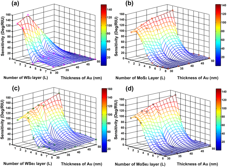
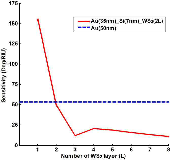
Finally, the parameters yielding the best performance for each of the silicon-WS2, silicon-WSe2, silicon-MoS2, silicon-MoSe2 enhanced SPR models are presented in Table 2. The optimized excitation wavelength and thickness of silicon nanosheet, gold thin film are the same for all the silicon-MX2 enhanced models except for the silicon-WS2 model. For the silicon-WS2 scheme, it possessed the highest sensitivity of 155.68 Deg/RIU with 35 nm thick gold and 7 nm silicon at the 600 nm wavelength. The 3D plots shown in Fig. 7a–d further validates the optimized parameters by depicting the sensitivity as a function of number of MX2 layers and gold thickness with the corresponding optimized silicon thickness and excitation wavelengths. From Fig. 7b–d, the highest value of sensitivity seemed to be attainable with 50 nm thick gold thin film and monolayer MX2. However, the minimum SPR reflectivity minR under these condition were greater than 0.03, leading to low energy-transfer efficiencies. In addition, the slopes of the sensitivity as a function of MX2 layers coated on 40 nm-thickness Au thin film were the sharpest among all the other Au thicknesses. Therefore, we concluded that the highest sensitivity of silicon-MoS2, silicon-MoSe2 and silicon-WSe2 models were obtained with 40 nm thick gold films. We also compared the sensitivity of our optimized configuration with the well-known conventional Kretschmann configuration (with 50 nm thickness gold thin film). As shown in Fig. 8, the sensitivity of our optimized silicon-WS2 enhanced configuration (155.68 Deg/RIU as shown in red solid line) is 3 times more sensitive than that of the Kretschmann design (53.40 Deg/RIU as shown in blue dashed line). For the Kretschmann configuration without any dielectric layers, the only absorbing medium in the system is the metal film; whereas in the silicon-WS2 enhanced structure the additional silicon nanosheet and MX2 layers can serve as the absorption medium as well. Moreover, the high refractive index of silicon nanosheet and the high real part of MX2 dielectric constant can enhance the evanescent field at the metal interface49. These double effects result in drastic sensitivity enhancement in the silicon-WS2 enhanced structure. In order to demonstrate the validity of our N-layer 2D models, we have experimentally tested the SPR sensing ability with 3-layer graphene-coated Au thin film. And both the angular and phase measurement results matched well with our theoretical analyses (see Supplementary Figs S1–S3).
Table 2. The optimized values of gold thin film, silicon nanosheet thickness and the number of MX2 layers with corresponding excitation wavelength, change in resonance angle, sensitivity and FWHM of the SPR curve for each silicon-MX2 nanosheet enhanced model.
| Excitation wavelength (nm) | Type of TMDC | Gold thickness (nm) | Silicon thickness (nm) | Number of WS2 layers (L) | Minimum Reflectivity | ΔθSPR (Deg) (Δnbio = 0.005) | Sensitivity (Deg/RIU) | FWHM (Deg) |
|---|---|---|---|---|---|---|---|---|
| 600 | WS2 | 35 | 7 | 1 | 2.5592 × 10⁻² | 0.7784 | 155.68 | 17.4644 |
| 633 | MoS2 | 40 | 7 | 1 | 1.1513 × 10⁻⁵ | 0.6586 | 131.70 | 17.5728 |
| 633 | WSe2 | 40 | 7 | 2 | 5.3807 × 10⁻³ | 0.7070 | 141.40 | 17.2340 |
| 633 | MoSe2 | 40 | 7 | 1 | 2.0438 × 10⁻³ | 0.6584 | 131.68 | 17.0915 |
Figure 7. The variation of the sensitivity as a function of gold thin film thickness and number of MX2 layers with 7 nm thick silicon nanosheet.
(a) The excitation wavelength is 600 nm in silicon-WS2 nanosheet enhanced model; (b) The excitation wavelength is 633 nm in silicon-MoS2 nanosheet enhanced model; (c) The excitation wavelength is 633 nm in silicon-WSe2 nanosheet enhanced model; (d) The excitation wavelength is 633 nm in silicon-MoSe2 nanosheet enhanced model.
Figure 8. Comparison of the SPR sensing performances between the optimized scheme of 35 nm thick gold thin film, 7 nm thick silicon nanosheet and monolayer WS2 (the red solid line) and the conventional Kretschmann configuration with 50 nm thick Au substrate (the blue dashed line).
Conclusion
In this study, we demonstrated a silicon nanosheet and 2D MX2 enhanced surface plasmon resonance biosensor. Based on the Kretschmann configuration, the system consists of SF10 triangular prism, gold thin film, silicon nanosheet and 2D MX2 film (MoS2/MoSe2/WS2/WSe2). To investigate the enhancement effect of each MX2 materials, we designed four enhanced models, namely, silicon-WS2, silicon-WSe2, silicon-MoS2 and silicon-MoSe2. Maxwell’s equations, Fresnel equations and transfer matrix method were used to analyze the change in resonance angle and the corresponding sensitivity for angular modulation. To study the influence of the excitation wavelengths to sensing performance, we studied five different excitation wavelengths, namely, 600 nm, 633 nm, 660 nm, 785 nm and 1024 nm. The results showed that the silicon nanosheet together with each of the four types of 2D MX2 layers could compensate the SPR effect of gold and significantly improve the sensitivity of the biosensor. However, excessive MX2 layers would result in increased energy loss and reduced the sensitivity. Therefore, in order to optimize the sensitivity, the thickness of gold film, silicon nanosheet and MX2 layers were investigated to minimize the reflectance and width of SPR curve to achieve a system with higher angular scanning accuracy. The combination of the optimized parameters for each excitation wavelength and each silicon-MX2 enhanced model were also presented with the highest SPR sensitivity of 155.68 Deg/RIU achieved using 35 nm thick gold film, 7 nm thick silicon nanosheet and a monolayer WS2 under the illumination of a 600 nm excitation wavelength source.
Methods
The wavelength-dependent refractive index for each layer
In this study, the theoretical analyses were performed with excitation light wavelengths in visible and near infrared ranges. Five wavelengths were chosen as 600 nm, 633 nm, 660 nm, 785 nm and 1024 nm respectively. The proposed configuration consists of 6 layer components, namley the SF10 prism, gold thin film, silicon nanosheet, 2D MX2 nanolayers (MoS2/WS2/MoSe2/WSe2), biomolecular analyte layer and sensing medium layer. The first component is the SF10 prism whose refractive index is given by50:
 |
where λ represents the wavelength of the light source in μm and Eq. (2) is valid for wavelengths from 0.38 μm to 2.5 μm. The refractive index of the gold thin film is determined using the Drude model by:
 |
where λp (1.6826 × 10⁻⁷ m) denotes the plasma wavelength and λc (8.9342 × 10⁻⁶ m) is the collision wavelength. λ in Eq. (3) represents the wavelength of the light source in μm, which is valid from 0.18 μm to 1.94 μm51,52,53. The thickness of the gold thin film was varied from 30 nm to 50 nm in this study. The refractive index of the silicon nanosheet is calculated by:
 |
where A = 3.44904, A1 = 2271.88813, A2 = 3.39538, t1 = 0.058304 and t2 = 0.30384, and λ is the wavelength in μm54. The thickness of the silicon sheet was varied from 0 nm to 7 nm. The fourth layer is the core functional layer −2D MX2 (MoS2/WS2/MoSe2/WSe2) whose refractive indexs and the monolayer thickness tMX2 are summarised in Table 3 55,56. The thickness of MX2 layers dMX2 is described by dMX2 = tMX2 × L, where L represents the number of MX2 layers. The fifth layer is the biomolecular analyte that dissolved in sensing medium. The change in refractive index of this layer can be induced by absorption of the biomolecules on the MX2 surface. Here the refractive index of this layer can be represented as nanalyte = 1.330 + ∆nbio, where ∆nbio indicates the change in refractive index of the biomolecular analyte. The thickness of this layer danalyte is fixed at 100 nm. The last layer is the sensing medium, the refractive index is defined as nsolvent = 1.330.
Table 3. The optical constants of 2D MoS2, MoSe2, WS2, and WSe2 with different excitation wavelengths from 600 nm to 1024 nm.
| TMDC | TMX2 (nm) | λ = 600 nm | λ = 633 nm | λ = 660 nm | λ = 785 nm | λ = 1024 nm |
|---|---|---|---|---|---|---|
| MoS2 | 0.65 | ɛ′ = 17.7967, | ɛ′ = 24.4368, | ɛ′ = 23.4129, | ɛ′ = 21.4675, | ɛ′ = 20.8372, |
| ɛ″ = 10.7801 | ɛ″ = 11.9121 | ɛ″ = 12.5610 | ɛ″ = 1.0781 | ɛ″ = 0.9662 | ||
| MoSe2 | 0.70 | ɛ′ = 21.3204, | ɛ′ = 20.3560, | ɛ′ = 19.3366, | ɛ′ = 17.7994, | ɛ′ = 14.9028, |
| ɛ″ = 10.9486 | ɛ″ = 9.3039 | ɛ″ = 8.4366 | ɛ″ = 7.0709 | ɛ″ = 2.7611, | ||
| WS2 | 0.80 | ɛ′ = 12.0258, | ɛ′ = 23.8511, | ɛ′ = 19.9701, | ɛ′ = 16.0968, | ɛ′ = 25.0445, |
| ɛ″ = 4.2578 | ɛ″ = 3.0578 | ɛ″ = 1.8420 | ɛ″ = 0.3203 | ɛ″ = 2.5676, | ||
| WSe2 | 0.70 | ɛ′ = 19.4125, | ɛ′ = 20.5156, | ɛ′ = 18.7344, | ɛ′ = 19.0563, | ɛ′ = 23.6474, |
| ɛ″ = 8.4135 | ɛ″ = 3.9423 | ɛ″ = 2.1955 | ɛ″ = 0.3205 | ɛ″ = 2.3801 |
The dielectric constant is described by
ε = ε′ + ε″i,
where the real part ε′
relates to the stored energy within the medium and the
imaginary part ε″ relates to
the dissipation of energy within the medium. (The complex
refractive index  is defined
as
 , where the real
part n indicates the phase velocity, while the
imaginary part κ known as the extinction
coefficient refers to the mass attenuation coefficient).
Reflection coefficient (r p ) and Reflectivity (R p )
In this study, the SPR biosensor model is based on the well-known Kretchmann’s attenuated total reflection (ATR) structure7. The incident light passes through the prism and is totally reflected at the base of the prism. Most of the light energy is absorbed by the metal and dielectric layers to generate the evanescent wave which propagates along the interface and penetrates into the sensing film. When the evanescent wave vector kx matches with the surface plasmon wave vector ksp, the resonance occurs as shown in Eq. (1). In order to analyse our N-layer structure model, the transfer matrix method (TMM) was employed. Each layer in our system was stacked horizontally in z-axis direction. All layers are defined by the parameters nk , εk and dk , which represent the refractive index, dielectric constant and thickness of the kth layer, respectively. θk denotes the incident angle of the kth layer and λ stands for the excitation wavelength.
To obtain the reflected intensity, Fresnel equations and relevant boundary conditions were introduced. In the calculations, the first boundary of the tangential fields was assumed as Z1 = 0, and the tangential fields at the last boundary ZN−1, there by giving rise to Eq. (5) as follows:
 |
where U1, UN−1 represent the tangential components of the first and the last layers in the electric fields, while V1, VN−1 denote the corresponding components in magnetic fields. M refers to the characteristic matrix of the N-layer model. For the p-polarized light, the characteristics matrix is given by:
 |
With
 |
Where
 |
 |
Thus, the four elements M11, M12, M21and M22 of the matrix M can be calculated. According to the Fresnel’s equations, the complex reflection coefficient rp of p-polarized incident electromagnetic field can be described by:
 |
where, q1and qN can be calculated from Eq. (8), which represent the relative components of the first layer and the Nth layer respectively. Therefore, the system reflectivity Rp for the p-polarized incident light can then be obtained by taking the square of the reflection coefficient rp, shown as follows:
 |
The angular sensitivity is defined as the ratio between the change of the resonance angle to the change of the analyte refractive index5 in Eq. (12).
 |
It can be simplified to
 |
The sensitivity describes the change in the optical signal (i.e., changes in the
resonance angle) corresponding to the minute changes in the refractive index of
the biomolecular analyte. The sensitivity depends on the evanescent field
strength which directly related to the absorbed light energy. Another key
parameter of interest is the width of the SPR curve, which related to the
accuracy of the sensing system. The width of SPR curve is determined by the
dielectric function of the metallic silicon-MX2 thin film. Generally,
a large value of  . sults in a narrow resonance
curve6. In this work, the full width at half maximum (FWHM)
is calculated to investigate the SPR curve width, as shown in Eq. (14),
 |
where θmin is the incident angle corresponding to the minimum reflected intensity, and θmax is the incident angle with the maximum reflected intensity base on the SPR curve.
Additional Information
How to cite this article: Ouyang, Q. et al. Sensitivity Enhancement of Transition Metal Dichalcogenides/Silicon Nanostructure-based Surface Plasmon Resonance Biosensor. Sci. Rep. 6, 28190; doi: 10.1038/srep28190 (2016).
Supplementary Material
Acknowledgments
This work was supported by the Singapore Ministry of Education (Grants Tier 2 MOE2010-T2-2-010 (M4020020.040 ARC2/11) and Tier 1 M4010360.040 RG29/10), NTU-NHG Innovation Collaboration Grant (No. M4061202.040), A*STAR Science and Engineering Research Council (No. M4070176.040), School of Electrical and Electronic Engineering at NTU, Guangdong Natural Science Foundation (2014A030312008) and Basic Research Foundation of Shenzhen (JCYJ20140418095735543).
Footnotes
Author Contributions Q.O., S.Z. and K.-T.Y. conceived the idea. Q.O., S.Z., L.J., L.H., G.X. and J.Q. designed and carried out the research. Q.O., S.Z. and K.-T.Y. co-wrote the manuscript. X.-Q.D., J.Q., S.H. and P.C. provided suggestions, and all authors commented on the manuscript.
References
- Zeng S., Baillargeat D., Ho H. P. & Yong K. T. Nanomaterials enhanced surface plasmon resonance for biological and chemical sensing applications. Chem. Soc. Rev. 43, 3426–3452 (2014). [DOI] [PubMed] [Google Scholar]
- Zeng S. et al. Graphene-gold metasurface architectures for ultrasensitive plasmonic biosensing. Adv. Mater. 27, 6163–6169 (2015). [DOI] [PubMed] [Google Scholar]
- Homola J. & Piliarik M. Surface Plasmon Resonance Based Sensors. Vol. 4 Ch. 2, 46–47 (Springer, 2006). [Google Scholar]
- Zeng S. et al. A review on functionalized gold nanoparticles for biosensing applications. Plasmonics. 6, 491–506 (2011). [Google Scholar]
- Shalabney A. & Abdulhalim I. Sensitivity-enhancement methods for surface plasmon sensors. Laser Photonics Rev. 5, 571–606 (2011). [Google Scholar]
- Kooyman R. P. H. Handbook of Surface Plasmon Resonance. (eds Schasfoort R. B. & Tudos A. J.) Ch. 2, 15–34 (Royal Society of Chemistry, 2008). [Google Scholar]
- Kretschmann E. & Raether H. Notizen. Radiative decay of non radiative surface plasmons excited by light. Z. Naturforsch. A. 23, 2135–2136 (1968). [Google Scholar]
- Otto A. Excitation of nonradiative surface plasma waves in silver by the method of frustrated total reflection. Z. Phys. 216, 398–410 (1968). [Google Scholar]
- Kabashin A. et al. Plasmonic nanorod metamaterials for biosensing. Nat. Mater. 8, 867–871 (2009). [DOI] [PubMed] [Google Scholar]
- Zhu M. et al. Low-temperature in situ growth of graphene on metallic substrates and its application in anticorrosion. ACS Appl. Mater. Interfaces. 8, 502–510 (2015). [DOI] [PubMed] [Google Scholar]
- Zhu M. et al. A wafer-scale graphene and ferroelectric multilayer for flexible and fast-switched modulation applications. Nanoscale. 7, 14730–14737 (2015). [DOI] [PubMed] [Google Scholar]
- Wu L., Chu H., Koh W. & Li E. Highly sensitive graphene biosensors based on surface plasmon resonance. Opt. Express. 18, 14395–14400 (2010). [DOI] [PubMed] [Google Scholar]
- Zeng S. et al. Graphene-MoS2 hybrid nanostructures enhanced surface plasmon resonance biosensors. Sens. Actuators B Chem. 207, 801–810 (2015). [Google Scholar]
- Mishra A. K., Mishra S. K. & Verma R. K. Graphene and beyond graphene MoS2: a new window in surface-plasmon-resonance-based fiber optic sensing. J. Phys. Chem. C. 120, 2893–2900 (2016). [Google Scholar]
- Verma R., Gupta B. D. & Jha R. Sensitivity enhancement of a surface plasmon resonance based biomolecules sensor using graphene and silicon layers. Sens. Actuators B Chem. 160, 623–631 (2011). [Google Scholar]
- Homola J. Surface plasmon resonance sensors for detection of chemical and biological species. Chem. Rev. 108, 462–493 (2008). [DOI] [PubMed] [Google Scholar]
- Zhang N. et al. Side-channel photonic crystal fiber for surface enhanced Raman scattering sensing. Sens. Actuators B Chem. 223, 195–201 (2016). [Google Scholar]
- Lu X. et al. Large-area synthesis of monolayer and few-layer MoSe2 films on SiO2 substrates. Nano Lett. 14, 2419–2425 (2014). [DOI] [PubMed] [Google Scholar]
- Ross J. S. et al. Electrical control of neutral and charged excitons in a monolayer semiconductor. Nat. Commun. 4, 1474 (2013). [DOI] [PubMed] [Google Scholar]
- Wang Q. H., Kalantar-Zadeh K., Kis A., Coleman J. N. & Strano M. S. Electronics and optoelectronics of two-dimensional transition metal dichalcogenides. Nat. Nanotechnol. 7, 699–712 (2012). [DOI] [PubMed] [Google Scholar]
- Kuc A., Zibouche N. & Heine T. Influence of quantum confinement on the electronic structure of the transition metal sulfide TS2. Phys. Rev. B. 83, 245213 (2011). [Google Scholar]
- Mak K. F., Lee C., Hone J., Shan J. & Heinz T. F. Atomically thin MoS2: a new direct-gap semiconductor. Phys. Rev. Lett. 105, 136805 (2010). [DOI] [PubMed] [Google Scholar]
- Radisavljevic B., Radenovic A., Brivio J., Giacometti V. & Kis A. Single-layer MoS2 transistors. Nat. Nanotechnol. 6, 147–150 (2011). [DOI] [PubMed] [Google Scholar]
- Tsai D. S. et al. Few-layer MoS2 with high broadband photogain and fast optical switching for use in harsh environments. Acs Nano. 7, 3905–3911 (2013). [DOI] [PubMed] [Google Scholar]
- Yu L. et al. Graphene/MoS2 hybrid technology for large-scale two-dimensional electronics. Nano Lett. 14, 3055–3063 (2014). [DOI] [PubMed] [Google Scholar]
- Roy K. et al. Graphene-MoS2 hybrid structures for multifunctional photoresponsive memory devices. Nat. Nanotechnol. 8, 826–830 (2013). [DOI] [PubMed] [Google Scholar]
- Britnell L. et al. Strong light-matter interactions in heterostructures of atomically thin films. Science. 340, 1311–1314 (2013). [DOI] [PubMed] [Google Scholar]
- Georgiou T. et al. Vertical field-effect transistor based on graphene-WS2 heterostructures for flexible and transparent electronics. Nat. Nanotechnol. 8, 100–103 (2013). [DOI] [PubMed] [Google Scholar]
- Cong C. et al. Synthesis and optical properties of large-area single-crystalline 2D semiconductor WS2 monolayer from chemical vapor deposition. Adv. Opt. Mater. 2, 131–136 (2014). [Google Scholar]
- Shi H., Pan H., Zhang Y. W. & Yakobson B. I. Quasiparticle band structures and optical properties of strained monolayer MoS2 and WS2. Phys. Rev. B. 87, 155304 (2013). [Google Scholar]
- Eda G. & Maier S. A. Two-dimensional crystals: managing light for optoelectronics. Acs Nano. 7, 5660–5665 (2013). [DOI] [PubMed] [Google Scholar]
- Sygletou M. et al. Laser induced nucleation of plasmonic nanoparticles on two-dimensional nanosheets for organic photovoltaics. J. Mater. Chem. A. 4, 1020–1027 (2016). [Google Scholar]
- Jones A. M. et al. Optical generation of excitonic valley coherence in monolayer WSe2. Nat. Nanotechnol. 8, 634–638 (2013). [DOI] [PubMed] [Google Scholar]
- Seyler K. L. et al. Electrical control of second-harmonic generation in a WSe2 monolayer transistor. Nat. Nanotechnol. 10, 407–411 (2015). [DOI] [PubMed] [Google Scholar]
- Koperski M. et al. Single photon emitters in exfoliated WSe2 structures. Nat. Nanotechnol. 10, 503–506 (2015). [DOI] [PubMed] [Google Scholar]
- Ross J. S. et al. Electrically tunable excitonic light-emitting diodes based on monolayer WSe2 pn junctions. Nat. Nanotechnol. 9, 268–272 (2014). [DOI] [PubMed] [Google Scholar]
- Tongay S. et al. Thermally driven crossover from indirect toward direct bandgap in 2D semiconductors: MoSe2 versus MoS2. Nano Lett. 12, 5576–5580 (2012). [DOI] [PubMed] [Google Scholar]
- Fan C. et al. Low temperature electrical and photo-responsive properties of MoSe2. Appl. Phys. Lett. 104, 202105 (2014). [Google Scholar]
- Huang C. et al. Lateral heterojunctions within monolayer MoSe2-WSe2 semiconductors. Nat. Mater. 13, 1096–1101 (2014). [DOI] [PubMed] [Google Scholar]
- Tonndorf P. et al. Photoluminescence emission and Raman response of monolayer MoS2, MoSe2, and WSe2. Opt. Express. 21, 4908–4916 (2013). [DOI] [PubMed] [Google Scholar]
- Lee S. H. et al. High-performance photocurrent generation from two-dimensional WS2 field-effect transistors. Appl. Phys. Lett. 104, 193113 (2014). [Google Scholar]
- Hoggard A. et al. Using the plasmon linewidth to calculate the time and efficiency of electron transfer between gold nanorods and graphene. Acs Nano. 7, 11209 (2013). [DOI] [PMC free article] [PubMed] [Google Scholar]
- Fang Z. et al. Gated tunability and hybridization of localized plasmons in nanostructured graphene. Acs Nano. 7, 2388 (2013). [DOI] [PubMed] [Google Scholar]
- Giovannetti G. et al. Doping graphene with metal contacts. Phys. Rev. Lett. 101, 026803 (2008). [DOI] [PubMed] [Google Scholar]
- Lee J. et al. Two-dimensional layered MoS2 biosensors enable highly sensitive detection of biomolecules. Sci. Rep. 4, (2014). [DOI] [PMC free article] [PubMed] [Google Scholar]
- Zhu C. et al. Single-layer MoS2-based nanoprobes for homogeneous detection of biomolecules. J. Am. Chem. Soc. 135, 5998–6001 (2013). [DOI] [PubMed] [Google Scholar]
- Homola J., Yee S. S. & Gauglitz G. Surface plasmon resonance sensors: review. Sens. Actuators B Chem. 54, 3–15 (1999). [Google Scholar]
- Lahav A., Auslender M. & Abdulhalim I. Sensitivity enhancement of guided-wave surface-plasmon resonance sensors. Opt. Lett. 33, 2539–2541 (2008). [DOI] [PubMed] [Google Scholar]
- Shalabney A. & Abdulhalim I. Electromagnetic fields distribution in multilayer thin film structures and the origin of sensitivity enhancement in surface plasmon resonance sensors. Sens. Actuators A Phys. 159, 24–32 (2010). [Google Scholar]
- Polyanskiy M. N. Refractive index database. Available at: http://refractiveindex.info.
- Johnson P. B. & Christy R. W. Optical constants of the noble metals. Phys. Rev. B. 6, 4370 (1972). [Google Scholar]
- Raether H. Surface Plasmons on Smooth Surfaces. Vol. 111, Ch. 2, 4–39 (Springer, 1988). [Google Scholar]
- Gupta B. & Sharma A. K. Sensitivity evaluation of a multi-layered surface plasmon resonance-based fiber optic sensor: a theoretical study. Sens. Actuators B Chem. 107, 40–46 (2005). [Google Scholar]
- Auslender M. & Hava S. Handbook of Optical Constants of Solids, Vol. 3 (eds Palik E. D.) Ch. 6, 155–186 (Elsevier, 1998). [Google Scholar]
- Li Y. et al. Measurement of the optical dielectric function of monolayer transition-metal dichalcogenides: MoS2, MoSe2, WS2, and WSe2. Phys. Rev. B. 90, 205422 (2014). [Google Scholar]
- Liu H. L. et al. Optical properties of monolayer transition metal dichalcogenides probed by spectroscopic ellipsometry. Appl. Phys. Lett. 105, 201905 (2014). [Google Scholar]
Associated Data
This section collects any data citations, data availability statements, or supplementary materials included in this article.


