Abstract
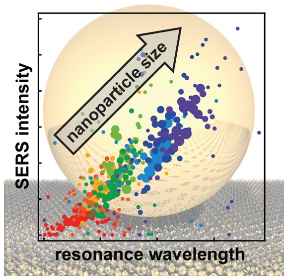
Coupling noble metal nanoparticles by a 1 nm gap to an underlying gold mirror confines light to extremely small volumes, useful for sensing on the nanoscale. Individually measuring 10 000 of such gold nanoparticles of increasing size dramatically shows the different scaling of their optical scattering (far-field) and surface-enhanced Raman emission (SERS, near-field). Linear red-shifts of the coupled plasmon modes are seen with increasing size, matching theory. The total SERS from the few hundred molecules under each nanoparticle dramatically increases with increasing size. This scaling shows that maximum SERS emission is always produced from the largest nanoparticles, irrespective of tuning to any plasmonic resonances. Changes of particle facet with nanoparticle size result in vastly weaker scaling of the near-field SERS, without much modifying the far-field, and allows simple approaches for optimizing practical sensing.
Surface-enhanced Raman spectroscopy (SERS) is an extremely powerful tool for sensing small molecular quantities at the nanoscale.1,2 For SERS, plasmonic nanostructures are used to focus light down to tiny volumes containing the analyte molecules. Countless different SERS substrates have been developed over the past decade, including bowtie antennas,3 nano rings,4 nanovoids,5 or nanoparticle aggregates.6−8 Nevertheless, a major problem is reproducibility: often the SERS signal differs among different nanostructures (or spots on the sample) due to variation in morphologies of nanostructures, and only very few sites exhibit the highest SERS enhancement. Hence it is advantageous to combine SERS with another faster spectroscopic technique to preselect promising nanostructures according to their plasmonic properties. A straightforward way is dark-field (DF) spectroscopy, which analyses light scattered from the nanostructures. It has the potential to be extremely fast9 and can be combined with imaging techniques to rapidly screen a large number of nanostructures at once. However, the key for such screening is in understanding the connection between the near-field (SERS enhancement) and far-field (scattering) properties of the nanostructures. Until now, this correlation has been hard to study as both the confined optical fields and the molecular orientations must be precisely constrained.
Each given gold nanostructure has a number of plasmonic resonances, and tuning the excitation laser to these wavelengths can greatly enhance the SERS intensity.10−12 However, the necessary broadband tunable lasers are still expensive and bulky and widely tuning the Raman filters is complicated. A second approach is instead to tune the plasmonic system to a given laser wavelength either by changing the composition of the nanostructure13 or by tuning the separation of two coupled systems.14,15 Here we instead simply scale the size of the nanoparticles, as this provides not only an easy method to tune the plasmonic resonance but also scales the strength of the resonant enhancement. Surprisingly this has not been carefully studied for single coupled nanoparticles before.
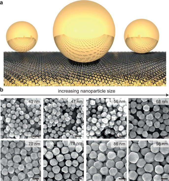
As a model system we use here the nanoparticle on mirror geometry (NPoM) consisting of individual gold nanoparticles placed on a continuous gold film separated by only a thin organic or semiconductor spacer layer (Figure 1a). The localized surface plasmons in the isolated gold nanoparticles couple to image charges induced in the gold film and thereby form a coupled plasmonic mode, which is tightly localized within the gap between nanoparticle and gold film. This geometry is easy to fabricate through self-assembly, allowing us to study thousands of identical plasmonic systems on a single substrate,16 and is highly reproducible. The large field enhancement enables spectroscopy of extremely small material quantities including monolayer materials of BN, MoS2, and CdSe,17,18 self-assembled monolayers,19 and down to single lipid molecules in lipid membranes.20 Here we use a biphenyl-4-thiol self-assembled monolayer as a spacer, which provides a reproducible and strong SERS signal when assembled inside the nanoparticle on mirror geometry. Without the nanoparticles, no Raman signal can be obtained from such layers.19
Figure 1.
(a) Schematic nanoparticle on mirror (NPoM) geometry. (b) Scanning electron microscopy (SEM) images of different-sized nanoparticle batches used. Average size was determined from 200 different nanoparticles (see SI). Scale bars are 70 nm.
The “spherical” gold nanoparticles, both homemade (see Methods) and purchased from different suppliers, have a variety of different crystal shapes with size distribution of widths between 3 to 7 nm (Figure 1b). The average nanoparticle size for each sample is determined by evaluating SEM images of 150 nanoparticles per batch (see Supporting Information (SI)). In order to fully account for this inhomogeneity we perform spectroscopy of over 10 000 individual particles in an automated unbiased way (Figure 2). Our custom-built Raman spectrometer uses a 632.8 nm HeNe laser coupled into a dark-field microscope, which is equipped with a computer controlled xyz-stage, and detected through laser-blocking filters by a monochromator and EMCCD camera. A second fiber-coupled spectrometer is used to record the dark-field spectra of each NPoM, with all the spectra background corrected and normalized to scattering off a broadband Lambertian scattering plate to thus compensate for chromatic aberrations in the optics and spectrometer. An imaging CCD camera is used to automatically find and center each particle, and subsequently dark-field (scattering) spectra at different focal heights (z) are recorded to compensate for chromatic aberration.16 Raman spectra are then recorded at the optimum height for 632.8 nm excitation as determined from the previously recorded z-stack. This is automatically repeated for over 1000 particles per sample (eight samples with different average particle sizes).
Figure 2.
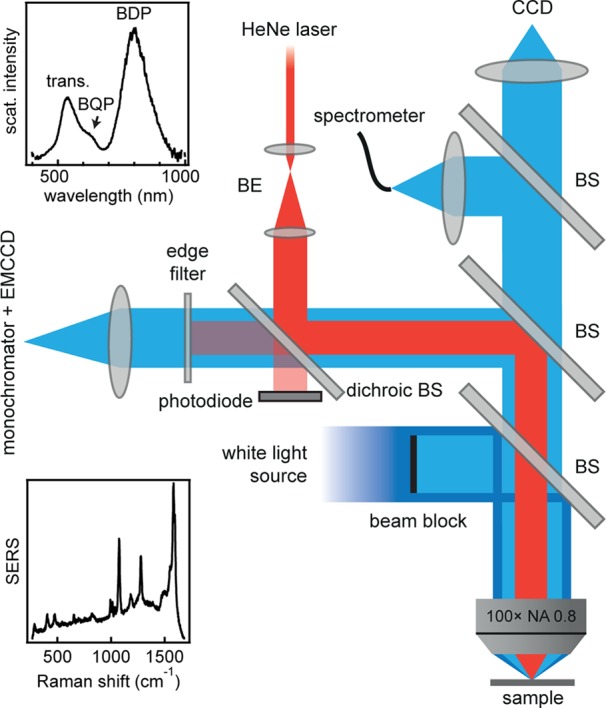
Schematic Raman/dark-field setup. Pump laser coupled into fully automated microscope with high NA (0.8) 100× objective; Raman emission is isolated with monochromator and EMCCD. Dark-field (DF) scattering spectra are collected by a second fiber-coupled spectrometer. Insets show representative scattering (top) and SERS (bottom) spectra from a single gold nanoparticle on mirror.
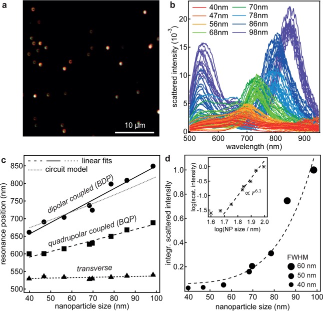
In DF images (Figure 3a), each nanoparticle-on-mirror appears as a green dot surrounded by a red ring. The green dot originates from the transverse (uncoupled) mode around 530 nm. The red ring stems from coupled modes, which are scattered toward angles of ∼60° with respect to the sample surface.21 The DF spectra reveal both the first and second order coupled modes: the fundamental bonding dipolar plasmon (BDP) is found at longer wavelengths, while the bonding quadrupolar plasmon (BQP) is located at shorter wavelengths between the transverse mode and the BDP. The BDP has the strongest nanoparticle size dependence (Figure 3c), shifting twice as much as the BQP, while the transverse mode barely shifts (27 times less shift). The average resonance positions with nanoparticle radius r [nm] shift near linearly as
 |
1 |
This matches well
our recent model for the
BDP mode based on lumped electrical components (gray dashed line, Figure 3c),22 with the intercepts given by  (for
plasma frequency λp, permittivity of surrounding
medium εm, and background
Au ε∞). Simultaneously, we
extract the scattering intensities and spectral widths (Figure 3d). The scattering intensity
of the BDP mode scales approximately as r6, which is expected from the classical model of polarizability.23 At the same time the mode broadens by approximately
50% (FWHM) as it is red-shifted.
Figure 3.
Plasmonic properties of nanoparticles-on-mirror of different sizes. (a) Typical darkfield image for 80 nm gold nanoparticles on a biphenyl-4-thiol self-assembled monolayer on an atomically smooth gold film. (b) Scattering spectra of different sized particles. (c) Evolution of the coupled modes (BDP and BQP) and the uncoupled (transverse) mode with increasing nanoparticle size, with prediction from LCR model (gray dotted).22 (d) Integrated scattered intensity of the BDP as a function of nanoparticle size. Marker size shows broadening of the BDP for larger nanoparticle sizes. Inset: log–log plot showing characteristic r6 dependence.
In order to correlate near- and far-field properties, we record both scattering and SERS spectra for each nanoparticle. The SERS spectra of biphenyl-4-thiol are highly reproducible among different nanoparticles and remain stable over time.19 As a proxy for the near-field enhancement we use the SERS intensity of the 1583 cm–1 vibration of the two phenyl rings (other modes show a similar behavior, see Figure S4). For the far-field properties we use the resonance wavelength of the BDP mode as it has the highest sensitivity to small size changes. Overall, larger Raman intensities are observed with increasing nanoparticle size (Figure 4a). Similar behavior has been found before for individual nanoparticles in solution.24,25 However, as recently reported, this behavior seems not to hold for gold nanorods.26 Doubling the NP size from 50 to 100 nm increases on average all Raman modes by a factor of 5.
Figure 4.
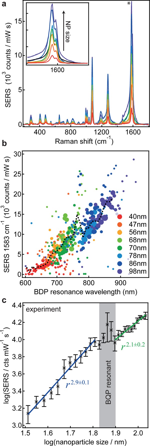
Correlation of SERS intensity and scattering resonance. (a) SERS spectra of a biphenyl-4-thiol self-assembled monolayer in the NPoM geometry with different nanoparticle sizes. the inset shows an enlarged view of the phenyl mode at 1583 cm–1. (b) SERS intensity as a function of the BDP resonance wavelength for over 10 000 single nanoparticles. For clarity, the single points are binned, and marker size gives the number of single spectra per bin. (c) Log–log plot of the average SERS intensity versus nanoparticle size.
To better characterize the inhomogeneous nanoparticle distributions, we correlate the SERS and dark-field spectra of over 10 000 individual nanoparticles. For clarity the data is shown in a binned form, sorted according to their BDP resonance wavelength (Figure 4b, with marker size corresponding to the number of particles in the respective bin). Although the SERS signal increases with increasing nanoparticle size (dashed line), this increase is not linear and can be subdivided into two regions with different scaling revealed on a log–log plot (Figure 4c). Both regions are separated by a peak where the BQP modes is resonant with the Raman laser.
For comparison, we have performed complementary FDTD simulations of spherical nanoparticles on mirror (separation = 1.3 nm, refractive index = 1.45). We use the product of the near-field intensity at the laser wavelength |E(λlaser)/E0|2 and at the Raman wavelength |E(λSERS)/E0|2 multiplied by the number of molecules n in the hotspot area as a gauge for the experimentally observed Raman signal. Despite showing two similar regions (see SI), the absolute values of the scaling are very different, with the experiments showing r2.9, while simulations show r7.6. This difference of theory and experiment can only be understood in terms of the nanoparticle shape: with increasing nanoparticle size the particles become increasingly nonspherical exhibiting increased facet sizes (Figure 1b and Figure 5). The majority of all nanoparticles are not spherical but show different crystal habits, with three examples for observed nanoparticle shapes shown in Figure 5a. Figure 5b shows the extracted facet diameter for different nanoparticle sizes. To estimate how faceting affects the SERS signal, we explore a simple model of how the smearing out of the trapped near-field over a larger area underneath the larger facets will reduce the maximum near-field strength. Assuming that the same near-field power is distributed over a larger area (given by the facet radius a), this thus decreases the nearfield intensity as a–2 (and therefore the SERS by a–4). To give a more rigorous picture including the appearance of new near-field modes18,27 and spectral shifts due to the faceting, we have performed FDTD simulations using circular facets with the characteristic facet diameters shown in Figure 5b for different nanoparticle sizes (keeping the nanoparticle volume constant; see SI). These simulations indeed show a very strong decrease of the Raman enhancement dependence (to r3.1) matching the experimentally observed scaling for smaller sizes. The increasingly dominant facets on larger nanoparticles spread out the confined optical field, thus reducing the maximum enhancements possible. Stable large spherical nanoparticles are thus desirable, but currently unattainable. For the largest sizes, our simulations predict a decrease of the SERS signal instead of the experimentally observed increase. We believe that this is due to our use of truncated spheres instead of the more complex true nanoparticle shapes, which are polyhedral. In spite of this, our model captures well the dramatic reduction in SERS compared to that expected from nanoparticle size scaling of the far-field scattering.
Figure 5.
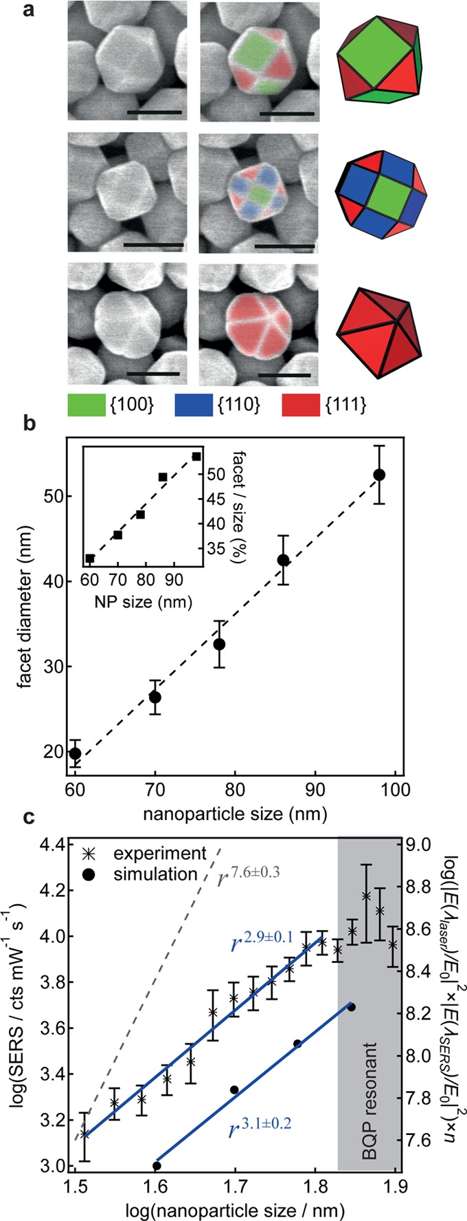
Gold nanoparticle faceting and impact on SERS enhancement. (a) SEM images and reconstructions of faceted nanoparticles with different shapes (from top to bottom): cuboctahedron, rhombicuboctahedron, and pentagonal bipyramid. The colors correspond to different lattice planes. (b) Nanoparticle facet size for different average nanoparticle sizes (measured from SEM images). (c) Experimental SERS vs nanoparticle size together with FDTD simulations assuming suitably faceted nanoparticles. The gray dashed line shows the scaling, which is predicted for spherical particles (see SI).
In conclusion, our results suggest that only changing the nanoparticle size in order to match one of the plasmonic resonances to either in- or out-coupling is not an efficient way to boost the SERS signal. Rather, using the largest possible nanoparticle size will produce the largest SERS signal. We observe that the increase of the SERS intensity (∝ r3) with nanoparticle size is lower than the increase in scattering (∝ r6). This is intrinsic to the nonresonant Raman spectroscopy and the increasingly nonspherical nanoparticle shapes. The shape alters both the near-field intensity and lateral distribution of the near-field, affecting the strength of the Raman signal. The fact that the near-field is much more strongly affected by the detailed nanoparticle morphology than the far-field response is a very general phenomenon in all tightly confined plasmonic cavities.
Methods
Sample Preparation. Atomically smooth gold substrates were prepared by evaporating 100 nm gold onto a clean silicon wafer (1 Å/s, Kurt J. Lesker ebeam evaporator). Subsequently, the wafer was heated to 60 °C, and small silicon pieces were glued to the freshly evaporated gold using Epo-Tek 377 epoxy glue. After curing the glue for 2 h at 150 °C and slowly cooling down, the silicon pieces can be peeled off revealing an atomically smooth clean gold surface. The wafer was stored, and gold pieces were peeled off on-demand.
Self-assembled monolayers of biphenyl-4-thiol (Sigma-Aldrich, 97%) were formed by submerging the substrates in a 1 mM solution in anhydrous ethanol (Sigma-Aldrich, < 0.003% H2O) for 22 h. The samples were thoroughly flushed with ethanol to remove any excess unbound thiol (confirmed by the absence of the characteristic –S–H stretch vibration in Raman) and blown dry.
Standard gold nanoparticles (Au NPs) in a citrate buffer were purchased from BBI solutions (80 nm, 100 nm) and CytoDiagnostics (70 nm, 90 nm). Additional samples (40–68 nm) were made in a three step seeded synthesis following the method of Ziegler et al.28 We modify the reported procedure by varying the amount of reductant and oxidant solution injected in the second seeded growth step. Au NPs with diameter of 40 ± 4 nm, 47 ± 6 nm, 56 ± 4 nm, and 68 ± 6 nm were produced by injecting 2.5 mL, 4.5 mL, 7.5 mL, and 15.5 mL of both the reductant (ascorbic acid/trisodium citrate) and oxidant (chloroauric acid) solution, respectively.
Gold nanoparticles were deposited onto the freshly prepared substrates by drop casting. As gold has an affinity toward the aromatic groups29,30 of the biphenyl-4-thiol self-assembled monolayer, nanoparticles bind rapidly to the substrate. The deposition time was adjusted to reach a uniform but sparse coverage. Excess nanoparticles were flushed off with deionized water and the sample was blown dry.
Simulation. Numerical simulations are carried out using Lumerical FDTD Solutions v8.12. The Au NP was modeled as a sphere or a truncated sphere (to model different facet size) of different diameters (40–120 nm) on top of an infinite dielectric sheet of refractive index 1.45 and thickness of 1.3 nm. Underneath this sheet, a thick gold layer was placed in order to replicate the experimental nanoparticle-on-mirror geometry. The dielectric function of gold was taken from Johnson and Christy.31 The nanoparticle was illuminated with a p-polarized plane wave (TFSF source) from an angle of incidence of θi= 55°. The inbuilt sweep parameter was used to sweep the incident wavelength from 500 to 900 nm. The scattered light of each wavelength was then collected within a cone of half angle θc= 55° based on the numerical aperture of the objective.
Acknowledgments
The authors thank Javier Aizpurua (CSIC – UPV/EHU/DIPC) for helpful discussions. We acknowledge financial support from EPSRC Grants EP/G060649/1, EP/K028510/1, EP/L027151/1, ERC Grant LINASS 320503. F.B. acknowledges support from the Winton Programme for the Physics of Sustainability. R.C. acknowledges support from the Dr. Manmohan Singh scholarship from St. John’s College.
Supporting Information Available
The Supporting Information is available free of charge on the ACS Publications website at DOI: 10.1021/acs.jpclett.6b00986. Source data can be found at DOI: 10.17863/CAM.54.
Nanoparticle size distribution, AFM characterization of the substrates, SEM and spectroscopy correlations, complementary FDTD simulations, example of resonance distribution curves, and correction factor for scattering at high angles (PDF)
Author Contributions
The experimental setup was built by F.B., B.d.N., and H.O., the automated particle tracking software is based on the original code by R.W.B. Experiments were planned and executed by F.B., B.d.N., and J.J.B. Nanoparticles were synthesized by A.S. AFM measurements were performed by J.M. and F.B. Electromagnetic simulations were performed by R.C. The data were analyzed by F.B., R.C., and J.J.B., and all authors contributed to the manuscript.
The authors declare no competing financial interest.
Supplementary Material
References
- Stiles P. L.; Dieringer J. A.; Shah N. C.; Van Duyne R. P. Surface-Enhanced Raman Spectroscopy. Annu. Rev. Anal. Chem. 2008, 1, 601–626. 10.1146/annurev.anchem.1.031207.112814. [DOI] [PubMed] [Google Scholar]
- Moskovits M. Surface-Enhanced Raman Spectroscopy: A Brief Retrospective. J. Raman Spectrosc. 2005, 36, 485–496. 10.1002/jrs.1362. [DOI] [Google Scholar]
- Hatab N. A.; Hsueh C.-H.; Gaddis A. L.; Retterer S. T.; Li J.-H.; Eres G.; Zhang Z.; Gu B. Free-Standing Optical Gold Bowtie Nanoantenna with Variable Gap Size for Enhanced Raman Spectroscopy. Nano Lett. 2010, 10, 4952–4955. 10.1021/nl102963g. [DOI] [PubMed] [Google Scholar]
- Ding T.; Herrmann L. O.; de Nijs B.; Benz F.; Baumberg J. J. Self-Aligned Colloidal Lithography for Controllable and Tuneable Plasmonic Nanogaps. Small 2015, 11, 2139–2143. 10.1002/smll.201402639. [DOI] [PMC free article] [PubMed] [Google Scholar]
- Sigle D. O.; Perkins E.; Baumberg J. J.; Mahajan S. Reproducible Deep-UV SERRS on Aluminum Nanovoids. J. Phys. Chem. Lett. 2013, 4, 1449–1452. 10.1021/jz4004813. [DOI] [PubMed] [Google Scholar]
- Kim T.; Lee K.; Gong M.; Joo S.-W. Control of Gold Nanoparticle Aggregates by Manipulation of Interparticle Interaction. Langmuir 2005, 21, 9524–9528. 10.1021/la0504560. [DOI] [PubMed] [Google Scholar]
- Taylor R. W.; Lee T.-C.; Scherman O. A.; Esteban R.; Aizpurua J.; Huang F. M.; Baumberg J. J.; Mahajan S. Precise Subnanometer Plasmonic Junctions for SERS within Gold Nanoparticle Assemblies Using Cucurbit[n]uril “Glue.. ACS Nano 2011, 5, 3878–3887. 10.1021/nn200250v. [DOI] [PubMed] [Google Scholar]
- Patra P. P.; Chikkaraddy R.; Tripathi R. P. N.; Dasgupta A.; Kumar G. V. P. Plasmofluidic Single-Molecule Surface-Enhanced Raman Scattering from Dynamic Assembly of Plasmonic Nanoparticles. Nat. Commun. 2014, 5, 4357. 10.1038/ncomms5357. [DOI] [PubMed] [Google Scholar]
- Herrmann L. O.; Baumberg J. J. Watching Single Nanoparticles Grow in Real Time through Supercontinuum Spectroscopy. Small 2013, 9, 3743–3747. 10.1002/smll.201300958. [DOI] [PubMed] [Google Scholar]
- McFarland A. D.; Young M. A.; Dieringer J. A.; Van Duyne R. P. Wavelength-Scanned Surface-Enhanced Raman Excitation Spectroscopy. J. Phys. Chem. B 2005, 109, 11279–11285. 10.1021/jp050508u. [DOI] [PubMed] [Google Scholar]
- Zhu W.; Crozier K. B. Quantum Mechanical Limit to Plasmonic Enhancement as Observed by Surface-Enhanced Raman Scattering. Nat. Commun. 2014, 5, 5228. 10.1038/ncomms6228. [DOI] [PubMed] [Google Scholar]
- Lombardi A.; Demetriadou A.; Weller L.; Andrae P.; Benz F.; Chikkaraddy R.; Aizpurua J.; Baumberg J. J. Anomalous Spectral Shift of near- and Far-Field Plasmonic Resonances in Nano-Gaps. ACS Photonics 2016, 3, 471–477. 10.1021/acsphotonics.5b00707. [DOI] [PMC free article] [PubMed] [Google Scholar]
- Jackson J. B.; Halas N. J. Surface-Enhanced Raman Scattering on Tunable Plasmonic Nanoparticle Substrates. Proc. Natl. Acad. Sci. U. S. A. 2004, 101, 17930–17935. 10.1073/pnas.0408319102. [DOI] [PMC free article] [PubMed] [Google Scholar]
- Kahraman M.; Daggumati P.; Kurtulus O.; Seker E.; Wachsmann-Hogiu S. Fabrication and Characterization of Flexible and Tunable Plasmonic Nanostructures. Sci. Rep. 2013, 3, 3396. 10.1038/srep03396. [DOI] [PMC free article] [PubMed] [Google Scholar]
- Alexander K. D.; Skinner K.; Zhang S.; Wei H.; Lopez R. Tunable SERS in Gold Nanorod Dimers through Strain Control on an Elastomeric Substrate. Nano Lett. 2010, 10, 4488–4493. 10.1021/nl1023172. [DOI] [PubMed] [Google Scholar]
- de Nijs B.; Bowman R. W.; Herrmann L. O.; Benz F.; Barrow S. J.; Mertens J.; Sigle D. O.; Chikkaraddy R.; Eiden A.; Ferrari A.; et al. Unfolding the Contents of Sub-Nm Plasmonic Gaps Using Normalising Plasmon Resonance Spectroscopy. Faraday Discuss. 2015, 178, 185–193. 10.1039/C4FD00195H. [DOI] [PubMed] [Google Scholar]
- Sigle D. O.; Hugall J. T.; Ithurria S.; Dubertret B.; Baumberg J. J. Probing Confined Phonon Modes in Individual CdSe Nanoplatelets Using Surface-Enhanced Raman Scattering. Phys. Rev. Lett. 2014, 113, 87402. 10.1103/PhysRevLett.113.087402. [DOI] [PubMed] [Google Scholar]
- Sigle D. O.; Mertens J.; Herrmann L. O.; Bowman R. W.; Ithurria S.; Dubertret B.; Shi Y.; Yang H. Y.; Tserkezis C.; Aizpurua J.; et al. Monitoring Morphological Changes in 2D Monolayer Semiconductors Using Atom-Thick Plasmonic Nanocavities. ACS Nano 2015, 9, 825–830. 10.1021/nn5064198. [DOI] [PMC free article] [PubMed] [Google Scholar]
- Benz F.; Tserkezis C.; Herrmann L. O.; de Nijs B.; Sanders A.; Sigle D. O.; Pukenas L.; Evans S. D.; Aizpurua J.; Baumberg J. J. Nanooptics of Molecular-Shunted Plasmonic Nanojunctions. Nano Lett. 2015, 15, 669–674. 10.1021/nl5041786. [DOI] [PMC free article] [PubMed] [Google Scholar]
- Taylor R. W.; Benz F.; Sigle D. O.; Bowman R. W.; Bao P.; Roth J.; Heath G. R.; Evans S. D.; Baumberg J. J. Watching Individual Molecules Flex within Lipid Membranes Using SERS. Sci. Rep. 2014, 4, 5940. 10.1038/srep05940. [DOI] [PMC free article] [PubMed] [Google Scholar]
- Yamamoto N.; Ohtani S.; García de Abajo F. J. Gap and Mie Plasmons in Individual Silver Nanospheres near a Silver Surface. Nano Lett. 2011, 11, 91–95. 10.1021/nl102862x. [DOI] [PubMed] [Google Scholar]
- Benz F.; de Nijs B.; Tserkezis C.; Chikkaraddy R.; Sigle D. O.; Pukenas L.; Evans S. D.; Aizpurua J.; Baumberg J. J. Generalized Circuit Model for Coupled Plasmonic Systems. Opt. Express 2015, 23, 33255–33269. 10.1364/OE.23.033255. [DOI] [PubMed] [Google Scholar]
- Pelton M.; Bryant G. W.. Introduction to Metal-Nanoparticle Plasmonics; Wiley: Hoboken, NJ, 2013. [Google Scholar]
- Njoki P. N.; Lim I.-I. S.; Mott D.; Park H.-Y.; Khan B.; Mishra S.; Sujakumar R.; Luo J.; Zhong C.-J. Size Correlation of Optical and Spectroscopic Properties for Gold Nanoparticles. J. Phys. Chem. C 2007, 111, 14664–14669. 10.1021/jp074902z. [DOI] [Google Scholar]
- Hong S.; Li X. Optimal Size of Gold Nanoparticles for Surface-Enhanced Raman Spectroscopy under Different Conditions, Optimal Size of Gold Nanoparticles for Surface-Enhanced Raman Spectroscopy under Different Conditions. J. Nanomater. 2013, 2013, 790323. 10.1155/2013/790323. [DOI] [Google Scholar]
- Lin K.-Q.; Yi J.; Hu S.; Liu B.-J.; Liu J.-Y.; Wang X.; Ren B. Size Effect on SERS of Gold Nanorods Demonstrated via Single Nanoparticle Spectroscopy. J. Phys. Chem. C 2016, 10.1021/acs.jpcc.6b02098. [DOI] [Google Scholar]
- Tserkezis C.; Esteban R.; Sigle D. O.; Mertens J.; Herrmann L. O.; Baumberg J. J.; Aizpurua J. Hybridization of Plasmonic Antenna and Cavity Modes: Extreme Optics of Nanoparticle-on-Mirror Nanogaps. Phys. Rev. A: At., Mol., Opt. Phys. 2015, 92, 53811. 10.1103/PhysRevA.92.053811. [DOI] [Google Scholar]
- Ziegler C.; Eychmüller A. Seeded Growth Synthesis of Uniform Gold Nanoparticles with Diameters of 15–300 nm. J. Phys. Chem. C 2011, 115, 4502–4506. 10.1021/jp1106982. [DOI] [Google Scholar]
- Miessler G. L.; Fischer P. J.; Tarr D. A.. Inorganic Chemistry; Pearson: Boston, MA, 2014. [Google Scholar]
- Netzer F. P.; Ramsey M. G. Structure and Orientation of Organic Molecules on Metal Surfaces. Crit. Rev. Solid State Mater. Sci. 1992, 17, 397–475. 10.1080/10408439208243753. [DOI] [Google Scholar]
- Johnson P. B.; Christy R. W. Optical Constants of the Noble Metals. Phys. Rev. B 1972, 6, 4370–4379. 10.1103/PhysRevB.6.4370. [DOI] [Google Scholar]
Associated Data
This section collects any data citations, data availability statements, or supplementary materials included in this article.


