Significance
Extreme magnetoresistance (XMR) has been recently discovered in a number of seemingly unrelated materials with diverse crystalline and electronic structures. In this work, we use lanthanum monopnictides, LaBi and LaSb, as simple platforms to reveal a common triangular Temperature–field phase diagram for XMR. Further, we show that, in the electronic structure of both materials, lanthanum d orbitals mix with the pnictogen p orbitals. Remarkably, we find that both the triangular phase diagram and the orbital texture exist in all families of semimetals with XMR. These results show that XMR is a ubiquitous phenomenon with a universal phase diagram that goes beyond certain material specifications; it is not a rare commodity of topological materials or noncentrosymmetric structures.
Keywords: extreme magnetoresistance, topological semimetal, orbital texture
Abstract
The recent discovery of extreme magnetoresistance (XMR) in LaSb introduced lanthanum monopnictides as a new platform to study this effect in the absence of broken inversion symmetry or protected linear band crossing. In this work, we report XMR in LaBi. Through a comparative study of magnetotransport effects in LaBi and LaSb, we construct a temperature−field phase diagram with triangular shape that illustrates how a magnetic field tunes the electronic behavior in these materials. We show that the triangular phase diagram can be generalized to other topological semimetals with different crystal structures and different chemical compositions. By comparing our experimental results to band structure calculations, we suggest that XMR in LaBi and LaSb originates from a combination of compensated electron−hole pockets and a particular orbital texture on the electron pocket. Such orbital texture is likely to be a generic feature of various topological semimetals, giving rise to their small residual resistivity at zero field and subject to strong scattering induced by a magnetic field.
Materials with large magnetoresistance (MR) have applications in electronics as magnetic memories (1, 2), in spintronics as magnetic valves (3), and in industry as magnetic sensors or magnetic switches (4, 5). Recent reports of extreme magnetoresistance (XMR) in several nonmagnetic semimetals have attracted attention due to its distinction from giant and collosal MR in magnetic semiconductors (2, 6). XMR is observed in Dirac semimetals such as Na3Bi or Cd3As2 (7, 8), Weyl semimetals such as NbP, NbAs, or TaAs (9–11), and layered semimetals such as WTe2, NbSb2, or PtSn4 (12–16). The recent discovery of XMR in LaSb that does not belong to any of these categories shows that XMR is a ubiquitous phenomenon observed in seemingly unrelated materials (17). It also clearly underlines that the mechanism for XMR is not understood. The present article is a first attempt to unify the phenomenology of XMR in seemingly unrelated materials, to provide a common phase diagram for XMR, and to elucidate its underlying mechanism. We hope that this will enable theorists to develop a model capable of describing the underlying physics, once all of the salient experimental features are captured.
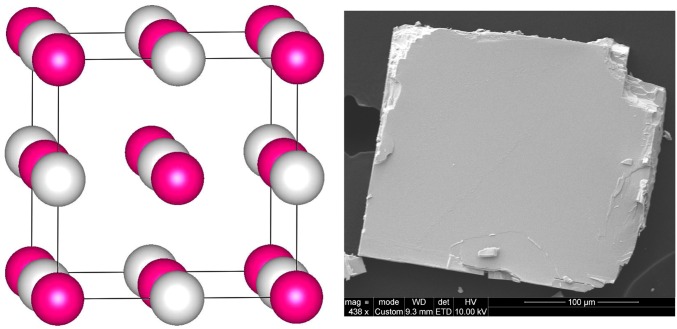
We report the discovery of XMR in LaBi with similar crystal structure and chemical composition to LaSb. Fig. 1 shows the simple rock salt structure of lanthanum monopnictides. Through a comparative study of longitudinal and transverse magnetotransport in LaSb and LaBi, we construct a characteristic triangular T-H phase diagram for XMR in lanthanum monopnictides. Our band structure calculations, quantum oscillations, and Hall Effect measurements suggest that XMR is rooted in a combination of compensated electron−hole pockets and a mixed orbital texture within the electron pockets. The orbital texture is a result of lanthanum d states crossing the pnictogen p states. Spin−orbit coupling then opens a small gap at the point of crossing to form the electron pocket with mixed d−p orbital texture. A recent theoretical work pointed to the topological nature of lanthanum monopnictides that results from this crossing (18). Here, we show that a similar orbital texture exists in other topological semimetals and so does the triangular T-H phase diagram. The finding of a universal phase diagram across materials with diverse structures and chemical compositions implies that XMR is a ubiquitous phenomenon and expected to be found in many more compounds.
Fig. 1.
(Left) NaCl-type crystal structure of LaSb/LaBi with space group . Gray spheres represent La, and pink spheres represent Sb/Bi. (Right) Scanning Electron Microscopy image of LaBi single crystal showing cubic symmetry and the cleaved [100] surface. X-ray refinements are presented in Supporting Information.
Results
Temperature Dependence of Resistivity.
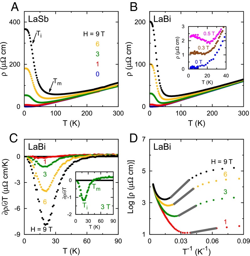
Fig. 2 A and B shows the temperature dependence of resistivity in LaSb and LaBi. At T (black curves), with decreasing temperature, resistivity decreases initially until a minimum at , then increases until an inflection at where it gradually saturates to a plateau. Fig. 2B, Inset shows that the resistivity upturn is absent at zero field. It is switched on with a small magnetic field T and becomes more prominent as the field increases, promising applications such as low-temperature magnetic switches and sensors.
Fig. 2.
(A) Resistivity as a function of temperature in LaSb at several magnetic fields as indicated on the figure. Temperature of resistivity minimum and inflection are marked on the black curve at T. (B) The in LaBi at the same fields as in LaSb. Inset shows at low T and low H with the onset of resistivity upturn at T. (C) The as a function of temperature in several fields as indicated on the figure for LaBi. Inset shows the sign change temperature and the peak temperature for the green curve at T. (D) Arrhenius plot of versus used to extract the activation energy at several fields. The gray part of the traces indicates the temperature range used to extract the activation energy.
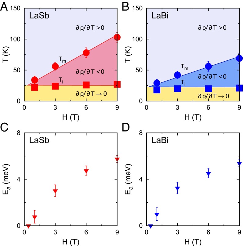
Fig. 2C is a plot of versus T for LaBi that marks as the temperature where changes sign and as the temperature where shows a peak. With increasing field, increases but remains unchanged. Fig. 2D is an Arrhenius plot of versus for LaBi showing that, in the narrow region between and , resistivity fits to where is the activation energy and is the Boltzmann constant. is plotted as a function of field for LaSb and LaBi in Fig. 3 C and D. At first, such analysis may suggest a metal−insulator transition (MIT) at , but, as we explain later, this is certainly not the case.
Fig. 3.
(A) (circles) and (squares) plotted as a function of H in LaSb. For fields below T, and are the same within our experimental precision, but they diverge for fields larger than . Although is almost field-independent, increases linearly over the measured field range. This gives rise to a triangular shape area in the H-T phase diagram where XMR occurs. The silver region above the circles is where behaves like a conventional metal. The gold region below the squares is where plateaus. (B) Similar triangular phase diagram for LaBi. (C) Activation energy extracted from the Arrhenius analysis and plotted as a function of magnetic field for LaSb. Error bars represent maximum change of by changing the fitting range. (D) plotted as a function of field for LaBi.
Phase Diagram.
By plotting and as a function of magnetic field, we construct the temperature−field phase diagram of XMR in LaSb and LaBi (Fig. 3 A and B). In both systems, increases with increasing field whereas stays unchanged. The shaded triangle between and marks the region of MR where (Fig. 2C, Inset). The silver area above the triangle ( ) in Fig. 3 A and B is the region of metallic conduction where with negligible MR which is quadratic in field. The gold area below the triangle ( ) is the plateau region where . Toward the end of the paper, we will show that the triangular phase diagram is universal to all semimetals with XMR (see Fig. 9).
Fig. 9.
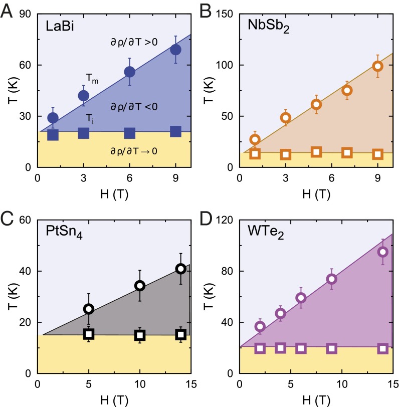
(A) Triangular T-H phase diagram of LaBi, same as in Fig. 3A, compared with three different topological semimetals in the subsequent panels. (B) Triangular T-H phase diagram in NbSb2 constructed with the data from ref. 15. (circles) and (squares) are the temperatures of resistivity minimum and inflection. Open symbols are used for all of the adapted data. (C) Triangular T-H phase diagram in PtSn4 constructed with the data from ref. 16. (D) Triangular T-H phase diagram in WTe2 constructed with the data from ref. 12. Aside from variations in the absolute values of and that depend on sample purity and XMR magnitude, these different topological semimetals share the same phase diagram.
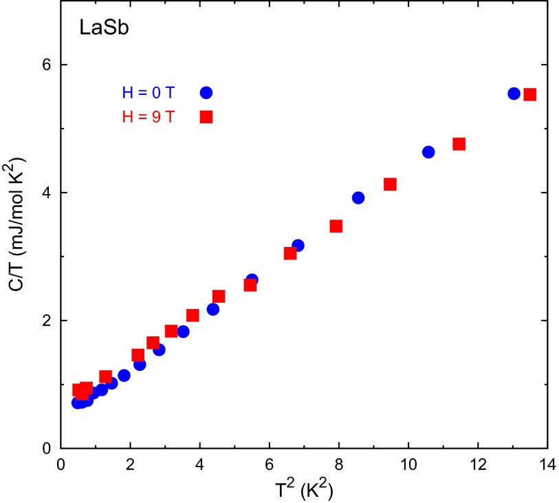
Fig. 3 shows that LaSb and LaBi have comparable but different . If an MIT was responsible for the resistivity upturn, then the smaller in LaBi should have translated to a smaller . Additional evidence against an MIT comes from a comparison of the electronic specific heat in and in an applied field of T (Fig. S1). Recent work on another XMR material, WTe2, has also ruled out field-induced MIT at through a scaling analysis and the use of Kohler’s rule (19, 20). In the absence of an MIT, the resistivity upturn at must result from a strong field-induced scattering. We will elaborate on such scattering process after discussing the band structure of LaBi and LaSb.
Fig. S1.
Heat capacity of LaSb measured down to 0.5 K in a Helium 3 fridge. is plotted as a function of .
Field Dependence of Resistivity and XMR.
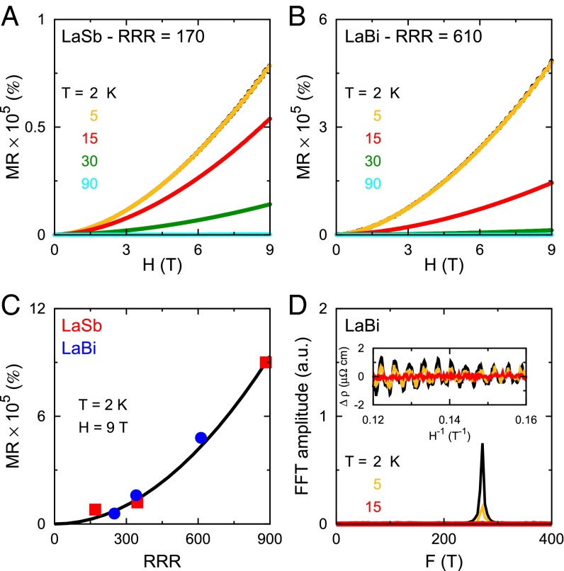
Fig. 4 A and B shows MR = , as a function of magnetic field from T to 9 T at several temperatures. The black and the yellow curves at T = 2 K and 5 K superimpose because both curves are in the plateau region where MR reaches its extreme limit in excess of . Comparing Fig. 4 A and B with the phase diagram Fig. 3 A and B shows that MR is small in the conventional metallic region at , it starts to increase in the region of field-induced scattering at , and it reaches the extreme limit in the plateau region at . Ref. 17 shows that the magnitude of XMR is sensitive to the residual resistivity ratio (RRR), i.e., to the sample quality. We quote RRR values for the LaSb and the LaBi samples in Fig. 4 A and B to prevent the reader from taking away the wrong conclusion that the XMR in LaSb is smaller than in LaBi. Fig. 4C is a plot of MR as a function of RRR for several LaSb and LaBi specimens with different RRR values. MR in both materials follows the same quadratic dependence on RRR, showing a comparable XMR in both compounds given comparable sample quality. A similar quadratic dependence of XMR on RRR is reported in the flux-grown WTe2 samples (13).
Fig. 4.
(A) MR as a function of field in LaSb sample with RRR = 170 at several temperatures indicated on the figure. SdH oscillations appear at higher fields. (B) MR as a function of field for LaBi sample with RRR = 610. (C) MR at K and T plotted as a function of RRR for several LaSb (square) and LaBi (circle) samples. The solid black line is a quadratic fit that correlates RRR and XMR: Samples with larger RRR (smaller ) have larger XMR. (D) Inset shows the oscillatory part of resistivity, , at several temperatures for LaBi. FFT of these data are plotted as a function of frequency with a peak at T.
The ripples in the resistivity at higher fields in Fig. 4 A and B are Shubnikov−de Haas (SdH) oscillations. The purely oscillatory part of resistivity is obtained by subtracting a smooth background from in the range from −9 T. is periodic in as seen in Fig. 4D, Inset. Fast Fourier Transform (FFT) of these data gives a peak at T in Fig. 4D for LaBi. Similar analysis gives T for LaSb (17). The principal frequencies for LaSb and LaBi do not match the known frequencies of tin and indium, ruling out flux inclusion (21, 22).
Angle Dependence of XMR and SdH Oscillations.
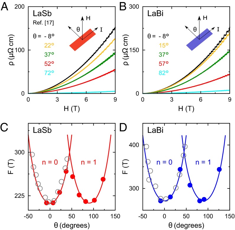
Fig. 5 A and B shows the angle dependence of XMR in LaSb and LaBi. The direction of magnetic field H and electrical current I with respect to [100] crystal plane is shown schematically. XMR is maximum when and minimum when . It remains positive at all angles. Fig. 5 C and D shows that the principal frequency in LaSb and LaBi has the following angle dependence:
| [1] |
where n is an integer, θ is the angle, and is the principal frequency at . Such angle dependence describes either a strictly 2D Fermi surface such as TI surface modes (25–27) or a quasi-2D bulk state such as the prolate ellipsoidal geometry of the electron pocket in lanthanum monopnictides (Fig. 6 C and D). Fig. 5C shows perfect agreement between our data and prior studies of magnetic oscillations (gray symbols) (23, 24, 28, 29).
Fig. 5.
(A) Resistivity as a function of magnetic field in LaSb at five representative angles as indicated. MR decreases with increasing θ. LaSb data are adapted from ref. 17. (B) The in LaBi at five representative angles as indicated. MR stays positive at all angles in both systems. (C) SdH frequency as a function of angle in LaSb. Open gray circles are de Haas-van Alphen (dHvA) data from ref. 23. Solid lines are fits to Eq. 1 with T. (D) SdH oscillation frequency as a function of angle in LaBi. Solid lines are fits to Eq. 1 with T. Open gray symbols are dHvA data from ref. 24.
Fig. 6.
(A) Band structure of LaSb with two hole pockets that cross near and one electron pocket that crosses near X. The crossing between La d states (thin bands) and Sb p states (thick bands) near X gives a d−p texture to the electron pocket. Inset shows a small gap at this crossing due to spin−orbit coupling. (B) Band structure of LaBi with the same d−p crossing between La thin bands and Bi thick bands near X. Inset shows a small gap at this crossing due to spin-orbit coupling. (C) Fermi surfaces of LaSb in the first Brillouin zone with the central hole pockets and the peripheral electron pockets (prolate ellipsoids). SdH frequencies in Fig. 5 correspond to ellipsoidal electron pockets. (D) Similar Fermi surfaces of LaBi.
Band Structure and the Orbital Texture.
Fig. 6 A and B shows the results of our band structure calculations on LaSb and LaBi with the WIEN2k code using the full relativistic treatment of spin−orbit coupling (30). In both systems, two hole bands at the point and one electron band near the X point cross the Fermi level . Fig. 6 C and D visualize the corresponding Fermi surfaces with the two hole surfaces at the center of the Brillouin zone and the ellipsoidal electron pockets crossing the faces. Prior studies of quantum oscillations in the magnetic and acoustic channels have mapped these hole and electron Fermi surfaces in both materials in detail (23, 24, 28, 29). The principal SdH frequencies that we observe in LaSb ( T) and LaBi ( T) match the cross-sectional area of the electron pocket at the X point.
We plot Antimony p states as thick bands and lanthanum d states as thin bands in Fig. 6 A and B. Notice the crossing between these bands near the X point. Spin−orbit coupling opens a small gap as shown in Fig. 6 A and B, Insets to form the electron pocket. The orbital character of momentum states changes from d to p as they wind around this electron pocket. Such winding of the orbital quantum number around the electron pocket could translate to a pseudospin that can interact with a magnetic field, giving rise to strong scattering and a large . Topological protection due to band inversion results in a remarkably small residual resistivity, as low as n⋅cm, at . The result is a very large known as XMR. A similar mechanism seems to be responsible for XMR in graphene, where the pseudospin originates from the mixing between valley degrees of freedom instead of orbital degrees of freedom (31–33).
Effective Mass and Dingle Temperature.
Using the Onsager relation, and , we extract the Fermi wave vector and the density of carriers on the ellipsoidal electron pocket from the frequency of SdH oscillations. Here, , , and are the quantum of flux, the extremal orbit area, and the Fermi wave vector. SdH frequencies and the corresponding values of and are summarized in Table 1 for LaSb and LaBi. The amplitude of oscillations damps with increasing temperature and with decreasing magnetic field (Fig. 4D) according to
| [2] |
is the Lifshitz−Kosevich factor that captures damping with increasing temperature,
| [3] |
where is a constant containing Boltzmann factor , bare electron mass , electron charge e, and reduced Plank constant . Here, is the effective electron mass in units of . is the Dingle factor that captures damping with decreasing field,
| [4] |
where is the Dingle temperature from which the relaxation rate τ, the mean free path , and the mobility μ of charge carriers can be determined using
| [5] |
with the Fermi velocity .
Table 1.
Parameters from quantum oscillations
| Material | F, T | , K | , cm−1 | , cm−3 | , cm⋅s−1 | τ, s | , nm | , cm2⋅V−1⋅s−1 | |
| LaSb | 212 | 0.22 | 7.8 | 66 | 1,250 | ||||
| LaBi | 271 | 0.35 | 3.7 | 98 | 1,650 |
Electron Fermi surface parameters are tabulated for LaSb and LaBi from quantum oscillations.
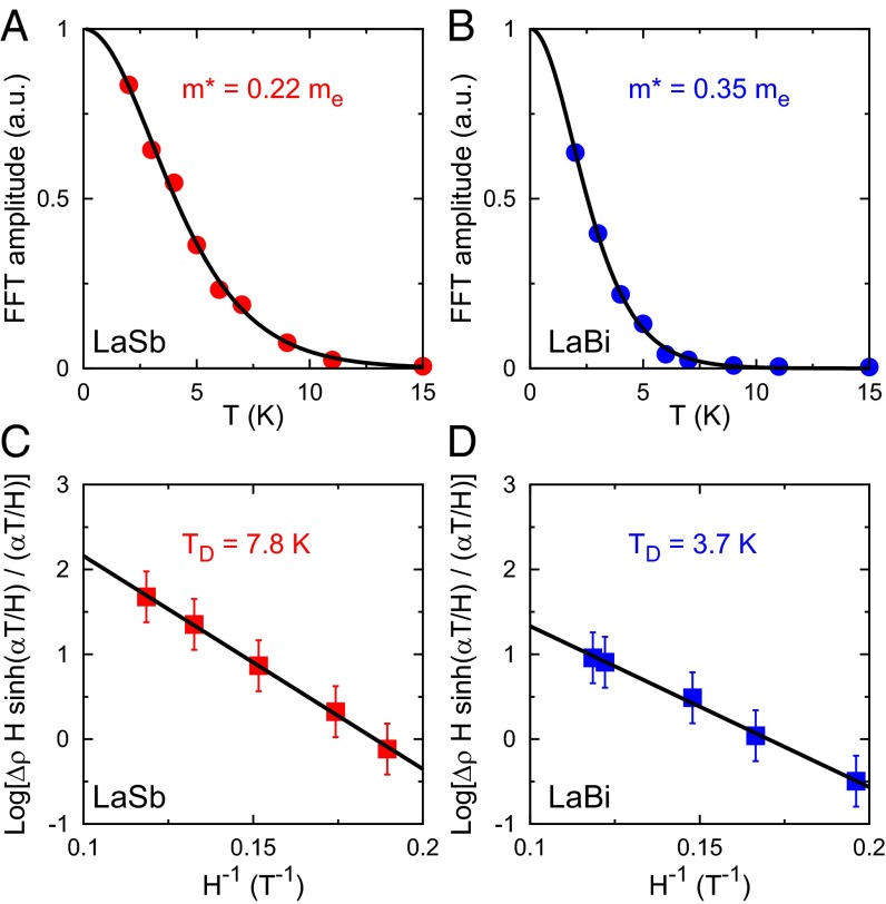
Fig. 7 A and B shows the Lifshitz−Kosevich fit (Eq. 3) to the temperature dependence of the oscillation amplitude. The resulting effective masses are for LaSb and for LaBi, in agreement with calculations and previous works (23, 24, 28, 29). Fig. 7 C and D shows the Dingle fit (Eq. 4) to the field dependence of the oscillation amplitude that determines τ, , and μ for the electron pockets in LaSb and LaBi. Table 1 summarizes all of the parameters from SdH oscillations.
Fig. 7.
(A) Amplitude of the FFT of SdH oscillations with T plotted as a function of temperature for LaSb. Solid line is a fit to the Lifshitz−Kosevich formula (Eq. 3). The effective mass of carriers is extracted from the fit and reported on the figure. (B) Lifshitz−Kosevich analysis for LaBi. Effective mass in LaBi is slightly larger than LaSb. (C) FFT amplitudes modulated by the Lifshitz−Kosevich factor plotted as a function of for LaSb. Solid line is a fit to the Dingle formula (Eq. 4). Dingle temperature is reported on the figure. (D) Dingle analysis for LaBi.
Hall Effect and Electron−Hole Compensation.
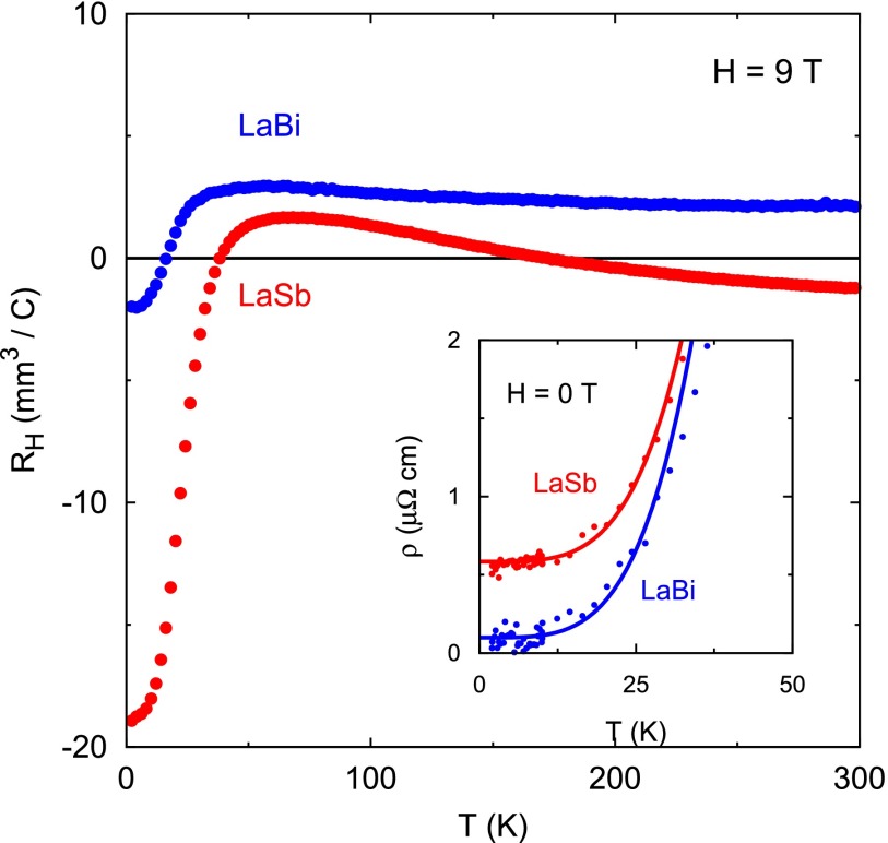
Fig. 8 shows the temperature dependence of Hall coefficient at T in LaSb (red) and LaBi (blue). Both materials show signatures of electron−hole compensation that results in a sign change in LaBi with positive above K and negative of comparable magnitude below K. LaSb shows a lesser degree of compensation, with a strong negative signal below K and a weak positive signal above K that undergoes a second sign change at K. Although LaBi has better compensation, its XMR is typically smaller than LaSb, showing that the degree of compensation does not determine the magnitude of XMR. A key factor in determining the magnitude of XMR is the small residual resistivity that minimizes the denominator in the ratio (Fig. 4C).
Fig. 8.
at T plotted as a function of temperature from to 300 K in LaSb (red) and LaBi (blue). There is one sign change in LaBi at K and two sign changes in LaSb at K and 170 K. Inset shows at T and K in LaSb and LaBi. Solid lines are fits of the form to determine μΩ⋅cm in LaSb and 0.1 in LaBi.
Our hypothesis is that the orbital texture of electron Fermi surfaces results in the small due to topological protection. It also results in the large due to the interference of magnetic field with d−p mixing. Electron−hole compensation is certainly beneficial to XMR, but it only contributes to the large , not to the small . A small is observed in all XMR materials such as WTe2 or Cd3As2. These metals are typically prone to disorder due to their large and complex unit cells, yet they have some of the smallest residual resistivity known to metals. The source of such small (high mobility) is not clear, and it is perhaps the key to understanding the origin of XMR.
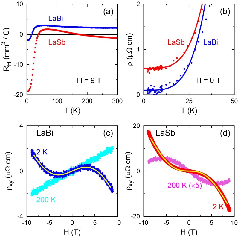
Fig. 8, Inset shows power law fits of the form to the resistivity data at low temperatures from which we extract residual resistivity μΩ⋅cm in LaBi and μΩ⋅cm in LaSb. Using the limits of and from Fig. 8, we estimate the Hall mobility from the single-band expression cm2⋅V−1⋅s−1 in LaSb and cm2⋅V−1⋅s−1 in LaBi. Single-band estimates need to be taken with caution due to the multiband nature of these materials, but, qualitatively, they show extremely high mobility in all XMR materials. In Supporting Information, we show two-band model fits to the field dependence of in both materials, from which the mobility and concentration of holes and electrons are extracted (Fig. S2 and Table S1).
Fig. S2.
Two-band model fit. (A) RH at H = 9 T plotted as a function of temperature from T = 2–300 K in LaSb (red) and LaBi (blue). There is one sign change in LaBi at T ∼ 20 K and two sign changes in LaSb at T ∼ 40 K and 170 K. (B) The ρ(T) at H = 0 T and T < 40 K in LaSb and LaBi. Solid lines are fits of the form ρ = ρ0 + AT4 to determine ρ0 = 0.6 μΩ⋅cm in LaSb and ρ0 = 0.1 μΩ⋅cm in LaBi. (C) The ρxy plotted as a function of field in LaBi from H = −9–9 T. The blue curve at T = 2 K fits to the two-band model (solid yellow line). The cyan curve at T = 200 K has a linear H dependence. (D) The ρxy plotted as a function of field in LaSb from H = −9–9 T. The red curve at T = 2 K fits to the two-band model (solid yellow line). The magenta curve at T = 200 K remains nonlinear in H. It is magnified 5× for better visibility.
Table S1.
Parameters of the two-band model fit
| Material | , cm−3 | , cm−3 | , cm2⋅V−1⋅s−1 | , cm2⋅V−1⋅s−1 |
| LaSb | ||||
| LaBi |
Discussion
Our results in LaSb and LaBi can be summarized as follows: (i) The at zero field shows a nearly perfect metal with very small (Fig. 2). (ii) The in field shows strong field-induced scattering below and a plateau below (Fig. 2). (iii) The field dependence of and constructs a triangular phase diagram (Fig. 3). (iv) The strong field-induced scattering results in XMR that correlates with RRR (Fig. 4). (v) Angle dependence of SdH oscillations fits the ellipsoidal geometry of the electron Fermi surfaces (Fig. 5). (vi) From the band structure, these electron surfaces have a mixed d−p orbital texture (Fig. 6). XMR is possibly the consequence of disturbing such orbital texture with a magnetic field. (vii) The temperature and the field dependence of the Hall Effect fit to a two-band model with near compensation, but the degree of compensation does not justify the magnitude of XMR.
These results suggest that XMR in LaSb and LaBi originates from a combination of compensated band structure and a mixed orbital texture on electron pockets. The and profiles of XMR in seemingly different topological semimetals show similar features, with a resistivity minimum at and inflection at . From the existing transport data in NbSb2 (15), PtSn4 (16), and WTe2 (12), we extract and , construct their T-H phase diagrams, and compare with the triangular phase diagram of LaBi in Fig. 9. Remarkably, the triangular phase diagram is universal to all materials with XMR, despite their chemical and structural differences. Identifying the fundamental energy scales related to and in the universal phase diagram of XMR remains an interesting open question.
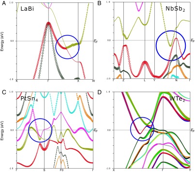
Fig. 10 shows another universal feature: The same d−p orbital texture exists in the Fermiology of other semimetals with XMR including NbSb2, PtSn4, and WTe2. Recent observations of circular dichroism by ARPES confirm such orbital mixing in WTe2 (34). Fig. 9 unifies the phenomenology of XMR in various semimetals, and Fig. 10 links XMR to a combination of electron−hole compensation and mixed orbital texture. To emphasize the role of orbital texture, we highlight observations of XMR in single-band semimetals such as Cd3As2 and Pb1-xSnxSe that, by definition, cannot be compensated (8, 35). However, both systems show large degrees of orbital mixing in their electron pockets that can interact with a magnetic field and result in the XMR. The extremely small residual resistivity of these systems ( nΩ⋅cm in Cd3As2) despite their intrinsically disordered lattices is consistent with the topological protection proposed here.
Fig. 10.
(A) Band structure of LaBi, same as in Fig. 6B. The blue circle marks the region of d−p orbital mixing. (B) Band structure of NbSb2 with a similar d−p mixing inside the blue circle. (C) Band structure of PtSn4 with similar d−p mixing. (D) Band structure of WTe2 with similar d−p mixing.
Note that two recent works have reported XMR in LaBi (36, 37). Their data are in agreement with ours.
Materials and Methods
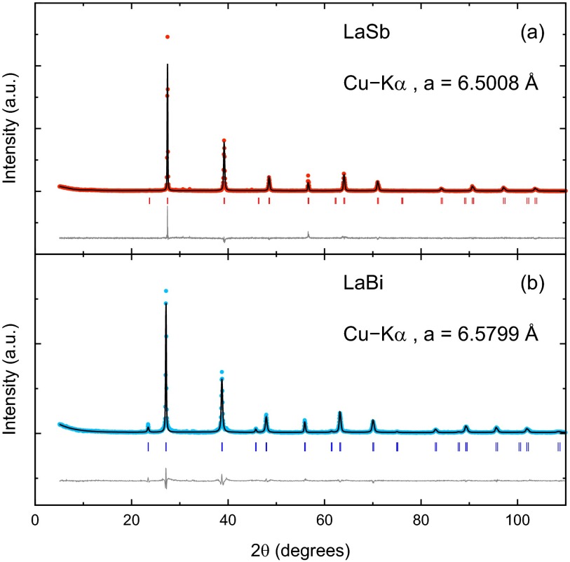
Single crystals of LaBi were grown using Indium flux. The starting elements La:Bi:In = 1:1:20 with purity were placed in an alumina crucible inside an evacuated quartz tube. The mixture was heated to 1,000 °C, slowly cooled to 700 °C, and finally decanted in a centrifuge. A similar procedure was used to grow single crystals of LaSb from tin flux. Energy-dispersive X-ray spectroscopy on each sample confirmed a 1:1 ratio of lanthanum to pnictogen with error. Powder X-ray diffraction for both systems are presented in Supporting Information and Fig. S3. Resistivity measurements were performed in a Quantum Design Physical Property Measurement System using a standard four-probe method. Hall voltages were measured with transverse contacts in negative and positive fields, with the data antisymmetrized to calculate the transverse resistivity and the Hall coefficient . The LaSb single crystal had residual resistivity μΩ⋅cm and RRR 170. The LaBi crystal had μΩ⋅cm and RRR = 610.
Fig. S3.
X-ray refinements. (A) Rietveld refinement (solid black line) on the powder XRD data for LaSb (red). Lattice parameter from the refinement is given on the figure. (B) Rietveld refinement (solid black line) on the powder XRD data for LaBi (blue).
Low-Temperature Heat Capacity Data
To rule out an MIT at , we measured the heat capacity of LaSb down to 0.5 K in a Helium 3 fridge. , where is the density of states at the Fermi level. Fig. S1 shows no difference between as a function of at H = 0 and at H = 9 T; therefore, the magnetic field does not change the density of states. This rules out the opening of a field-induced gap that would result in a significant drop in .
Two-Band Model Fit to Hall Data
Fig. S2 shows the temperature and field dependence of RH. Fig. S2 A and B restates the temperature dependence of RH and resistivity as given in Fig. 8. Fig. S2 C and D shows the field dependence of with fits to the two-band model according to
We forced the fit to capture both and . The resulting values for electron and hole concentration and mobility are given in Table S1.
Note that the parameters from the fit could differ from the more accurate results we report in Table 1 from quantum oscillations. There are, in fact, three bands in LaSb and LaBi, so the fit may not be completely accurate, but it certainly shows that (i) both systems are fairly compensated and (ii) compensation is better in LaBi. However, XMR does not rely on the degree of compensation as discussed in the main text (Fig. 8). It mainly relies on how small is.
Acknowledgments
We thank G. Grissonanche, S. R. Julian, and L. Muechler for helpful discussions. This research was supported by the Gordon and Betty Moore Foundation under the EPiQS program, Grant GBMF 4412. S.K. is supported by the ARO MURI on topological insulators, Grant W911NF-12-1-0461.
Footnotes
Conflict of interest statement: R.J.C. and A. D. Bianchi have appeared as coauthors in a different topic area in the previous publication by Fennell A, et al. (2014) Evidence for SrHo2 O4 and SrDy2 O4 as model J1-J2 zigzag chain materials. Phys Rev B 89(22):224511. In that collaboration, samples synthesized in R.J.C. laboratory by T. Klimczuk were sent directly to M. Kenzelman for experimental study. R.J.C., Bianchi, and Kenzelman work at separate institutions and R.J.C. and Bianchi did not have any contact during the course of that work.
This article contains supporting information online at www.pnas.org/lookup/suppl/doi:10.1073/pnas.1607319113/-/DCSupplemental.
References
- 1.Daughton JM. GMR applications. J Magn Magn Mater. 1999;192(2):334–342. [Google Scholar]
- 2.Rao CNR, Cheetham AK. Giant magnetoresistance in transition metal oxides. Science. 1996;272(5260):369–370. [Google Scholar]
- 3.Wolf SA, et al. Spintronics: A spin-based electronics vision for the future. Science. 2001;294(5546):1488–1495. doi: 10.1126/science.1065389. [DOI] [PubMed] [Google Scholar]
- 4.Lenz J. A review of magnetic sensors. Proc IEEE. 1990;78(6):973–989. [Google Scholar]
- 5.Jankowski J, El-Ahmar S, Oszwaldowski M. Hall sensors for extreme temperatures. Sensors (Basel) 2011;11(1):876–885. doi: 10.3390/s110100876. [DOI] [PMC free article] [PubMed] [Google Scholar]
- 6.Ramirez AP. Colossal magnetoresistance. J Phys Condens Matter. 1997;9(39):8171–8199. [Google Scholar]
- 7.Xiong J, et al. Evidence for the chiral anomaly in the Dirac semimetal Na3Bi. Science. 2015;350(6259):413–416. doi: 10.1126/science.aac6089. [DOI] [PubMed] [Google Scholar]
- 8.Liang T, et al. Ultrahigh mobility and giant magnetoresistance in the Dirac semimetal Cd3As2. Nat Mater. 2015;14(3):280–284. doi: 10.1038/nmat4143. [DOI] [PubMed] [Google Scholar]
- 9.Shekhar C, et al. Extremely large magnetoresistance and ultrahigh mobility in the topological Weyl semimetal candidate NbP. Nat Phys. 2015;11(8):645–649. [Google Scholar]
- 10.Ghimire NJ, et al. Magnetotransport of single crystalline NbAs. J Phys Condens Matter. 2015;27(15):152201. doi: 10.1088/0953-8984/27/15/152201. [DOI] [PubMed] [Google Scholar]
- 11.Huang X, et al. Observation of the chiral-anomaly-induced negative magnetoresistance in 3d Weyl semimetal TaAs. Phys Rev X. 2015;5(3):031023. [Google Scholar]
- 12.Ali MN, et al. Large, non-saturating magnetoresistance in WTe2. Nature. 2014;514(7521):205–208. doi: 10.1038/nature13763. [DOI] [PubMed] [Google Scholar]
- 13.Ali MN, et al. Correlation of crystal quality and extreme magnetoresistance of WTe2. Europhys Lett. 2015;110(6):67002. [Google Scholar]
- 14.Zhu Z, et al. Quantum oscillations, thermoelectric coefficients, and the fermi surface of semimetallic WTe2. Phys Rev Lett. 2015;114(17):176601. doi: 10.1103/PhysRevLett.114.176601. [DOI] [PubMed] [Google Scholar]
- 15.Wang K, Graf D, Li L, Wang L, Petrovic C. Anisotropic giant magnetoresistance in NbSb2. Sci Rep. 2014;4:7328. doi: 10.1038/srep07328. [DOI] [PMC free article] [PubMed] [Google Scholar]
- 16.Mun E, et al. Magnetic field effects on transport properties of PtSn4. Phys Rev B. 2012;85(3):035135. [Google Scholar]
- 17.Tafti FF, Gibson QD, Kushwaha SK, Haldolaarachchige N, Cava RJ. Resistivity plateau and extreme magnetoresistance in LaSb. Nat Phys. 2016;12(3):272–277. [Google Scholar]
- 18.Zeng M, et al. 2015. Topological semimetals and topological insulators in rare earth monopnictides. arXiv:1504.03492.
- 19.Thoutam L, et al. Temperature-Dependent three-dimensional anisotropy of the magnetoresistance in WTe2. Phys Rev Lett. 2015;115(4):046602. doi: 10.1103/PhysRevLett.115.046602. [DOI] [PubMed] [Google Scholar]
- 20.Wang YL, et al. Origin of the turn-on temperature behavior in WTe2. Phys Rev B. 2015;92(18):180402. [Google Scholar]
- 21.Deacon JM, Mackinnon L. Ultrasonic quantum oscillations in white tin. J Phys F Met Phys. 1973;3(12):2082–2091. [Google Scholar]
- 22.Cowey JE, Gerber R, Mackinnon L. Quantum oscillations in ultrasonic absorption and the Fermi surface of indium. J Phys F Met Phys. 1974;4(1):39. [Google Scholar]
- 23.Kitazawa H, et al. DE Haas-van Alphen effects on La(Sb, Bi) and Ce(Sb, Bi) J Magn Magn Mater. 1983;31-34(Part 1):421–422. [Google Scholar]
- 24.Hasegawa A. Fermi Surface of LaSb and LaBi. J Phys Soc Jpn. 1985;54(2):677–684. [Google Scholar]
- 25.Ren Z, Taskin AA, Sasaki S, Segawa K, Ando Y. Large bulk resistivity and surface quantum oscillations in the topological insulator Bi2Te2Se. Phys Rev B. 2010;82(24):241306. [Google Scholar]
- 26.Li G, et al. Two-dimensional Fermi surfaces in Kondo insulator SmB6. Science. 2014;346(6214):1208–1212. doi: 10.1126/science.1250366. [DOI] [PubMed] [Google Scholar]
- 27.Tan BS, et al. Unconventional Fermi surface in an insulating state. Science. 2015;349(6245):287–290. doi: 10.1126/science.aaa7974. [DOI] [PubMed] [Google Scholar]
- 28.Settai R, et al. Acoustic de Haas-Van Alphen effect in LaSb and CeSb. Physica B. 1993;186:176–178. [Google Scholar]
- 29.Yoshida M, et al. Cyclotron resonance of LaBi. J Phys Soc Jpn. 2001;70(7):2078–2081. [Google Scholar]
- 30.Blaha P, Schwarz K, Madsen G, Kvasnicka D, Luitz J. 2001. WIEN2K, An Augmented Plane Wave + Local Orbitals Program for Calculating Crystal Properties, ed Schwarz K (Tech Univ Wien, Vienna)
- 31.McCann E, et al. Weak-localization magnetoresistance and valley symmetry in graphene. Phys Rev Lett. 2006;97(14):146805. doi: 10.1103/PhysRevLett.97.146805. [DOI] [PubMed] [Google Scholar]
- 32.Bai J, et al. Very large magnetoresistance in graphene nanoribbons. Nat Nanotechnol. 2010;5(9):655–659. doi: 10.1038/nnano.2010.154. [DOI] [PMC free article] [PubMed] [Google Scholar]
- 33.Xu X, Yao W, Xiao D, Heinz TF. Spin and pseudospins in layered transition metal dichalcogenides. Nat Phys. 2014;10(5):343–350. [Google Scholar]
- 34.Jiang J, et al. Signature of strong spin-orbital coupling in the large nonsaturating magnetoresistance material WTe2. Phys Rev Lett. 2015;115(16):166601. doi: 10.1103/PhysRevLett.115.166601. [DOI] [PubMed] [Google Scholar]
- 35.Liang T, et al. Evidence for massive bulk Dirac fermions in Pb1-xSnxSe from Nernst and thermopower experiments. Nat Commun. 2013;4(4):2696. doi: 10.1038/ncomms3696. [DOI] [PubMed] [Google Scholar]
- 36.Sun S, Wang Q, Guo PJ, Liu K, Lei H. 2016. Large magnetoresistance in LaBi: Origin of field-induced resistivity upturn and plateau in compensated semimetals. arXiv:1601.04618.
- 37.Kumar N, et al. 2016. Observation of quasi-two-dimensional electron transport in the topological semimetal LaBi. arXiv:1601.07494.


