

Researchers report an organic nanowire artificial synapse that emulates working principles and energy consumption of biological synapses.
Keywords: artificial synapse, organic nanowire, energy consumption, organic electronics, bio-inspired electronics, short-term plasticity, long-term plasticity
Abstract
Emulation of biological synapses is an important step toward construction of large-scale brain-inspired electronics. Despite remarkable progress in emulating synaptic functions, current synaptic devices still consume energy that is orders of magnitude greater than do biological synapses (~10 fJ per synaptic event). Reduction of energy consumption of artificial synapses remains a difficult challenge. We report organic nanowire (ONW) synaptic transistors (STs) that emulate the important working principles of a biological synapse. The ONWs emulate the morphology of nerve fibers. With a core-sheath–structured ONW active channel and a well-confined 300-nm channel length obtained using ONW lithography, ~1.23 fJ per synaptic event for individual ONW was attained, which rivals that of biological synapses. The ONW STs provide a significant step toward realizing low-energy–consuming artificial intelligent electronics and open new approaches to assembling soft neuromorphic systems with nanometer feature size.
INTRODUCTION
Synapses are among the most important functional units for learning and memory (1, 2). They consume an extremely small amount of energy (10 fJ per synaptic event), so a human brain consumes only as much energy as a domestic lightbulb but can outperform a supercomputer in many aspects. Recently, great efforts have been made to develop synapse-emulating circuits (3) and electronic devices (4–6), but they still consume orders of magnitude more energy (generally above picojoule level) than do natural synapses (7–11). Solving these problems requires appropriate choice of materials and design of devices; these remain difficult challenges.
Here, we focus on design and fabrication of an artificial synapse. Attaining this goal presents several challenges: the first is to select a material that mimics the morphology of nerve fibers that form synaptic junction. We selected organic nanowires (ONWs) because they mimic nerve fiber morphology in terms of elongated shape, flexibility, and good scalability to large areas, which enable formation of a three-dimensional grid of crisscrossing alignment of nerve fibers in a human brain (12). This is the first morphological emulation of nerve fibers for use in an artificial synapse, which has great potential in various soft bio-inspired and bio-integrated electronics (13–18). The second challenge is to design a material structure that can emulate, in a single device, the important working principles of a synapse. Considering the distinct reversibility of trapping and detrapping ions in different polymer matrices, ONWs with the structure of a polyethylene oxide (PEO) sheath wrapped around a poly(3-hexylthiophene-2,5-diyl) (P3HT) core were fabricated to facilitate the development of short-term and long-term plasticity. Furthermore, we aimed to achieve an artificial synapse that has energy consumption comparable to that of a biological synapse. This low energy consumption is essential to constructing highly integrated, very large-scale neuromorphic computing systems. With a nanowire lithographic 300-nm channel length, ~1.23 fJ per synaptic event was attained, which is the lowest attained so far and even rivals that of biological synapses.
RESULTS AND DISCUSSION
We designed ONW synaptic transistor (ST) architecture to emulate the functions of a biological synapse (Fig. 1). A typical ONW ST was composed of a conducting line probe (A′), an ion gel, an ONW (B′), and two metal contact pads on a substrate (fig. S1). The conducting line probe (A′), which mimicked a biological axon and a presynaptic membrane, was in contact with the ion gel to supply signals analogous to presynaptic spikes (fig. S2). The ion gel provided mobile ions that migrate in response to the presynaptic spikes. The ion gel between the probe and ONW emulates the synaptic cleft, which is ionically conductive to allow chemical transmission across it but is electrically insulating to separate electrical input and output and thereby to ensure that synaptic processes can occur independently at the presynaptic membrane and postsynaptic membrane. The core-sheath ONW (B′) has a P3HT inner core in a PEO sheath (fig. S3). The ONW combined with a drain electrode mimics a biological dendrite (B). The core-sheath structure of ONW underlies the mechanism of short-term and long-term plasticity in the artificial synapse. The presynaptic spikes provide an electrical field that helps ions penetrate the PEO sheath or even the P3HT core. The process in which ions penetrate the PEO sheath under presynaptic spikes and later rapidly diffuse back to the ion gel induces short-term plasticity. A number of consecutive presynaptic spikes increase the depth to which ions penetrate into the P3HT core, in which ions have low solubility and cannot easily diffuse back to the ion gel spontaneously; this restricted mobility induces long-term potentiation (LTP) (fig. S4). Here, gold electrodes were used for electrical connections, and a SiO2-coated Si substrate was used to provide physical support for the device. Our homebuilt electrohydrodynamic NW (e-NW) printer rapidly and inexpensively fabricated ONWs on a large scale while simultaneously controlling the location and alignment of individual ONWs (19). The spacing of ONWs was computer-controlled (fig. S5). The diameter of ONWs could be controlled by adjusting the solution concentration (fig. S6). The printing technique can print ONWs of other types of polymer semiconductor materials (fig. S7).
Fig. 1. Schematic of biological neuronal network and an ONW ST that emulates a biological synapse.
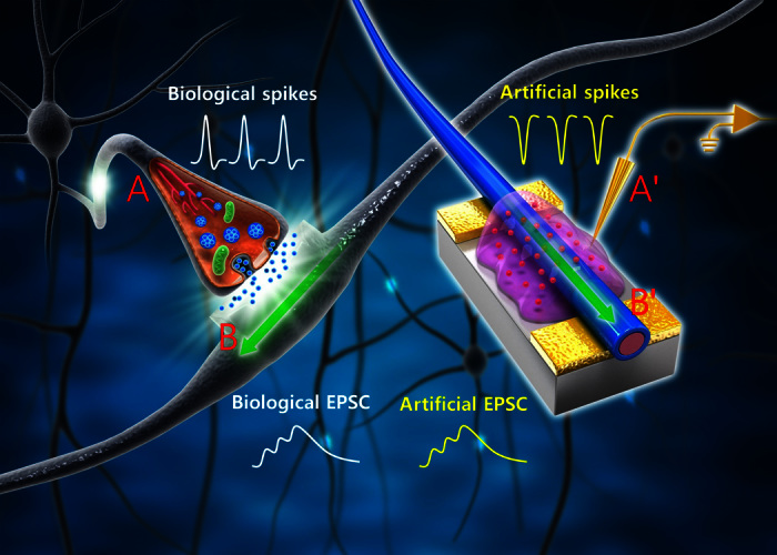
The conductive lines and probe (A′) mimic an axon (A) that delivers presynaptic spikes from a preneuron to the presynaptic membrane. The mobile ions in the ion gel move in the electrical field analogous to the neuron transmitters in the synaptic cleft that later induces an excitatory postsynaptic current (EPSC) in the dendrite through the contact of postsynaptic membrane. An ONW (B′) combined with a drain electrode mimics a biological dendrite (B). EPSC is generated in the ONW in response to presynaptic spikes and is delivered to a postneuron through connections to the drain electrode.
A biological synapse permits a neuron to pass an electrical or chemical signal to another cell (20). Synapses are widely believed to contribute to the formation of memory, and the synaptic strength is thought to result in the storage of information by changing the amplitude of a postsynaptic current. A brief application (presynaptic spike) of voltage (−1 V, 50 ms) on the ion gel triggered an excitatory postsynaptic current (EPSC), which reached a peak value of 3.82 nA, and then gradually decayed to a resting current of ~1 nA (Fig. 2, A to C). This trend emulates a biological process, in which a neuron generates an action potential (spike) that propagates along the axon and is transmitted across a synapse to the next neuron. This behavior in the device originates from ion migration in the ion gel (fig. S4, A to C). Before the spike, anions and cations are distributed randomly. A negative presynaptic spike causes anions to accumulate at the ion gel–ONW interface during the spike; the high density of anions surrounding the NW attracts a certain number of holes in the P3HT channel, which move in response to a driving voltage to form an EPSC. After the spike, the distribution of anions returns to random, and the EPSC gradually decays. Analogously, inhibitory postsynaptic current (IPSC) was triggered by a positive presynaptic spike (Fig. 2D). EPSC and IPSC are complementary processes that underlie the basic features of neuronal transmission.
Fig. 2. Short-term synaptic plasticity.
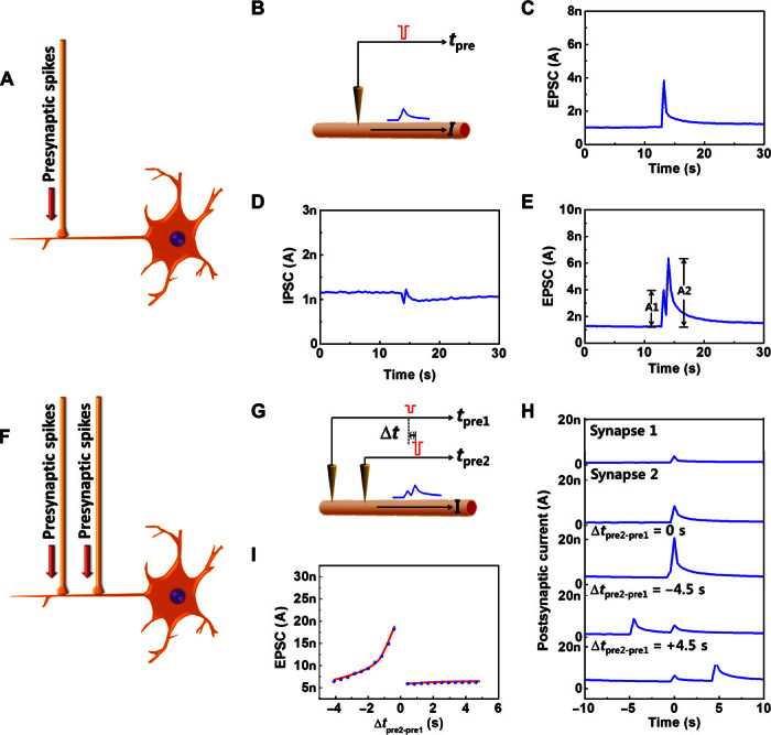
(A) Schematic of application of presynaptic spikes to a postneuron through a synaptic joint. (B) Schematic of application of electrical pulses to an ONW ST analogous to presynaptic spikes that induces current responses through the ONW active channel. (C) EPSC triggered by a negative presynaptic spike (−1 V, 50 ms). (D) IPSC triggered by a positive presynaptic spike (1 V, 50 ms). (E) EPSCs triggered by two spikes, with an interspike interval of 780 ms. A1 and A2, amplitudes of the first and second EPSCs, respectively. (F) Schematic of applying spatiotemporally correlated presynaptic spikes onto a postneuron through two presynaptic connections to one single strand of dendrite. (G) Schematic of EPSC triggered by a pair of spatiotemporally correlated spikes applied to an ONW ST through two laterally coupled gates. (H) EPSC triggered by a single or pair of spatiotemporally correlated presynaptic spikes versus time. (I) Amplitude of the EPSC at t = 0 (when the spike is applied to synapse 1) versus interval Δtpre2 − pre1 between the spikes.
The change in the strength of a synapse’s response over time in response to external stimuli is referred to as synaptic plasticity and is regarded as an important foundation of learning and memory. Short-term plasticity can either strengthen or weaken a synapse for a short time on scales from tens of milliseconds to a few minutes. Short-term synaptic enhancement can be attained when two spikes arrive in rapid succession (Fig. 2E) (21). It is involved in encoding temporal information in auditory and visual signals (22) and has an important function in associative learning, information processing, pattern recognition, and sound source localization (2, 23–25). Although many biological mechanisms remain unclear, for example, how exactly short-term plasticity is involved in pattern recognition and associative learning, scientists continue to apply existing knowledge to achieve some of these functions in artificial systems (4, 25, 26). Short-term synaptic enhancement was successfully mimicked in our ONW ST by applying two consecutive negative presynaptic spikes with an interspike interval (780 ≤ Δtpre ≤ 7800 ms). The amplitude of the second EPSC peak (A2) was 1.62 times the amplitude triggered by the first spike (A1) (Fig. 2E). The increase in A2 was caused by residual ions that had accumulated during the first spike. Some of these ions accumulated near the ONW–ion gel interface and added to the total amount of ions accumulated during the second-spike period. The quantity of residual ions increased as Δtpre decreased, thereby increasing the summation of EPSCs. The A2/A1 ratio decreased as Δtpre increased (fig. S8). This spontaneous decay of current retention can be regarded as analogous to loss of memory by a human brain because the EPSC trends fit very well with a forgetting curve (y = b × t−m) (fig. S9). Comparably, further decreased IPSC was also obtained by applying additional positive pulses (fig. S10).
Excitatory and inhibitory synapses exhibit enhancement and depression, the combined use of which underlies short-term memory. Spatiotemporally correlated stimuli from different presynapses could be used to trigger a postsynaptic current to establish dynamic logic in a neural network. The basic spatiotemporal dynamic logic was demonstrated in a simple structure that uses an ONW ST with two laterally coupled gates (Fig. 2, F and G). EPSC responses were recorded under a constant source-drain voltage of 0.75 V. A single spike on presynapse 1 (−1 V, 50 ms) triggered EPSC 1 with an amplitude of ~4 nA; a single spike on presynapse 2 (−2 V, 50 ms) triggered EPSC 2 with an amplitude of ~6 nA (Fig. 2H). When presynaptic spike 1 and presynaptic spike 2 were applied sequentially with an interspike interval (Δtpre2 − pre1), the accumulation of migrated ions caused the EPSC 2 induced by the second spike to be superimposed onto the EPSC 1 induced by the first spike; as a result, the total amplitude of EPSC increased. When Δtpre2 − pre1 = 0, the EPSC 1 and EPSC 2 were triggered simultaneously and resulted in a maximum EPSC of ~22 nA in the postsynapse. The EPSC amplitude at the end of the presynaptic spike 1 (set as t = 0, where EPSC summation was recorded) was plotted as a function of Δtpre2 − pre1 to understand the influence of a spike on a correlated presynapse (Fig. 2I). The amplitude of EPSC at t = 0 is consistent with the peak amplitude of the EPSC 1 if the EPSC 2 were triggered afterward (Δtpre2 − pre1 > 0). However, when EPSC 2 was triggered before EPSC 1 (Δtpre2 − pre1 < 0), EPSC at t = 0 became the superimposition of EPSC 1 and the remaining EPSC 2. This is similar to the neural response to spatiotemporally correlated stimuli from different presynapses.
Long-term plasticity that usually occurs at excitatory synapses includes LTP and long-term depression (LTD) (27), which are respectively a persistent increase and a persistent decrease in synaptic strength, following a number of consecutive stimulations of a synapse. Because memories are thought to be encoded by modification of synaptic strength (28), LTP is widely regarded as a mechanism that underlies learning and memory in the brain (22). LTP in the ONW ST was demonstrated by applying an increased number of presynaptic spikes (Fig. 3A); after this treatment, the EPSC increased by as much as ~15 times and was ~1.5 times the resting current 5 min after the spikes. LTP tends to greatly increase electrical responses of neurons to stimuli, and this increase (“potentiation”) in synaptic strength lasts much longer than do other processes that affect synaptic strength. In contrast, LTD selectively weakens specific synapses, may prevent synaptic strength from reaching some level of maximum efficacy that results from simply continued LTP, and inhibits encoding of new information (29). LTD was obtained by applying consecutive positive synaptic spikes (Fig. 3B). The mimicking of short-term and long-term plasticity in a single ONW ST has potential in constructing spiking neural network, which adapts to real-time functions, for example, real-time pattern recognition (4, 25).
Fig. 3. Long-term synaptic plasticity.

(A) Postsynaptic current versus time stimulated by 30 presynaptic spikes (−1 V, 50 ms) of the ONW ST; VD (driving voltage) = 0.75 V. (B) Postsynaptic current versus time stimulated by 30 presynaptic spikes (1 V, 50 ms) of the ONW ST, VD = 0.75 V. (C) Postsynaptic current triggered by 60 negative and 60 positive pulses. (D) Postsynaptic current as a function of nonlinear presynaptic spikes.
Application of approximately 60 cycles of negative spikes increased the EPSC amplitude by 22 times; to reduce the ONW conductance back to the initial value, 60 positive pulses were required (Fig. 3C). The results suggest that the present configuration of the ONW device can simulate the analog storage capacity of synapses. When a series of negative (or positive) spikes were applied, the negative ions continuously accumulated toward (or away from) the conductive channel, resulting in significant potentiation (or depression). The change rate in the synaptic strength increased with the number of spikes. However, when 60 negative (or positive) presynaptic spikes were applied, the postsynaptic current tended to saturate without further significant change due to a newly established equilibrium of ion movement. The negative presynaptic spikes drove the mobile ions to near the channel region, but the residual accumulated ions tended to drift back during the interval between the presynaptic spikes. These two trends coexisted because of the fixed number of mobile ions in the ion gel matrix. We hypothesize that the rates of the two opposite trends of ion movement became equal when sufficient ions were urged to approach the channel region by a certain number of presynaptic spikes and that at this point, equilibrium was finally established so that no further significant increase in EPSC was observed. Among simulations of various synaptic behaviors, symmetry characteristics of potentiation and depression were found to be the most important requirement. To improve the symmetry in the curve, we applied nonidentical presynaptic spikes and observed significant improvement in symmetry (Fig. 3D). Spike timing–dependent plasticity (STDP), which describes the change of synaptic weight depending on relative timing of the spikes of pre- and postneurons, is an important synaptic adaption rule of Hebbian learning. A typical asymmetric form of STDP (fig. S11, A and B) was obtained using an ONW ST, which could be useful in the construction of a network (30–32).
Ultralow energy consumption is one of the most important superiorities of a neural system; to achieve this, different types of electronic devices have been investigated. Although some of those have shown picojoule-level energy consumptions, further reducing synaptic energy to the femtojoule level remains a challenging task, but is an important requirement for the construction of very large systems. To achieve significantly reduced energy consumption, we used polyvinyl carbazole (PVK) ONWs as lithographic tools to produce a narrow gap of ~300 nm between electrodes to provide a short channel length (fig. S12, A to C). Synaptic enhancement and depression of a nanogap ONW ST were also demonstrated from consecutive small presynaptic spikes (−1 mV) (Fig. 4A). Energy consumption was estimated as E = AIW, where A = 20 mV is the drain voltage, I = 5.52 pA is the current flowing across the device, and W = 111.2 ms is the width of the programming pulse. The minimum E for the 10-ONW artificial synapses with nanogap (fig. S12D) was ~12.3 fJ per spike, so the average energy consumption was ~1.23 fJ per spike for each NW. This value is orders of magnitude lower than those of currently available synapse-inspired electronic devices (Fig. 4B) and rivals that of biological synapses. This result shows that these ONW STs have the potential to mimic the low energy consumption of a biological synapse in a human brain, in which each spike has an average frequency of ~10 Hz with an amplitude of ~100 mV, and each synaptic event has a duration of ~100 ms, and consumes energy on a scale of ~10 fJ (33). The low energy consumption of the devices is a benefit of (i) the large surface-to-volume ratio of ONWs that improves the contact area between ONWs and surrounding ion gel and (ii) the short channel length that significantly shortens the path along which energy can dissipate (fig. S13 and related discussion) (34). The ion gel is ionically conductive and electrically insulating, with leakage current orders of magnitude smaller than that of the semiconducting path in similar transistor geometries (19), so energy dissipation through the ionic gating is negligible (19, 35). Spike rate was correlated with EPSC in the short-channel ST (fig. S14). EPSC could also be increased by applying large-amplitude presynaptic spikes (fig. S15) or longer-time stimulation (fig. S16), but this approach requires increase in energy consumption. Narrow pulse width that is in the reasonable range of dopaminergic neurons in the central brain also triggered EPSC in ONW STs (fig. S17). Furthermore, large-scale 144 STs were fabricated on a 4-inch wafer using the highly aligned ONWs (Fig. 4C). To study the transparency of ONWs, we compared the transmittance of bare polyethylene terephthalate (PET) (red) and PET covered with 50-μm–pitched ONWs (blue). The 50-μm–pitched ONW coverage reduced transparency by <1% (Fig. 4D). The photograph (inset of Fig. 4D) showed no obvious reduction in the transparency of PET by the ONW coverage. Our e-NW printing technique that precisely aligns ONWs on an extended area ensures individually addressable synaptic device arrays and low-cost rapid fabrication of large-area electronics. This type of device has a transistor structure, and transfer and output characteristics can be recorded (fig. S19).
Fig. 4. Special features: Low energy consumption, scalability and transparency.

(A) EPSC triggered by an even lower-intensity negative presynaptic spike and short-term synaptic enhancement by two negative pulses. (B) Energy consumption per synaptic event of current available synaptic devices. NG, nanogap; PCM, phase change memory; RRAM, resistive switching random access memory. (C) Array of 144 ONW STs fabricated on a 4-inch silicon wafer. Inset: Scanning electron microscopy (SEM) image of a typical ONW with a diameter of 200 nm. (D) Ultraviolet–visible light spectroscopy as a measure of the transparency of bare and ONW array–loaded PET sheets. Inset: Photograph of a bare PET sheet and a 50-μm–pitched ONW array–loaded PET sheet.
CONCLUSION
In conclusion, we used ONW-based electronic devices to emulate the morphology, working principles, and energy consumption of synaptic junctions of nerve fibers. Important working principles, such as short-term plasticity, LTP, and LTD, were emulated in a single electronic device. These properties are essential for pattern recognition and associative learning. Extremely low energy consumption of the artificial synapses was realized by using core-sheath–structured ONWs across a short nanochannel. The femtojoule-level energy consumption (~1.23 fJ per synaptic event) rivals that of biological synapses (~10 fJ per synaptic event), and this achievement is a significant step toward fabrication of brain-inspired electronic devices. This work presents important progress in the development of high-density and soft brain-inspired computational systems that consume ultralow amounts of energy.
MATERIALS AND METHODS
Fabrication of highly aligned ONWs
P3HT [regioregularity, ~90%; weight-average molecular weight (Mw), ~45,570; Sigma-Aldrich] and PEO (Mw, ~400,000; Sigma-Aldrich) were used to prepare 70:30 (w/w) blend solutions of P3HT/PEO. Trichloroethylene and chlorobenzene were mixed (1:1.5, w/w) and used as the cosolvent of the P3HT/PEO blend. The blended solution was injected through a metal nozzle at a feed rate of 800 nl min−1, and ONWs were formed and aligned on the substrate by using a homebuilt e-NW printer. The nozzle tip-to-collector distance was ~6.5 mm, and 3.2 kV was applied to the nozzle.
Device fabrication
P3HT/PEO-blend ONWs were drawn on predeposited Ti/Au source–drain patterns using our home built e-NW printer, which consists of two major components: an injector and a collector (fig. S1). The injected polymer solution was stretched into fibers in a high electric field to arrive at the collector, which was mounted horizontally and can move horizontally with digitally controlled speed and direction to adapt to the injection speed of the rapidly formed ONWs and to align the ONWs in desired patterns. Ion gel liquid composed of poly(styrene-block-methyl methacrylate-block-styrene) (PS-PMMA-PS) triblock copolymer (36) and 1-ethyl-3-methylimidazolium bis(trifluoromethyl sulfonyl) imide in ethyl acetate (0.7:9.3:90, w/w/w ratio) was drop-cast to the channel region and vacuum-annealed for 1 hour at room temperature to assist removal of solvent and formation of gel-like films with physical association of the PS blocks.
Characterization
SEM imaging was performed using a JEOL-6500 field emission microscope. High-resolution transmission electron microscopy with electron energy loss spectroscopy results was obtained using the JEOL JEM-2200FS at the National Institute for Nanomaterials Technology (Pohang, Republic of Korea). All electrical transport properties were tested using a probe station in an N2-filled glove box using a Keithley 4200 semiconductor parameter analyzer.
Supplementary Material
Acknowledgments
Funding: This research was supported by the Pioneer Research Center Program through the National Research Foundation of Korea funded by the Ministry of Science, ICT and Future Planning (2012-0009460) and by the Center for Advanced Soft Electronics funded by the Ministry of Science, ICT and Future Planning as Global Frontier Project (2014M3A6A5060947). Author contributions: W.X. conducted most of the experiments, including fabrication of devices and analysis of data. S.-Y.M. contributed to the fabrication of NW. All authors (W.X., S.-Y.M., H.H., and T.-W.L.) contributed to the discussion of the results. T.-W.L. initiated the study. W.X. and T.-W.L. wrote the paper. Competing interests: The authors declare that they have no competing interests. Data and materials availability: All data needed to evaluate the conclusions in the paper are present in the paper and/or the Supplementary Materials. Additional data related to this paper may be requested from the authors.
SUPPLEMENTARY MATERIALS
Supplementary material for this article is available at http://advances.sciencemag.org/cgi/content/full/2/6/e1501326/DC1
fig. S1. Schematic of the scalable fabrication of the ion gel–gated ONW ST arrays.
fig. S2. Schematic of electrical characterization.
fig. S3. Core-sheath structure of the ONWs.
fig. S4. Schematic of the ion migration in the ion gel and charge carriers in ONW for short-term and long-term plasticity.
fig. S5. Control over inter-ONW spacing.
fig. S6. Control over ONW diameter.
fig. S7. SEM image of aligned N2200/PVK (7:3) polymer semiconductor NWs.
fig. S8. Short-term synaptic enhancement.
fig. S9. Current-retention behavior fits well with the curve of forgetting.
fig. S10. Further decreased IPSC was observed with an increased number of presynaptic spikes.
fig. S11. Spike timing–dependent plasticity.
fig. S12. SEM images for the nanogap formation.
fig. S13. Configuration of a typical ion gel–gated ONW ST.
fig. S14. Spike rate–dependent plasticity of a short-channel ST.
fig. S15. Presynaptic spike voltage–dependent EPSC behavior of the ONW ST.
fig. S16. Presynaptic spike duration–dependent EPSC behavior of the ONW ST.
fig. S17. Postsynaptic current in ONW ST triggered by 8-ms pulses.
fig. S18. Data selection for SNR calculation.
fig. S19. Transistor characteristics of the electronic devices.
REFERENCES AND NOTES
- 1.Ho V. M., Lee J.-A., Martin K. C., The cell biology of synaptic plasticity. Science 334, 623–628 (2011). [DOI] [PMC free article] [PubMed] [Google Scholar]
- 2.Abbot L. F., Regehr W. G., Synaptic computation. Nature 431, 796–803 (2004). [DOI] [PubMed] [Google Scholar]
- 3.Mahowald M., Douglas R., A silicon neuron. Nature 354, 515–518 (1991). [DOI] [PubMed] [Google Scholar]
- 4.Ohno T., Hasegawa T., Kazuya T., Gimzewksi J. K., Aono M., Short-term plasticity and long-term potentiation mimicked in single inorganic synapses. Nat. Mater. 10, 591–595 (2011). [DOI] [PubMed] [Google Scholar]
- 5.Chanthbouala A., Garcia V., Cherifi R. O., Bouzehouane K., Fusil S., Moya X., Xavier S., Yamada H., Deranlot C., Mathur N. D., Bibes M., Barthélémy A., Grollier J., A ferroelectric memristor. Nat. Mater. 11, 860–864 (2012). [DOI] [PubMed] [Google Scholar]
- 6.Pickett M. D., Medeiros-Ribeiro G., Williams R. S., A scalable neuristor built with Mott memristors. Nat. Mater. 12, 114–117 (2013). [DOI] [PubMed] [Google Scholar]
- 7.Hasegawa T., Ohno T., Terabe K., Nakayama T., Gimzewski J. K., Aono M., Learning abilities achieved by a single solid-state atomic switch. Adv. Mater. 22, 1831–1834 (2010). [DOI] [PubMed] [Google Scholar]
- 8.Jo S. H., Chang T., Ebong I., Bhadviya B. B., Mazumder P., Lu W., Nanoscale memristor device as synapse in neuromorphic systems. Nano Lett. 10, 1297–1301 (2010). [DOI] [PubMed] [Google Scholar]
- 9.Kuzum D., Jeyasingh R. G. D., Lee B., Wong H.-S. P., Nanoelectronic programmable synapses based on phase change materials for brain-inspired computing. Nano Lett. 12, 2179–2186 (2012). [DOI] [PubMed] [Google Scholar]
- 10.Alibart F., Pleutin S., Guerin D., Novembre C., Lenfant S., Lmimouni K., Gamrat C., Vuillaume D., An organic nanoparticle transistor behaving as a biological synapse. Adv. Funct. Mater. 20, 330–337 (2010). [Google Scholar]
- 11.Shen A. M., Chen C.-L., Kim K., Cho B., Tudor A.,Chen Y., Analog neuromorphic module based on carbon nanotube synapses. ACS Nano 7, 6117–6122 (2013). [DOI] [PubMed] [Google Scholar]
- 12.Wedeen V. J., Rosene D. L., Wang R., Dai G., Mortazavi F., Hagmann P., Kaas J. H., Tseng W.-Y. I., The geometric structure of the brain fiber pathways. Science 335, 1628–1634 (2012). [DOI] [PMC free article] [PubMed] [Google Scholar]
- 13.Kim Y.-H., Heo J.-S., Kim T.-H., Park S., Yoon M.-H., Kim J., Oh M. S., Yi G.-R., Noh Y.-Y., Park S. K., Flexible metal-oxide devices made by room-temperature photochemical activation of sol–gel films. Nature 489, 128–132 (2012). [DOI] [PubMed] [Google Scholar]
- 14.Park S., Wang G., Cho B., Kim Y., Song S., Ji Y., Yoon M.-H., Lee T., Flexible molecular-scale electronic devices. Nat. Nanotechnol. 7, 438–442 (2012). [DOI] [PubMed] [Google Scholar]
- 15.Kim D.-H., Lu N., Ma R., Kim Y.-S., Kim R.-H., Wang S., Wu J., Won S. M., Tao H., Islam A., Yu K. J., Kim T.-i., Chowdury R., Ying M., Xu L., Li M., Chung H.-J., Keum H., McCormick M., Liu P., Zhang Y.-W., Omenetto F. G., Huang Y., Coleman T., Rogers J. A., Epidermal electronics. Science 333, 838–843 (2011). [DOI] [PubMed] [Google Scholar]
- 16.Ko H. C., Stoykovich M. P., Song J., Malyarchuk V., Choi W. M., Yu C.-J., Geddes J. B. III, Xiao J., Wang S., Huang Y., Rogers J. A., A hemispherical electronic eye camera based on compressible silicon optoelectronics. Nature 454, 748–753 (2008). [DOI] [PubMed] [Google Scholar]
- 17.Vosgueritchian M., Tok J. B.-H., Bao Z., Stretchable LEDs: Light-emitting electronic skin. Nat. Photonics 7, 769–771 (2013). [Google Scholar]
- 18.Someya T., Sekitani T., Iba S., Kawaguchi H., Sakurai T., A large-area, flexible pressure sensor matrix with organic field-effect transistors for artificial skin applications. Proc. Natl. Acad. Sci. 101, 9966–9970 (2004). [DOI] [PMC free article] [PubMed] [Google Scholar]
- 19.Min S.-Y., Kim T.-S., Kim B. J., Cho H., Noh Y.-Y., Yang H., Cho J. H., Lee T.-W., Large-scale organic nanowire lithography and electronics. Nat. Commun. 4, 1773 (2013). [DOI] [PubMed] [Google Scholar]
- 20.D. L. Schacter, D. T. Gilbert, D. M. Wegner, Psychology (Worth Publishers, New York, ed. 2, 2011), p. 80. [Google Scholar]
- 21.Atluri P. P., Regehr W. G., Determinants of the time course of facilitation at the granule cell to purkinje cell synapse. J. Neurosci. 16, 5661–5671 (1996). [DOI] [PMC free article] [PubMed] [Google Scholar]
- 22.Buonomano D. V., Maass W., State-dependent computations: Spatiotemporal processing in cortical networks. Nat. Rev. Neurosci. 10, 113–125 (2009). [DOI] [PubMed] [Google Scholar]
- 23.Zucker R. S., Regehr W. G., Short-term synaptic plasticity. Annu. Rev. Physiol. 64, 355–405 (2002). [DOI] [PubMed] [Google Scholar]
- 24.Fortune E. S., Rose G. J., Short-term synaptic plasticity as a temporal filter. Trends Neurosci. 24, 381–385 (2001). [DOI] [PubMed] [Google Scholar]
- 25.Merolla P. A., Arthur J. V., Alvarez-Icaza R., Cassidy A. S., Sawada J., Akopyan F., Jackson B. L., Imam N., Guo C., Nakamura Y., Brezzo B., Vo I., Esser S. K., Appuswamy R., Taba B., Amir A., Flickner M. D., Risk W. P., Manohar R., Modha D. S., A million spiking-neuron integrated circuit with a scalable communication network and interface. Science 345, 668–673 (2014). [DOI] [PubMed] [Google Scholar]
- 26.Park S., Chu M., Kim J., Noh J., Jeon M., Lee B. H., Hwang H., Lee B., Lee B.-g., Electronic system with memristive synapses for pattern recognition. Sci. Rep. 5, 10123 (2015). [DOI] [PMC free article] [PubMed] [Google Scholar]
- 27.Gerrow K., Triller A., Synaptic stability and plasticity in a floating world. Curr. Opin. Neurobiol. 20, 631–639 (2010). [DOI] [PubMed] [Google Scholar]
- 28.Bliss T. V. P., Collingridge G. L., A synaptic model of memory: Long-term potentiation in the hippocampus. Nature 361, 31–39 (1993). [DOI] [PubMed] [Google Scholar]
- 29.D. Purves, Neuroscience (Sinauer, Sunderland, MA, ed. 4, 2008), pp. 197–200 (2008). [Google Scholar]
- 30.Kaneko Y., Nishitani Y., Ueda M., Tsujimura A., Neural network based on a three-terminal ferroelectric memristor to enable on-chip pattern recognition, Symposium on VLSI Technology (VLSIT), Kyoto, Japan, 11 to 13 June 2013. [Google Scholar]
- 31.Kim S., Yoon J., Kim H.-D., Choi S.-J., Carbon nanotube synaptic transistor network for pattern recognition. ACS Appl. Mater. Interfaces 7, 25479–25486 (2015). [DOI] [PubMed] [Google Scholar]
- 32.Kwon M.-W., Kim H., Park J., Park B.-G., Integrate-and-fire neuron circuit and synaptic device with floating body MOSFETs with spike timing-dependent plasticity. J. Semicond. Tech. Sci. 14, 755-759 (2014). [Google Scholar]
- 33.Kuzum D., Yu S., Wong H.-S. P., Synaptic electronics: Materials, devices and applications. Nanotechnology 24, 382001 (2013). [DOI] [PubMed] [Google Scholar]
- 34.Zhu L. Q., Wan C. J., Guo L. Q., Shi Y., Wan Q., Artificial synapse network on inorganic proton conductor for neuromorphic systems. Nat. Commun. 5, 3158 (2014). [DOI] [PubMed] [Google Scholar]
- 35.Kim K., Chen C.-L., Truong Q., Shen A. M., Chen Y., A carbon nanotube synapse with dynamic logic and learning. Adv. Mater. 25, 1693–1698 (2013). [DOI] [PubMed] [Google Scholar]
- 36.N. Hadjichristidis, S. Pispas, G. Floudas, Block Copolymers: Synthetic Strategies, Physical Properties, and Applications (John Wiley and Sons, Hoboken, NJ, 2003). [Google Scholar]
- 37.H. Ebbinghaus, in Memory: A Contribution to Experimental Psychology (eds trans. H. A. Ruger, and C. E. Bussenius) (Teachers College, Columbia University, New York City, 1913). [Google Scholar]
- 38.Rubin D. C., Wenzel A. E., One hundred years of forgetting: A quantitative description of retention. Psychol. Rev. 103, 734–760 (1996). [Google Scholar]
- 39.Bi G.-q., Poo M.-m., Synaptic modifications in cultured hippocampal neurons: Dependence on spike timing, synaptic strength, and postsynaptic cell type. J. Neurosci. 18, 10464-10472 (1998). [DOI] [PMC free article] [PubMed] [Google Scholar]
- 40.Abbott L. F., Nelson S. B., Synaptic plasticity: Taming the beast. Nat. Neurosci. 3, 1178–1183 (2000). [DOI] [PubMed] [Google Scholar]
- 41.Bi G., Poo M., Synaptic modification of correlated activity: Hebb’s postulate revisited. Annu. Rev. Neurosci. 24, 139–166 (2001). [DOI] [PubMed] [Google Scholar]
- 42.Lee J., Kaake L. G., Cho J. H., Zhu X.-Y., Lodge T. P., Frisbie C. D.. Ion gel-gated polymer thin-film transistors: Operating mechanism and characterization of gate dielectric capacitance, switching speed, and stability. J. Phys. Chem. C 113, 8972–8981 (2009). [Google Scholar]
- 43.Bean B. P., The action potential in mammalian central neurons. Nat. Rev. Neurosci. 8, 451–465 (2007). [DOI] [PubMed] [Google Scholar]
Associated Data
This section collects any data citations, data availability statements, or supplementary materials included in this article.
Supplementary Materials
Supplementary material for this article is available at http://advances.sciencemag.org/cgi/content/full/2/6/e1501326/DC1
fig. S1. Schematic of the scalable fabrication of the ion gel–gated ONW ST arrays.
fig. S2. Schematic of electrical characterization.
fig. S3. Core-sheath structure of the ONWs.
fig. S4. Schematic of the ion migration in the ion gel and charge carriers in ONW for short-term and long-term plasticity.
fig. S5. Control over inter-ONW spacing.
fig. S6. Control over ONW diameter.
fig. S7. SEM image of aligned N2200/PVK (7:3) polymer semiconductor NWs.
fig. S8. Short-term synaptic enhancement.
fig. S9. Current-retention behavior fits well with the curve of forgetting.
fig. S10. Further decreased IPSC was observed with an increased number of presynaptic spikes.
fig. S11. Spike timing–dependent plasticity.
fig. S12. SEM images for the nanogap formation.
fig. S13. Configuration of a typical ion gel–gated ONW ST.
fig. S14. Spike rate–dependent plasticity of a short-channel ST.
fig. S15. Presynaptic spike voltage–dependent EPSC behavior of the ONW ST.
fig. S16. Presynaptic spike duration–dependent EPSC behavior of the ONW ST.
fig. S17. Postsynaptic current in ONW ST triggered by 8-ms pulses.
fig. S18. Data selection for SNR calculation.
fig. S19. Transistor characteristics of the electronic devices.