Researchers demonstrate the replication of 3D natural gyroid nanostructures with superior optical performance and properties.
Keywords: Gyroid nano-structures, optical two-beam lithography, biomimetics, mechanical strength, circular dichroism
Abstract
Using optical two-beam lithography with improved resolution and enhanced mechanical strength, we demonstrate the replication of gyroid photonic nanostructures found in the butterfly Callophrys rubi. These artificial structures are shown to have size, controllability, and uniformity that are superior to those of their biological counterparts. In particular, the elastic Young’s modulus of fabricated nanowires is enhanced by up to 20%. As such, the circular dichroism enabled by the gyroid nanostructures can operate in the near-ultraviolet wavelength region, shorter than that supported by the natural butterfly wings of C. rubi. This fabrication technique provides a unique tool for extracting three-dimensional photonic designs from nature and will aid the investigation of biomimetic nanostructures.
INTRODUCTION
Gyroid structures within butterfly wings are chiral periodic structures with a cubic symmetry (1–4). They are the subject of rapidly increasing interest in photonics, with applications from photonic crystals (PCs) (5, 6) and metamaterials (7) to optical materials with topological complexity (8), owing to their unique geometrical properties. The strong chirality phenomenon of gyroid structures results in the ability to manipulate optical circular dichroism (6) and has even been used as a new miniature chiral beam splitter (9). Gyroid structures have also been predicted to exhibit frequency-isolated Weyl points with gapless surface dispersions and line nodes (10), similar to Dirac points in two-dimensional periodic systems. In addition, gyroid metamaterials made by metals or coated with metals rather than dielectric materials are demonstrated to have a wide variety of tunable nonlinear optical properties with ultrafast response (11).
The experimental application of gyroid structures requires appropriate ways to fabricate these three-dimensional (3D) complex nanostructures (3, 6, 12). Natural gyroid structures from butterfly wings are found to have several drawbacks to their optical performance, including a different crystallite orientation, the presence of both left- and right-handed single gyroid enantiomers, and uncontrolled structure disorders (1, 13). Because of these, natural butterfly wings contain gyroid structures lacking significant circular dichroism (1). Different fabrication techniques have been used to mimic the said natural structures with the same geometrical configuration but with a much larger size scale than that found in nature (14–17). This is attributable to the lack of 3D fabrication techniques with resolutions comparable to biological nanoscales of less than 100 nm. Thus, the application of gyroid structures in optics, photonics, and biomimetics at the short-light wavelength region, including the visible and ultraviolet ranges, is greatly limited. For example, the predicted Weyl points and line nodes can only be experimentally demonstrated at microwave wavelengths (18). Gyroid metamaterials work at the terahertz frequency but not in the optical range (11).
To fully replicate and exceed these 3D nanostructures, we need a 3D fabrication technique with a feature resolution of 100 nm and a feature separation of 300 nm. High-resolution lithography techniques, such as electron beam lithography, can give a resolution below 100 nm (19, 20); however, it does not have intrinsic 3D capability. Multiphoton lithography is an ultimate approach to 3D nanofabrication, but lacks resolution below 100 nm (9, 12). Here, using optical two-beam super-resolution lithography (21, 22), we demonstrate that this recently developed technique can fabricate biomimetic photonic structures with superior resolution, uniformity, and controllability.
RESULTS
Replicating gyroid structures from nature
Figure 1A shows a photograph of the butterfly Callophrys rubi (1–3), whose wings have a blue-green structural color. Upon using scanning electron microscopy (SEM) to obtain a high-magnification view of the wings, nanostructures called gyroids can be found, as shown in Fig. 1B. The gyroid nanostructure (also known as the srs network) has I4132 cubic symmetry, with a cubic lattice constant of about 310 to 350 nm (23) and a feature size of around 90 nm. Therefore, a technique that can fabricate 3D nanostructures with a feature size of less than 100 nm and a feature separation of around 300 nm is required to fully replicate this biological design.
Fig. 1. Comparison of an artificial gyroid structure with a natural one.
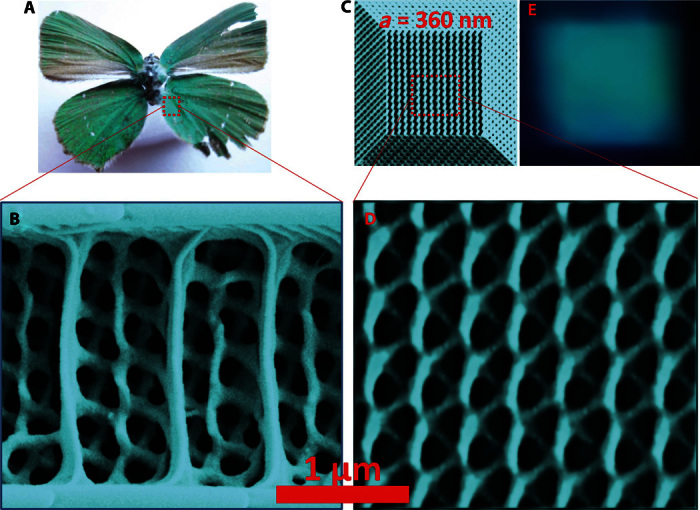
(A) Photograph of the butterfly C. rubi. (B) SEM image of the nanostructures found within the butterfly wings, with a periodicity of around 350 nm. (C) An artificial gyroid nanostructure fabricated by optical two-beam super-resolution lithography with a unit cell size of 360 nm. (D) Zoom-in of the artificial gyroid nanostructure. (E) White light reflection microscopy image of an artificial gyroid. Its lattice constant is 360 nm. The size of the structure is about 20 μm × 20 μm × 4 μm.
Here, we replicate the gyroid structure using an optical two-beam super-resolution lithography technique [the details of this technique, including material setup, can be found in Gan et al. (21)]. Figure 1 (C and D) shows a 3D gyroid nanostructure fabricated by optical two-beam super-resolution lithography with a lattice constant of 360 nm. These fabrication results demonstrate superior feature size, excellent feature resolution, long-range periodicity, and well-defined crystalline boundaries, proving the capability of this advanced technique to replicate natural photonic structures. With controllable structural handedness and excellent uniformity, these biomimetic nanostructures display both structural color, as found in C. rubi, and chiral properties lacking in the imperfect natural origin. In comparison with its natural origin, a white light reflection microscopy image of an artificial gyroid structure is shown in Fig. 1E. The artificial structure has a size of 20 μm × 20 μm × 4 μm, with a lattice constant of 360 nm. The blue-green color of the reflection image is similar to the visible color of the butterfly wings, demonstrating the high quality and high resolution of the fabricated artificial nanostructure.
Compared with conventional single-beam lithography technology (including two-photon polymerization), optical two-beam super-resolution lithography has two aspects that are of significant advantage: improved fabrication resolution and enhanced mechanical strength. Because optical two-beam super-resolution lithography requires a second beam, called the inhibition beam, to improve the fabrication resolution, its comparison to single-beam lithography is made with the inhibition beam off (Fig. 2A) and with the inhibition beam on (Fig. 2B).
Fig. 2. Comparison of 3D gyroid PCs fabricated by optical two-beam lithography with the inhibition beam off and with the inhibition beam on.
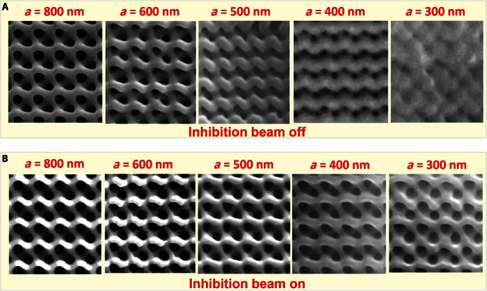
(A) The inhibition beam is off. (B) The inhibition beam is on.
Exceeding the resolution of nature
Using optical two-beam super-resolution lithography, we show that a unit cell size smaller than the natural origin can be made. Figure 2 shows the controllability of optical two-beam super-resolution lithography, compared with single-beam lithography, in fabricating gyroid structures with lattice constants from 800 to 300 nm. With the inhibition beam off, the structures are fabricated with a fabrication beam intensity of 75.75 mW/cm2 at a line scanning speed of 10 μm/s. The gyroid structures show excellent uniformity when their lattice constant is as large as 800 nm. However, at smaller size scales, the structures lose their geometrical constant as the fabricated features are no longer physically separated when the lattice constant is less than 400 nm. Thus, it is not possible to fabricate artificial gyroid structures with a lattice constant comparable to that found in the butterfly wings (350 nm) via single-beam lithography.
On the other hand, with the inhibition beam on (the intensity is 1.0 μW/cm2), super-resolution fabrication can be achieved and the gyroid structure can be scaled down to a lattice constant as small as 300 nm. When the lattice constant is 300 nm, the feature size is approximately 90 nm in the lateral direction. The filling ratio of the 300-nm lattice constant gyroid PC fabricated with the inhibition beam on was estimated to be 0.2. This result shows that the inhibition beam works well for improving fabrication resolution.
Superior mechanical strength via optical two-beam lithography
Compared with other technologies used to fabricate 3D structures, optical two-beam super-resolution lithography has the same advantage as the direct laser writing technique, that is, fabricating arbitrary structures (24–26). However, the material that is suitable for optical two-beam super-resolution lithography is limited to organic materials (21) at the current stage. Compared with inorganic materials, such as silicon (27) and metals (28–30), the material used in this work is comparatively softer. Thus, mechanical strength is an important issue in fabricating self-supported 3D structures.
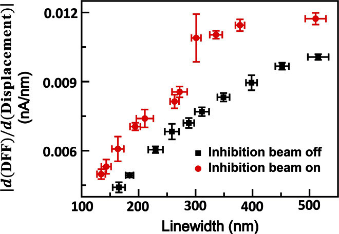
A careful comparison between Fig. 2A and Fig. 2B shows that the structures fabricated by optical two-beam super-resolution lithography have better mechanical strength as well. The structures presented in Fig. 2A fail to keep the standard srs network geometrical configuration because of significant structure collapse and distortion. When the fabricated feature size becomes smaller, the fabricated features are required to have sufficient mechanical strength to support each other as a 3D structure. When two-photon polymerization is used to fabricate a smaller-sized feature, a lower fabrication laser exposure dose is normally used. This process can reduce the monomer-to-polymer conversion rate (polymerization degree) and thus weaken the mechanical strength of the fabricated feature. However, optical two-beam super-resolution lithography can achieve a smaller feature through a mechanism different from that of general single-beam lithography, including two-photon polymerization. Rather than reducing the exposure dose of the laser beam–inducing polymerization, optical two-beam super-resolution lithography increases the exposure dose of the inhibition laser beam. As a result, the polymerization degree at the center of the laser focal spot does not decrease, and the steepness of the side slope for the polymerization degree curve becomes higher (section S1). This process increases the polymerization degree of the feature averaged over its size. Therefore, when two lines with the same linewidth are fabricated by two-photon polymerization and optical two-beam super-resolution lithography, the line fabricated by the latter method is expected to have higher mechanical strength. The experimental results presented in Fig. 3 prove this concept. Here, we measured mechanical strength property using atomic force microscopy (AFM), with experimental details presented in section S2. Figure 3 shows the mechanical strength property of lines [qualitatively characterized as |d(DFL)/d(Displacement)| in the “DFL (difference signal between top and bottom halves of the photodiode) signal”–displacement curve; see section S2] with different linewidths fabricated by optical two-beam super-resolution lithography with different fabrication beam exposure doses. In Fig. 3, the mechanical strength of a line becomes weaker if the linewidth becomes smaller for both fabrication methods. However, the mechanical strength is significantly better with optical two-beam lithography (inhibition beam on). The mechanical strength for a line with a linewidth of about 130 nm fabricated with the inhibition beam on is roughly equal to that of a line with a linewidth of about 185 nm fabricated with the inhibition beam off. Because of the enhanced mechanical strength, the artificial structure does not require the horizontal mechanical “struts” found within the natural counterpart, yet (see Fig. 1B) still has excellent mechanical stability.
Fig. 3. Mechanical properties of suspended lines fabricated by optical two-beam lithography with the inhibition beam on (red) and with the inhibition beam off (black).
Control of the overall shape of artificial gyroid nanostructures
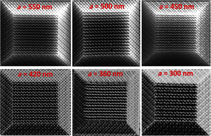
In many photonic applications, it is important to control the overall shape and orientation to allow for useful photonic functionality. Optical two-beam super-resolution lithography allows control of the overall shape with designed configuration and termination. Figure 4 shows large-scale artificial 3D gyroid PCs fabricated by optical two-beam super-resolution lithography for different lattice constants. These gyroid structures are designed to be pyramid-like in shape. Each of them has a size of 16 × 16 units in the top plane and a height of about 4 μm. All of these 3D structures are self-supported with sufficient mechanical strength, and thus can obtain good long-range uniformity. This is an essential property for applications such as chiral beam splitters (9). The fabricated structures show no obvious shrinkage or distortion. In contrast, the natural gyroid structures within butterfly wings are supported by struts to obtain sufficient mechanical strength. Figure 1A presents the structural distortion and nonuniformity observed within the natural nanostructures of the butterfly.
Fig. 4. Large-scale artificial gyroid PCs with different unit cell sizes showing good uniformity and mechanical strength.
Artificial gyroid structures with designable photonic property
Another important advantage of these artificial structures over their natural origin is their unique and designable photonic properties. The gyroid structure has been shown to have optical circular dichroism due to its chiral geometry. Light with right-handed circular polarization and light with left-handed circular polarization have different transmissions through gyroid PCs. However, the butterfly does not have this property because of the lack of structural uniformity (1, 13). The transmission spectra of two gyroid structures are measured and shown in Fig. 5. The results show the existence of a strong photonic bandgap and circular dichroism at visible wavelengths. The measured spectrum shows that the gyroid structure with a lattice constant of 360 nm displays a blue-green structural color, whereas it should roughly display a blue structural color when the lattice constant is 300 nm. This fits the observation presented in Fig. 1E and section S3. A number of gyroid structures with different lattice constants fabricated by varying inhibition beam intensities all show similar structural colors. When the lattice constant of the gyroid structure changes from 360 to 290 nm, the structural colors change from blue-green to blue (Fig. 5 and section S3). Although our fabrication technique can fabricate suspended lines with separations smaller than 100 nm (21), we did not successfully fabricate a high-quality gyroid structure with a lattice constant of 280 nm because a self-supported 3D structure needs to have enough mechanical strength. To scale down a gyroid structure to a lattice constant of 280 nm with clear structural component separation, we need a lower fabrication beam intensity or a higher inhibition beam intensity. This undoubtedly weakens the mechanical strength of the structure. We believe that the fabrication of a high-quality gyroid structure with a smaller lattice constant should be hindered for this reason. A numerical simulation of transmission spectra is also shown in Fig. 5. The excellent agreement between simulated and measured data demonstrates the accurate geometrical replication of the gyroid design. The simulation has a minor short-wavelength shift in the spectrum compared with the experiment. This may arise from the unexpected elongated axial direction feature size as a result of the repeated energy dosing of the inhibition beam for the experiment.
Fig. 5. Experimentally measured and simulated transmission spectra of gyroid structures fabricated by optical two-beam super-resolution lithography.
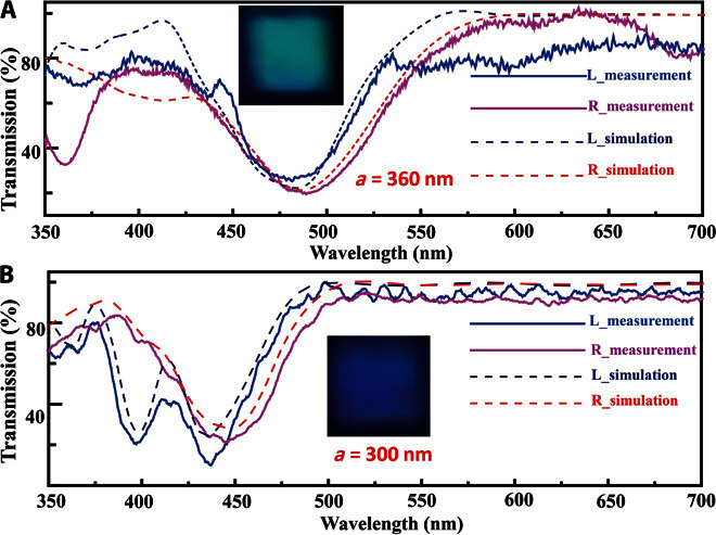
(A) The lattice constant of the gyroid structure is 360 nm. (B) The lattice constant of the gyroid structure is 300 nm. L, left; R, right.
DISCUSSION
We have demonstrated the replication of 3D biomimetic gyroid nanostructures at size scales smaller than their natural counterparts. The optical two-beam super-resolution lithography technique enables smaller unit cell sizes than nature. It offers more flexibility in structure design than nature, including unit cell size, filling fraction, and control of orientation and termination. It allows designable fabrication to demonstrate the applicable functionality. This work opens the door to the investigation of more gyroid-related applications in optics and photonics in the visible or near-ultraviolet wavelength region. It can also further enhance our understanding of these biological nanostructures and their functionality in nature.
MATERIALS AND METHODS
Materials and super-resolution lithography setup
Details of the photo resin used for optical two-beam super-resolution lithography (21) and the optical two-beam lithography setup (21) have been previously reported. The geometrical design of gyroid structures has been discussed in previous work (6, 9).
Measurement of mechanical strength property
The mechanical strength property of the fabricated features was characterized by nanoindentation (31–33) with an atomic force microscope (NT-MDT; NTEGRA Spectra). For a comparison of the mechanical strength of the suspended lines fabricated by optical two-beam super-resolution lithography with the inhibition beam on and with the inhibition beam off, the lines were fabricated with different fabrication beam intensities, whereas the inhibition beam was kept at 1.0 μW/cm2 while on. To ensure that the comparison was accurate, we measured all the DFL signal–displacement curve data by the same AFM tip. Here, we used |d(DFL)∕d(Displacement)| to qualitatively characterize the mechanical strength of the sample (section S2). Samples measured to have the same |d(DFL)∕d(Displacement)| value were regarded as having the same mechanical strength. The linewidths of the AFM-measured samples were finally measured with a ZEISS Supra 40VP field emission SEM system. When the measured suspended line has weak mechanical strength, the AFM measurement may break the line. Thus, the |d(DFL)∕d(Displacement)| data can be obtained only if the line is mechanically strong enough to survive after the AFM measurement.
Measurement of the transmission spectrum
Measurement of the transmission spectrum of gyroid structures was performed using a home-made setup. A white light beam traveling through a broadband half waveplate was focused by a 40× 0.65 NA (numerical aperture) objective lens. The fabricated artificial gyroid samples were aligned to the position where the focal spot of the white light beam could travel through the structure center at a normal incident angle. This allowed light to transmit through the [001] axis of gyroid structures. Before traveling through the structure, the white light beam was designed to travel through a broadband quarter waveplate. The transmitted light was collected by a 100× 0.8 NA objective lens and sent to a spectrograph to obtain the spectrum of the white light beam. The broadband quarter waveplate was rotated relative to the half waveplate to achieve a left- or right-handed circular polarization beam entering the structure. The transmission spectra shown in Fig. 5 were normalized by the measured white light beam spectrum with the sample removed.
Numerically simulated transmission spectrum
The simulation was completed with the commercial software CST Microwave Studio. The simulation used the gyroid (srs network) structure configuration with a line size of 90 nm in the lateral direction and a line size of 135 nm in the axial direction. The obtained data were smoothed for comparison with the experiment, where the finite angle of incidence of the focused light in the experimental data was taken into account.
Measurement of the reflection microscopy image
The fabricated artificial structure was loaded on a microscope. A white light beam was projected on the sample at an incident angle of about 10° corresponding to the artificial structure. The sample was placed on a slope at an angle of about 20°. The reflection microscopy image was taken by a charge-coupled device.
Supplementary Material
Acknowledgments
Funding: This work was supported in part by the Australian Research Council Centre for Ultrahigh-bandwidth Devices for Optical Systems (project number CE110001018) and by the Laureate Fellowship scheme (FL100100099). Z.G. was supported by the Science and Industry Endowment Fund under the John Stocker Postdoctoral Fellowship (project number PF14-100). Author contributions: Z.G. conceived and conducted the experiment and calculations, and analyzed the data. M.G. proposed the topic and supervised the project. All authors discussed the data and contributed to the writing of the paper. Competing interests: The authors declare that they have no competing interests. Data and materials availability: All data needed to evaluate the conclusions in the paper are presented in the paper and/or the Supplementary Materials. Additional data related to this paper may be requested from the authors.
SUPPLEMENTARY MATERIALS
Supplementary material for this article is available at http://advances.sciencemag.org/cgi/content/full/2/5/e1600084/DC1
S1. When optical single-beam lithography is used to fabricate a smaller-sized feature, a lower fabrication laser exposure dose is normally used.
S2. AFM characterization of mechanical property.
S3. White light reflection microscopy images of artificial gyroid structures.
fig. S1. Comparison of changes in polymerization degree between optical single-beam lithography and optical two-beam lithography to reduce the fabricated feature size.
fig. S2. AFM measurement of mechanical strength.
fig. S3. White light reflection microscopy images of artificial gyroid structures.
REFERENCES AND NOTES
- 1.Saba M., Wilts B. D., Hielscher J., Schröder-Turk G. E., Absence of circular polarisation in reflections of butterfly wing scales with chiral gyroid structure. Mater. Today 1, 193–208 (2014). [Google Scholar]
- 2.Mille C., Tyrode E. C., Corkery R. W., Inorganic chiral 3-D photonic crystals with bicontinuous gyroid structure replicated from butterfly wing scales. Chem. Commun. 47, 9873–9875 (2011). [DOI] [PubMed] [Google Scholar]
- 3.Saranathan V., Osuji C. O., Mochrie S. G. J., Noh H., Narayanan S., Sandy A., Dufresne E. R., Prum R. O., Structure, function, and self-assembly of single network gyroid (I4132) photonic crystals in butterfly wing scales. Proc. Natl. Acad. Sci. U.S.A. 107, 11676–11681 (2010). [DOI] [PMC free article] [PubMed] [Google Scholar]
- 4.Michielsen K., Stavenga D. G., Gyroid cuticular structures in butterfly wing scales: Biological photonic crystals. J. R. Soc. Interface 5, 85–94 (2008). [DOI] [PMC free article] [PubMed] [Google Scholar]
- 5.Dolan J. A., Wilts B. D., Vijgnolini S., Baumberg J. J., Steiner U., Wilkinson T. D., Optical properties of gyroid structured materials: From photonic crystals to metamaterials. Adv. Opt. Mater. 3, 12–32 (2015). [Google Scholar]
- 6.Turner M. D., Schröder-Turk G. E., Gu M., Fabrication and characterization of three-dimensional biomimetic chiral composites. Opt. Express 19, 10001–10008 (2011). [DOI] [PubMed] [Google Scholar]
- 7.Oh S. S., Demetriadou A., Wuestner S., Hess O., On the origin of chirality in nanoplasmonic gyroid metamaterials. Adv. Mater. 25, 612–617 (2013). [DOI] [PubMed] [Google Scholar]
- 8.Hyde S. T., Schröder-Turk G. E., Geometry of interfaces: Topological complexity in biology and materials. Interface Focus 2, 529–538 (2012). [Google Scholar]
- 9.Turner M. D., Saba M., Zhang Q., Cumming B. P., Schröder-Turk G. E., Gu M., Miniature chiral beamsplitter based on gyroid photonic crystals. Nat. Photonics 7, 801–805 (2013). [Google Scholar]
- 10.Lu L., Fu L., Joannopoulos J. D., Soljačić M., Weyl points and line nodes in gyroid photonic crystals. Nat. Photonics 7, 294–299 (2013). [Google Scholar]
- 11.Farah P., Demetriadou A., Salvatore S., Vignolini S., Stefik M., Wiesner U., Hess O., Steiner U., Valev V. K., Baumberg J. J., Ultrafast nonlinear response of gold gyroid three-dimensional metamaterials. Phys. Rev. Appl. 2, 044002 (2014). [Google Scholar]
- 12.Cumming B. P., Turner M. D., Schröder-Turk G. E., Debbarma S., Luther-Davies B., Gu M., Adaptive optics enhanced direct laser writing of high refractive index gyroid photonic crystals in chalcogenide glass. Opt. Express 22, 689–698 (2014). [DOI] [PubMed] [Google Scholar]
- 13.Poladian L., Wickham S., Lee K., Large M. C. J., Iridescence from photonic crystals and its suppression in butterfly scales. J. R. Soc. Interface 6 (Suppl. 2), S233–S242 (2009). [DOI] [PMC free article] [PubMed] [Google Scholar]
- 14.Blanco A., Chomski E., Grabtchak S., Ibisate M., John S., Leonard S. W., Lopez C., Meseguer F., Miguez H., Mondia J. P., Ozin G. A., Toader O., van Driel H. M., Large-scale synthesis of a silicon photonic crystal with a complete three-dimensional bandgap near 1.5 micrometres. Nature 405, 437–440 (2000). [DOI] [PubMed] [Google Scholar]
- 15.Ullal C. K., Maldovan M., Thomas E. L., Chen G., Han Y.-J., Yang S., Photonic crystals through holographic lithography: Simple cubic, diamond-like, and gyroid-like structures. Appl. Phys. Lett. 84, 5434–5436 (2004). [Google Scholar]
- 16.Vlasov Y. A., Bo X.-Z., Sturm J. C., Norris D. J., On-chip natural assembly of silicon photonic bandgap crystals. Nature 414, 289–293 (2001). [DOI] [PubMed] [Google Scholar]
- 17.Vogelaar L., Nijdam W., van Wolferen H. A. G. M., de Ridder R. M., Segerink F. B., Flück E., Kuipers L., van Hulst N. F., Large area photonic crystal slabs for visible light with waveguiding defect structures: Fabrication with focused ion beam assisted laser interference lithography. Adv. Mater. 13, 1551–1554 (2001). [Google Scholar]
- 18.Lu L., Wang Z., Ye D., Ran L., Fu L., Joannopoulos J. D., Soljačić M., Experimental observation of Weyl points. Science 349, 622–624 (2015). [DOI] [PubMed] [Google Scholar]
- 19.P. Rai-Choudhury, Handbook of Microlithography, Micromachining, and Microfabrication (SPIE Optical Engineering Press, Bellingham, WA, 1997), 692 pp. [Google Scholar]
- 20.Pan L., Park Y., Xiong Y., Ulin-Avila E., Wang Y., Zeng L., Xiong S., Rho J., Sun C., Bogy D. B., Zhang X., Maskless plasmonic lithography at 22 nm resolution. Sci. Rep. 1, 175 (2011). [DOI] [PMC free article] [PubMed] [Google Scholar]
- 21.Gan Z., Cao Y., Evans R. A., Gu M., Three-dimensional deep sub-diffraction optical beam lithography with 9 nm feature size. Nat. Commun. 4, 2061 (2013). [DOI] [PubMed] [Google Scholar]
- 22.Gan Z., Cao Y., Jia B., Gu M., Dynamic modeling of superresolution photoinduced-inhibition nanolithography. Opt. Express 20, 16871–16879 (2012). [Google Scholar]
- 23.Saba M., Thiel M., Turner M. D., Hyde S. T., Gu M., Grosse-Brauckmann K., Neshev D. N., Mecke K., Schröder-Turk G. E., Circular dichroism in biological photonic crystals and cubic chiral nets. Phys. Rev. Lett. 106, 103902 (2011). [DOI] [PubMed] [Google Scholar]
- 24.Gan Z., Jia B., Liu J.-F., Wang X.-H., Gu M., Enhancement of spontaneous emission in three-dimensional low refractive-index photonic crystals with designed defects. Appl. Phys. Lett. 101, 071109 (2012). [Google Scholar]
- 25.Nicoletti E., Bulla D., Luther-Davies B., Gu M., Planar defects in three-dimensional chalcogenide glass photonic crystals. Opt. Lett. 36, 2248–2250 (2011). [DOI] [PubMed] [Google Scholar]
- 26.Deubel M., Wegener M., Linden S., von Freymann G., John S., 3D–2D–3D photonic crystal heterostructures fabricated by direct laser writing. Opt. Lett. 31, 805–807 (2006). [DOI] [PubMed] [Google Scholar]
- 27.Lin S. Y., Fleming J. G., Hetherington D. L., Smith B. K., Biswas R., Ho K. M., Sigalas M. M., Zubrzycki W., Kurtz S. R., Bur J., A three-dimensional photonic crystal operating at infrared wavelengths. Nature 394, 251–253 (1998). [Google Scholar]
- 28.De Angelis F., Liberale C., Coluccio M. L., Cojoc G., Di Fabrizio E., Emerging fabrication techniques for 3D nano-structuring in plasmonics and single molecule studies. Nanoscale 3, 2689–2696 (2011). [DOI] [PubMed] [Google Scholar]
- 29.Romanato F., Businaro L., Vaccari L., Cabrini S., Candeloro P., De Vittorio M., Passaseo A., Todaro M. T., Cingolani R., Cattaruzza E., Galli M., Andreani C., Di Fabrizio E., Fabrication of 3D metallic photonic crystals by X-ray lithography. Microelectron. Eng. 67–68, 479–486 (2003). [Google Scholar]
- 30.Romanato F., Tormen M., Businaro L., Vaccari L., Stomeo T., Passaseo A., Di Fabrizio E., X-ray lithography for 3D microfluidic applications. Microelectron. Eng. 73–74, 870–875 (2004). [Google Scholar]
- 31.Krake B., Damaschke B., Measurement of nanohardness and nanoelasticity of thin gold films with scanning force microscope. Appl. Phys. Lett. 77, 361–363 (2000). [Google Scholar]
- 32.Domke J., Radmacher M., Measuring the elastic properties of thin polymer films with the atomic force microscope. Langmuir 14, 3320–3325 (1998). [Google Scholar]
- 33.Ko F., Gogotsi Y., Ali A., Naguib N., Ye H., Yang G. L., Li C., Willis P., Electrospinning of continuous carbon nanotube-filled nanofiber yarns. Adv. Mater. 15, 1161–1165 (2003). [Google Scholar]
Associated Data
This section collects any data citations, data availability statements, or supplementary materials included in this article.
Supplementary Materials
Supplementary material for this article is available at http://advances.sciencemag.org/cgi/content/full/2/5/e1600084/DC1
S1. When optical single-beam lithography is used to fabricate a smaller-sized feature, a lower fabrication laser exposure dose is normally used.
S2. AFM characterization of mechanical property.
S3. White light reflection microscopy images of artificial gyroid structures.
fig. S1. Comparison of changes in polymerization degree between optical single-beam lithography and optical two-beam lithography to reduce the fabricated feature size.
fig. S2. AFM measurement of mechanical strength.
fig. S3. White light reflection microscopy images of artificial gyroid structures.


