Abstract
Layered two-dimensional semiconductors have attracted tremendous attention owing to their demonstrated excellent transistor switching characteristics with a large ratio of on-state to off-state current, Ion/Ioff. However, the depletion-mode nature of the transistors sets a limit on the thickness of the layered semiconductor films primarily determined by a given Ion/Ioff as an acceptable specification. Identifying the optimum thickness range is of significance for material synthesis and device fabrication. Here, we systematically investigate the thickness-dependent switching behavior of transistors with a wide thickness range of multilayer-MoS2 films. A difference in Ion/Ioff by several orders of magnitude is observed when the film thickness, t, approaches a critical depletion width. The decrease in Ion/Ioff is exponential for t between 20 nm and 100 nm, by a factor of 10 for each additional 10 nm. For t larger than 100 nm, Ion/Ioff approaches unity. Simulation using technical computer-aided tools established for silicon technology faithfully reproduces the experimentally determined scaling behavior of Ion/Ioff with t. This excellent agreement confirms that multilayer-MoS2 films can be approximated as a homogeneous semiconductor with high surface conductivity that tends to deteriorate Ion/Ioff. Our findings are helpful in guiding material synthesis and designing advanced field-effect transistors based on the layered semiconductors.
The first successful demonstration of field-effect transistors (FETs) based on monolayer molybdenum disulfide (MoS2) with appealing performance1,2 has stimulated intensive research on two-dimensional (2D) transition metal dichalcogenides (TMDs). The planar nature of these 2D semiconductor materials could potentially lead complementary metal-oxide-semiconductor (CMOS) technology to the ultimate size scaling envisioned by Moore’s law and beyond3,4,5. MoS2, a representative layered TMD, has a satisfactory bandgap in the range of 1.3 to 1.8 eV6,7, which is advantageous over the well-studied gapless graphene with respect to the standby leakage current of its FETs8. The bandgap of MoS2 is thickness-dependent and it is 1.8 eV for monolayers. As a result, transistors of both single- and multilayer-MoS2 films have an exhibited high ratio of on-state to off-state current (Ion/Ioff > 106) with reasonable electron mobility1,9,10,11. All this makes the layered TMDs promising in fields of low-power switches/circuits11,12, nonvolatile memory devices13,14, ultrasensitive photodetectors15,16, etc.
In FET applications, multilayer MoS2 with a smaller bandgap is of greater potential than the monolayer counterpart17. First, multilayer MoS2 has a 3-fold higher density of states and conducts current along multiple channels, which can be translated to a considerably high drive current11,18. Second, the interlayer screening effect leads to a higher carrier mobility19,20 and better noise immunity21 in multilayer MoS2. Compared to the direct-bandgap monolayer MoS2 requiring a strict thickness control, the electronic properties of multilayer MoS2 manifested by an indirect bandgap are relatively insensitive to layer thickness. Hence, multilayer MoS2 is better suited for large-area and/or high-density electronics22,23,24. However, multilayer MoS2 and other TMD semiconductors have so far gained limited attention for their use in electronics, compared to their monolayer counterparts.
Usually, MoS2 is an n-type semiconductor that is determined by both intrinsic and extrinsic effects, such as sulfur vacancies, impurities or other structural defects25,26,27. Control of the electron mobility and carrier density in MoS2 FETs can be achieved by engineering on the gate structure and dielectrics28,29,30. In multilayer MoS2, the gate control of the electron density in the channel is weakened with increasing MoS2 thickness. When the MoS2 thickness is larger than the maximum depletion width, Wmax, the electrostatic gating loses control over the electrons in the excess part of the MoS2 film beyond Wmax. This situation is well known in the partially depleted silicon-on-insulator (SOI) technology. If there is no energy barrier at the source or drain terminals, the electrons in this excess MoS2 will contribute significantly to the leakage current. The potential advantages of multilayer MoS2 are, then, offset by a high Ioff, leading to a significantly reduced Ion/Ioff. Hence, identifying the optimum thickness range is of significance for material synthesis and practical device application of the 2D TMDs. For digital logic applications, Ion/Ioff of at least 103 is generally required31. In this work, we will use this Ion/Ioff = 103 ratio as a design criterion, especially when an optimum layer thickness is concerned for achieving high performance with acceptable Ion/Ioff. In view of performance variation associated with probable non-uniformity with unintentional n-doping in the starting MoS2 material as well as from device fabrication, this work builds on a statistical study of the key device parameters in order to gain a comprehensive understanding of the switching properties. Specifically, we investigate the thickness-dependent Ion/Ioff in multilayer MoS2 by a statistical analysis of more than 80 devices in a wide thickness range. Differences in Ion/Ioff are large amounting to several orders of magnitude with increasing layer thickness. The optimum layer thickness is defined by Wmax, beyond which Ion/Ioff is reduced below 103.
Results
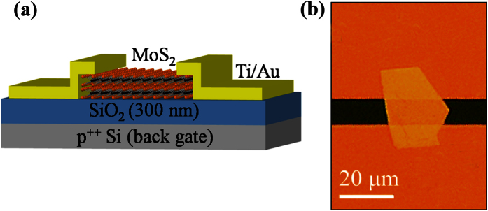
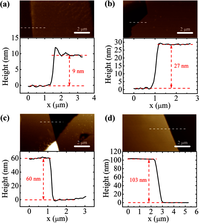
A schematic representation of a back-gate multilayer-MoS2 transistor used in our work is shown in Fig. 1a, whereas a typical top view photomicrograph of a fabricated device is given in Fig. 1b. Isolated MoS2 flakes on the SiO2/Si substrate were exfoliated from a bulk MoS2 crystal using a conventional mechanical exfoliation technique32. The sample preparation and device fabrication are detailed in Methods. The thickness of different flakes, t, was measured by means of atomic force microscopy (AFM), as illustrated in Fig. 2. Only one channel length of 10 μm is used for all devices and it is defined by the spacing of a Cu grid shadow mask. However, the channel width that is determined by the width of the flakes varies in the range of 2–60 μm as a result of the stochastic nature of the MoS2 exfoliation process. The source and drain metal used in our devices is 50 nm Au with a 5 nm thick Ti adhesion layer. The Ti adhesion layer that is in intimate contact with MoS2 has a work function of ∼4.3 eV, which is very close to the conduction band edge of thin-layer MoS29,33. Furthermore, Ti is a transition metal with its d-electron orbitals mixing favorably with the 4d states of Mo and resulting in an increase in the density of states at the Fermi level and a strong Fermi level pinning at the contact9,34,35. Therefore, this favorable interface geometry is expected to facilitate a good chemical bonding and allow for a maximized electron injection at the source/drain contacts with an increased overlap between the states at the interface.
Figure 1.
(a) Schematic representation and (b) Optical image of the field-effect transistor based on multilayer MoS2.
Figure 2.
(a–d) AFM images of 9, 27, 60 and 103-nm thick MoS2 films on SiO2/Si substrate. The height profiles are measured along the dashed lines in the images.
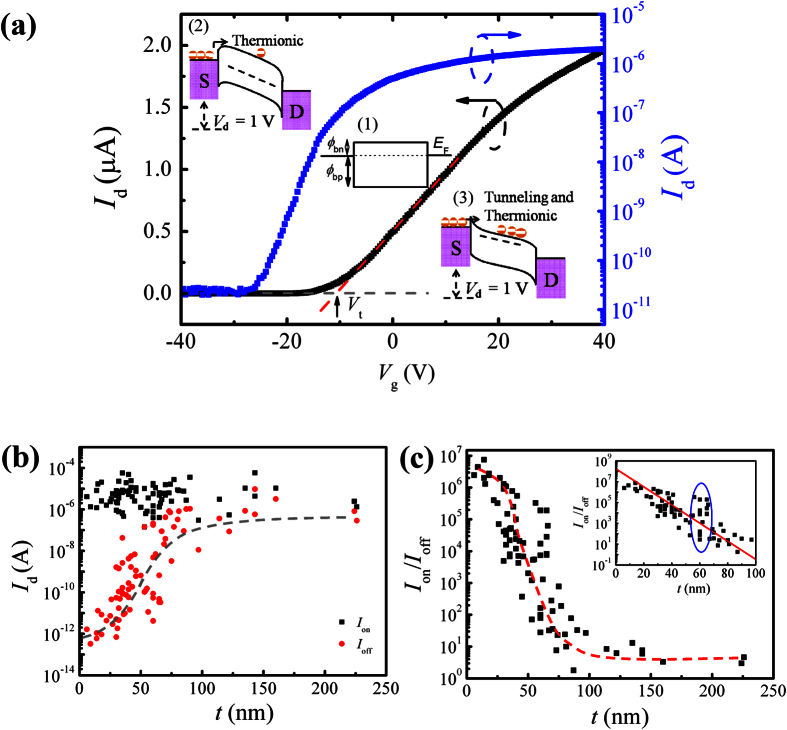
The transfer characteristics of a multilayer-MoS2 FET shows a typical n-type unipolar carrier transport behavior (Fig. 3a). This confirms a rather small (<0.1 eV), if not negligible, Schottky barrier height (SBH) for electrons at the Au/Ti-MoS2 contacts (Supplementary Fig. S1). The SBH for holes is, thus, high (>1.2 eV) since the sum of electron SBH and hole SBH should approximately be equal to the energy bandgap (1.3 eV) of MoS2 (inset in Fig. 3a). Tunneling through the Schottky barrier at the metal/MoS2 contacts not only limits the charge injection in the device at its on-state but also plays a critical role when evaluating the device off-state in the subthreshold region of the transistor. The small electron SBH facilitates the injection of accumulated electrons at positive gate voltage, Vg, while the large hole SBH suppresses the injection of inverted holes at negative Vg. This results in the n-type unipolar behavior with a high Ion/Ioff and is in stark contrast to the ambipolar conduction behavior in graphene FETs with a low Ion/Ioff32. The FET with a 30-nm-thick multilayer MoS2 in Fig. 3a operates as a depletion-mode FET with a large negative threshold voltage, Vt, and a high Ion/Ioff of 105. All the FETs fabricated in this work exhibit the same n-type characteristics, regardless of the thickness of the MoS2 film in channel (Supplementary Fig. S2).
Figure 3.
(a) Transfer characteristics of a representative transistor with a 30-nm-thick MoS2 film on a linear scale (left y-axis) and a log scale (right y-axis). The threshold voltage, Vt, is determined by the intercept on the x-axis with the regression fitted line to the linear scale characteristics. The insets represent the energy band diagrams corresponding to the applied Vg in three distinct regions: (1) at flat band, (2) below threshold, and (3) above threshold. ϕbn and ϕbp indicate electron and hole SBH, respectively. (b) Dependence of Ion and Ioff on MoS2 flake thickness. The grey dashed line serves as a guide to the eye. (c) Thickness-dependence of Ion/Ioff. The red dashed line serves as a guide to the eye. Inset is the zoom in for the first 100 nm. The red solid line in the inset is a linear fit on the semi-log scale.
The depletion-mode nature of the transistors will set a limit on the thickness of the multilayer MoS2 films primarily determined by the preset Ion/Ioff = 103 as an acceptable specification. Over 80 multilayer-MoS2 FETs were fabricated and characterized. Their Ion and Ioff versus t ranging from 6 nm to 225 nm are plotted in Fig. 3b. The minimum Ioff occurring for the smallest t is limited by the noise level in the devices. A clear trend is observed for Ioff; it increases rapidly with increasing t below 100 nm. Beyond t = 100 nm, Ioff becomes comparable with Ion and is almost independent of layer thickness. The stochastic variation of the flake widths makes the variation of Ion with t unspecific. However, Ion/Ioff is unaffected by the width variation due to the same width-dependence of Ion and Ioff36. In the first 20–30 nm, Ion/Ioff exhibits a gradual decrease with increasing t, see Fig. 3c, likely caused by the Ioff variation. This is followed by an exponential decrease in Ion/Ioff with t until it approaches unity for t > 100 nm. This is better seen in the inset of Fig. 3c where the best linear fit to the logarithmic Ion/Ioff versus t in the range of 20–100 nm gives
 |
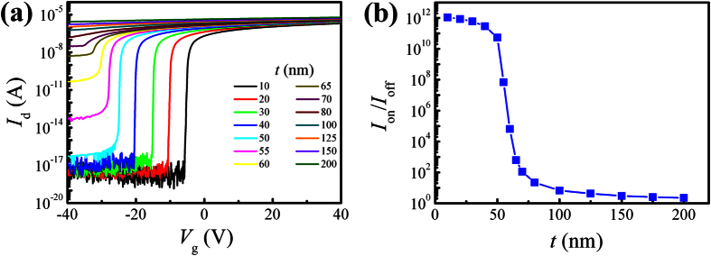
It is well known that in the monolayer 2D materials, the charge carriers are confined in the 2D planes. This confinement can result in some unique characteristics not common in 3D materials, e.g. Si. When the layer thickness is increased, the carriers can hop freely between neighboring layers and move in the whole 2D layered material37. As a result, the carriers distribute fairly uniformly in the 2D material. In this aspect, multilayer-MoS2 films can be approximated as a homogeneous semiconductor and simulated with traditional device simulators. We have therefore used a commercial simulation tool SILVACO TCAD38 to numerically solve the coupled Poisson and continuity equations for the multilayer-MoS2 FETs. Our focus here is on charge and current distributions in MoS2. For simplicity, the electron SBH is set to 0.1 eV and the unintentional n-doping concentration, Nd, in MoS2 is assumed to be 3.5 × 1017 cm−3, in order to attain identical Vt between the simulation and experiments. The doping concentration39 in MoS2 is found to vary from 1016 to 1019 cm−3. The other material parameters used in the simulation are shown in Supplementary Table S111,39,40. The simulated transfer characteristics of multilayer-MoS2 FETs for various channel thicknesses (Fig. 4a) and the variation of Ion/Ioff with t (Fig. 4b) are in good agreement with the experimental results. In particular, the simulated Ion/Ioff shows a steep decrease with t around ~50 nm, matching very well with the data in Fig. 3c. This critical thickness is strongly correlated with Wmax that is related to Nd by the following formula36:
Figure 4.
(a) Simulated transfer curves of FETs with various MoS2 thicknesses. (b) Simulated thickness-dependence of Ion/Ioff.
 |
where, k is the Boltzmann constant, T is absolute temperature, q is elementary charge, εs is the relative dielectric constant of multilayer MoS2 (~11)39,41, ε0 is the vacuum permittivity, and ni = 1.6 × 108 cm−3 is the intrinsic carrier concentration in MoS2 due to thermal interband excitation11. The calculated Wmax with the given Nd is ~60 nm. The spatial distribution of charge carriers is inhomogeneous, due to charge screening, along the depth of the multilayer-MoS2 film. Specifically, the charge carriers in the MoS2 layers close to the SiO2 interface are effectively controlled by Vg. The electrostatic gate control of the carriers are weakened gradually, or even completely lost, in the MoS2 layers further away from the SiO2 interface on the account of charge screening.
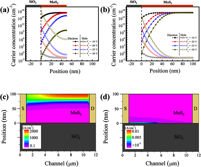
As the device switching behavior is mainly determined by Ioff, the carrier distribution at negative Vg is shown, respectively, in Fig. 5a,b for t < Wmax and t > Wmax. At a negative Vg, electrons are repelled from while holes are attracted to the MoS2/SiO2 interface. For t < Wmax, electrons are depleted in the whole MoS2 film at Vg < −25 V. Simultaneously, an inversion layer populated with holes is formed at the MoS2/SiO2 interface. However, when t > Wmax, the carrier concentration close to the sample surface (away from the MoS2/SiO2 interface) remains constant independent of Vg. This is a result of charge screening effect that results in a poor electrostatic control of the electrons in the excess part of the MoS2 film. This high and uncontrolled electron concentration in this excess MoS2 close to the sample surface, shown in Fig. 5c, contributes to Ioff. Although a hole inversion layer is formed under large negative Vg, the hole conduction current can be neglected due to a large SBH at the contact interfaces (see Fig. 5d).
Figure 5.
Carrier distribution in 50-nm (a) and 100-nm (b) MoS2 at various Vg. (c,d) Electron and hole current distributions in a 100-nm-thick MoS2 at Vg = −30 V.
It is established now that Wmax is an important parameter determining the switching behavior of multilayer-MoS2 FETs. When t ≪ Wmax, the electrons can be fully depleted from the entire channel region under negative Vg and an excellent switching behavior with a very low leakage current prevails. Under such circumstances, Ion/Ioff is rather insensitive to t, as manifested by the slowly descending Ion/Ioff with t shown in Figs 3c and 4b. When t around Wmax, the electrons in the excess part of the MoS2 film cannot be fully depleted easily. An exponential decrease in Ion/Ioff by about 4 orders of magnitude with t changing from 30 to 65 nm. Moreover, Wmax depends on doping concentration. The stochastic doping concentration in the MoS2 flakes can induce a variation in Wmax, which in its turn results in a large spread in the switching property at ~60 nm (indicated by a circle in the inset of Fig. 3c).
Discussion
In view of its significance in device physics, design and fabrication, quantifying the transistor switching behavior as a function of the layer thickness of the 2D semiconductor materials is of vital importance. A critical parameter Wmax is discussed when characterizing layered TMD semiconductors such as MoS2 as the channel material in FETs. Both experimental and theoretical studies show Wmax = 50–60 nm for the multilayer-MoS2 FETs. At this thickness, the FETs are characterized by an acceptable Ion/Ioff around 103. If the multilayer-MoS2 film is thinner than this Wmax, an excellent switching behavior with a low leakage current and a much higher Ion/Ioff (than 103) will prevail. If the multilayer-MoS2 film is substantially thicker than this Wmax, a large leakage current will persist and the switching behavior becomes inferior. An exponential decrease in Ion/Ioff is found in the 20–100 nm thickness range, by a factor of 10 for each additional 10 nm. The findings in this work are useful in guiding material synthesis and designing advanced FETs with layered TMD semiconductors. It appears that the device physics established for traditional semiconductors such as Si is applicable for the layered TMD semiconductors, as it should be.
Methods
Thin MoS2 flakes were peeled off from bulk MoS2 (SPI supplies) by mechanical exfoliation. They were subsequently transferred to a heavily doped p-type Si substrate with a 300-nm-thick thermally grown SiO2. The SiO2/Si substrate was pre-cleaned by sonication in acetone, isopropyl alcohol, and deionized water. The transferred MoS2 flakes were identified using an optical microscope (Keyence digital microscope VHX-600). The thickness of the MoS2 flakes was measured using AFM (Dimension 3100 with Nanoscope IIIa controller, Veeco) operated in tapping mode under ambient conditions. In order to avoid contamination from photolithography or electron-beam lithography, a 10-μm spacing copper grid was placed on top of the thin MoS2 flakes as a shadow mask for the electrode fabrication. A bilayer stack Ti/Au of 5/50 nm thickness was then deposited by means of electron-beam evaporation as the source and drain electrodes. The heavily doped Si substrate was used as the common back gate for the fabricated MoS2 FETs. Electrical characterization of the devices was carried out in a shielded probe station with Keithley 4200 semiconductor characterization system in ambient environments.
Additional Information
How to cite this article: Zhang, Y. et al. Thickness Considerations of Two-Dimensional Layered Semiconductors for Transistor Applications. Sci. Rep. 6, 29615; doi: 10.1038/srep29615 (2016).
Supplementary Material
Acknowledgments
This work is supported partially by the National Natural Science Foundation of China (Nos 61204090 and 61171010), Fundamental Research Project of young teachers to enhance research capacity, Fudan University (No. 20520133248), State Key Laboratory of ASIC & System, Fudan University (No. 2015MS005), the Swedish Research Council (No. 2014-5591) and the Knut & Alice Wallenberg Foundation (No. 2011.0082).
Footnotes
The authors declare no competing financial interests.
Author Contributions Z.-J.Q. conceived the research and analyzed the results. Y.Z., H.W. and H.X. carried out MoS2 device fabrication. Y.Z. performed AFM analysis and electrical characterization. H.L. performed TCAD simulation. Z.-J.Q., S.-L.Z. and R.L. wrote the manuscript. All authors discussed the results and commented the manuscript.
References
- Radisavljevic B., Radenovic A., Brivio J., Giacometti V. & Kis A. Single-layer MoS2 transistors. Nature Nanotechnol. 6, 147–150 (2011). [DOI] [PubMed] [Google Scholar]
- Wang Q. H., Kalantar-Zadeh K., Kis A., Coleman J. N. & Strano M. S. Electronics and optoelectronics of two-dimensional transition metal dichalcogenides. Nature Nanotechnol. 7, 699–712 (2012). [DOI] [PubMed] [Google Scholar]
- Liu L., Kumar S. B., Ouyang Y. & Guo J. Performance limits of monolayer transition metal dichalcogenide transistors. IEEE Trans. Electron Devices 58, 3042–3047 (2011). [Google Scholar]
- Yoon Y., Ganapathi K. & Salahuddin S. How good can monolayer MoS2 transistors be? Nano Lett. 11, 3768–3773 (2011). [DOI] [PubMed] [Google Scholar]
- Alam K. & Lake R. K. Monolayer MoS2 transistors beyond the technology road map. IEEE Trans. Electron Devices 59, 3250–3254 (2012). [Google Scholar]
- Mak K. F., Lee C., Hone J., Shan J. & Heinz T. F. Atomically thin MoS2: a new direct-gap semiconductor. Phys. Rev. Lett. 105, 136805 (2010). [DOI] [PubMed] [Google Scholar]
- Splendiani A. et al. Emerging photoluminescence in monolayer MoS2. Nano Lett. 10, 1271–1275 (2010). [DOI] [PubMed] [Google Scholar]
- Schwierz F. Graphene transistors. Nature Nanotechnol. 5, 487–496 (2010). [DOI] [PubMed] [Google Scholar]
- Das S., Chen H.-Y., Penumatcha A. V. & Appenzeller J. High performance multilayer MoS2 transistors with scandium contacts. Nano Lett. 13, 100–105 (2013). [DOI] [PubMed] [Google Scholar]
- Liu H., Neal A. T. & Ye P. D. Channel length scaling of MoS2 MOSFETs. ACS Nano 6, 8563–8569 (2012). [DOI] [PubMed] [Google Scholar]
- Kim S. et al. High-mobility and low-power thin-film transistors based on multilayer MoS2 crystals. Nature Commun. 3, 1011 (2012). [DOI] [PubMed] [Google Scholar]
- Chang H.-Y. et al. High-performance, highly bendable MoS2 transistors with high-K dielectrics for flexible low-power systems. ACS Nano 7, 5446–5452 (2013). [DOI] [PubMed] [Google Scholar]
- Bertolazzi S., Krasnozhon D. & Kis A. Nonvolatile memory cells based on MoS2/graphene heterostructures. ACS Nano 7, 3246–3252 (2013). [DOI] [PubMed] [Google Scholar]
- Lee H. S. et al. MoS2 Nanosheets for top-gate nonvolatile memory transistor channel. Small 8, 3111–3115 (2012). [DOI] [PubMed] [Google Scholar]
- Lopez-Sanchez O., Lembke D., Kayci M., Radenovic A. & Kis A. Ultrasensitive photodetectors based on monolayer MoS2. Nature Nanotechnol. 8, 497–501 (2013). [DOI] [PubMed] [Google Scholar]
- Choi W. et al. High-detectivity multilayer MoS2 phototransistors with spectral response from ultraviolet to infrared. Adv. Mater. 24, 5832–5836 (2012). [DOI] [PubMed] [Google Scholar]
- Ganatra R. & Zhang Q. Few-layer MoS2: A promising layered semiconductor. ACS Nano 8, 4074–4099 (2014). [DOI] [PubMed] [Google Scholar]
- Kaasbjerg K., Thygesen K. S. & Jacobsen K. W. Phonon-limited mobility in n-type single-layer MoS2 from first principles. Phys. Rev. B 85, 115317 (2012). [Google Scholar]
- Castellanos-Gomez A. et al. Electric-field screening in atomically thin layers of MoS2: the role of interlayer coupling. Adv. Mater. 25, 899–903 (2013). [DOI] [PubMed] [Google Scholar]
- Li S.-L. et al. Thickness-dependent interfacial coulomb scattering in atomically thin field-effect transistors. Nano Lett. 13, 3546–3552 (2013). [DOI] [PubMed] [Google Scholar]
- Kwon H.-J., Kang H., Jang J., Kim S. & Grigoropoulos C. P. Analysis of flicker noise in two-dimensional multilayer MoS2 transistors. Appl. Phys. Lett. 104, 083110 (2014). [Google Scholar]
- Liu K.-K. et al. Growth of large-area and highly crystalline MoS2 thin layers on insulating substrates. Nano Lett. 12, 1538–1544 (2012). [DOI] [PubMed] [Google Scholar]
- Laskar M. R. et al. Large area single crystal (0001) oriented MoS2. Appl. Phys. Lett. 102, 252108 (2013). [Google Scholar]
- Tarasov A. et al. Highly uniform trilayer molybdenum disulfide for wafer-scale device fabrication. Adv. Funct. Mater. 24, 6389–6400 (2014). [Google Scholar]
- Qiu H. et al. Hopping transport through defect-induced localized states in molybdenum disulphide. Nature Commun. 4, 2642 (2013). [DOI] [PubMed] [Google Scholar]
- Zhou W. et al. Intrinsic structural defects in monolayer molybdenum disulfide. Nano Lett. 13, 2615–2622 (2013). [DOI] [PubMed] [Google Scholar]
- Najmaei S., Yuan J., Zhang J., Ajayan P. & Lou J. Synthesis and defect investigation of two-dimensional molybdenum disulfide atomic layers. Acc. Chem. Res. 48, 31–40 (2015). [DOI] [PubMed] [Google Scholar]
- Radisavljevic B. & Kis A. Mobility engineering and a metal-insulator transition in monolayer MoS2. Nature Mater. 12, 815–820 (2013). [DOI] [PubMed] [Google Scholar]
- Zou X. et al. Interface engineering for high-performance top-gated MoS2 field-effect transistors. Adv. Mater. 26, 6255–6261 (2014). [DOI] [PubMed] [Google Scholar]
- Zhang Y., Ye J., Matsuhashi Y. & Iwasa Y. Ambipolar MoS2 thin flake transistors. Nano Lett. 12, 1136–1140 (2012). [DOI] [PubMed] [Google Scholar]
- Jariwala D., Sangwan V. K., Lauhon L. J., Marks T. J. & Hersam M. C. Emerging device applications for semiconducting two-dimensional transition metal dichalcogenides. ACS Nano 8, 1102–1120 (2014). [DOI] [PubMed] [Google Scholar]
- Novoselov K. S. et al. Electric field effect in atomically thin carbon films. Science 306, 666–669 (2004). [DOI] [PubMed] [Google Scholar]
- Hughes H. P. & Starnberg H. I. Electron Spectroscopies Applied to Low-Dimensional Structures. Kluwer Academic Publishers: Dordrecht, the Netherlands, 2000). [Google Scholar]
- Popov I., Seifert G. & Tománek D. Designing electrical contacts to MoS2 monolayers: a computational study. Phys. Rev. Lett. 108, 156802 (2012). [DOI] [PubMed] [Google Scholar]
- Gong C., Colombo L., Wallace R. M. & Cho K. The unusual mechanism of partial Fermi level pinning at metal-MoS2 interfaces. Nano Lett. 14, 1714–1720 (2014). [DOI] [PubMed] [Google Scholar]
- Taur Y. & Ning T. H. Fundamentals of Modern VLSI Devices, (Cambridge University Press: Cambridge, UK 1998). [Google Scholar]
- Zhang Y. et al. On Valence-band splitting in layered MoS2. ACS Nano 9, 8514–8519 (2015). [DOI] [PubMed] [Google Scholar]
- SILVACO. ATLAS User’s Manual. SILVACO Inc., Santa Clara, CA 95054, 2008.
- Howell S. L. et al. Investigation of band-offsets at monolayer-multilayer MoS2 junctions by scanning photocurrent microscopy. Nano Lett. 15, 2278–2284 (2015). [DOI] [PubMed] [Google Scholar]
- Cheiwchanchamnangij T. & Lambrecht W. R. L. Quasiparticle band structure calculation of monolayer, bilayer, and bulk MoS2. Phys. Rev. B 85, 205302 (2012). [Google Scholar]
- Zhang C., Wang H., Chan W., Manolatou C. & Rana F. Absorption of light by excitons and trions in monolayers of metal dichalcogenide MoS2: experiments and theory. Phys. Rev. B 89, 205436 (2014). [Google Scholar]
Associated Data
This section collects any data citations, data availability statements, or supplementary materials included in this article.


