Abstract
Tungsten ditelluride (WTe2) is a semi-metallic layered transition metal dichalcogenide with a stable distorted 1T phase. The reduced symmetry of this system leads to in-plane anisotropy in various materials properties. We have systemically studied the in-plane anisotropy of Raman modes in few-layer and bulk WTe2 by angle-dependent and polarized Raman spectroscopy (ADPRS). Ten Raman modes are clearly resolved. Their intensities show periodic variation with sample rotating. We identify the symmetries of the detected modes by quantitatively analyzing the ADPRS results based on the symmetry selection rules. Material absorption effect on the phonon modes with high vibration frequencies is investigated by considering complex Raman tensor elements. We also provide a rapid and nondestructive method to identify the crystallographic orientation of WTe2. The crystallographic orientation is further confirmed by the quantitative atomic-resolution force image. Finally, we find that the atomic vibrational tendency and complexity of detected modes are also reflected in the shrinkage degree defined based on ADPRS, which is confirmed by corresponding density functional calculation. Our work provides a deep understanding of the interaction between WTe2 and light, which will benefit in future studies about the anisotropic physical properties of WTe2 and other in-plane anisotropic materials.
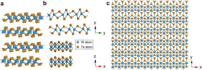
Transition metal dichalcogenides (TMDs) have attracted a lot of attention because of their emerging and remarkable electrical, optical and mechanical properties1,2. In contrast to the widely studied TMDs like MoS2, WS2, MoSe2, WSe2 and MoTe23,4,5, which are in-plane isotropous, WTe2 crystallizes in a distorted structure with an octahedral coordination around the metal, referred to as Td-polytype6. The recent discovery of non-saturating giant positive magnetoresistance and excellent thermoelectric behaviors in WTe2 arouses great interest in this material7,8,9. In addition, WTe2 is predicted to be a novel type of topological semimetal for further quantum transport studies10. The Td-WTe2 is constituted with triple-layer covalently bonded Te-W-Te atomic planes stacking along the c-axis through van der Waals interactions, as shown in Fig. 1a,b. The Td-WTe2 is strongly distorted from the ideal hexagonal net, because the off-centering W atoms form the slightly buckled W-W zigzag chains along the a-axis of the orthorhombic unit cell, as shown in Fig. 1c. The reduced crystal symmetry of WTe2 leads to the strong in-plane anisotropy.
Figure 1.
Crystalline structure of Td-WTe2, with (a) perspective view, (b) front view and side views, (c) top view.
Raman spectroscopy of both few-layer and bulk WTe2 was reported recently, which was crucial first step for WTe2 crystal structure characterization6,11,12,13,14. However, in order to further study the particular property of WTe2 and exploit related novel electronic and optoelectronic devices, more detailed study about few-layer and bulk WTe2 Raman spectra is still needed. In this work, we investigate the detailed Raman responses of both few-layer and bulk WTe2 flakes using the high-resolution angle-dependent and polarized Raman spectroscopy (ADPRS). The detected Raman modes are much more compared with the previous literatures6,11,12,13. By combining the symmetry analysis of the ADPRS results and the first principle calculation, we can accurately identify the symmetries of the detected modes and obtain the relation between their symmetries and lattice vibrations. We also identify the crystalline orientation of the WTe2 flakes based on the “in-plane anisotropy”, which is a precise and non-destructive all-optical method. Our work provides a deep understanding of the interaction between WTe2 and light, which will benefit in future studies about the anisotropic optical, electrical, and mechanical properties of WTe2 and other in-plane anisotropic materials15,16,17,18,19,20,21,22,23,24,25,26,27,28,29,30,31,32,33,34,35.
Results and Discussion
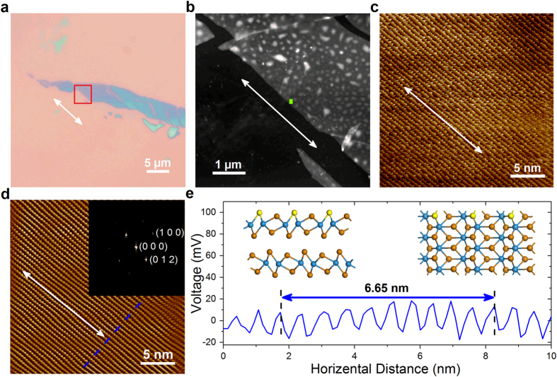
The Td-WTe2 bulk crystal used in this work was grown by the chemical vapor transport (CVT) method (more details in Method). The mono- and few-layer WTe2 were mechanically exfoliated on 300 nm SiO2/Si and quartz substrates (Supplementary Fig. S1) from the crystal. Figure 2a shows the optical microscope image of an as-exfoliated few-layer WTe2. Usually a well-defined edge (indicated by the white double-headed arrow) is naturally formed after exfoliation, due to the small cleave energy along the a-axis (i.e., the direction along the W-W chains). This is further confirmed by the quantitative atomic resolution force image probed by high-resolution atomic force microscopy (HR-AFM)36. Here, we define the a-axis as x-axis, the in plane direction perpendicular to it as y-axis, and the direction perpendicular to the 2D plane (c-axis) as z-axis. Figure 2b is an AFM image of the few-layer WTe2 (the red box area) in Fig. 2a. The corresponding HR-AFM image (the green box area) is shown in Fig. 2c. The smoothed HR-AFM image after the fast Fourier transform (FFT) is depicted in Fig. 2d. We can observe clearly one dimensional atomic chains parallel to the well-defined edge shown in Fig. 2a. The inset in Fig. 2d is the FFT image, where the distorted hexagon shape origins from the two different tungsten-tellurium bond lengths (2.7 Å and 2.8 Å). The height variation induced by the protruding tellurium atoms (highlighted in yellow in the inset) perpendicular to the one dimensional chains is shown in Fig. 2e. The average peak distance is about 6.65 Å, close to the lattice constant b.
Figure 2.
(a) Optical microscope image of the measured exfoliated WTe2 flake on SiO2/Si substrate. The white double-headed arrow indicates the well-defined edge, which is naturally formed after exfoliation. (b) AFM image of the red box area of the WTe2 depicted in (a). (c) HR-AFM image of the green box area of the WTe2 depicted in (b). (d) The smoothed HR-AFM image after FFT. The FFT image is shown in the inset. (e) The height variation profile perpendicular to the one dimensional chain along the dashed line in (d). The direction of well-defined edge in (a,b) and the direction along one dimensional chain in (c,d) are represented by white double arrows.
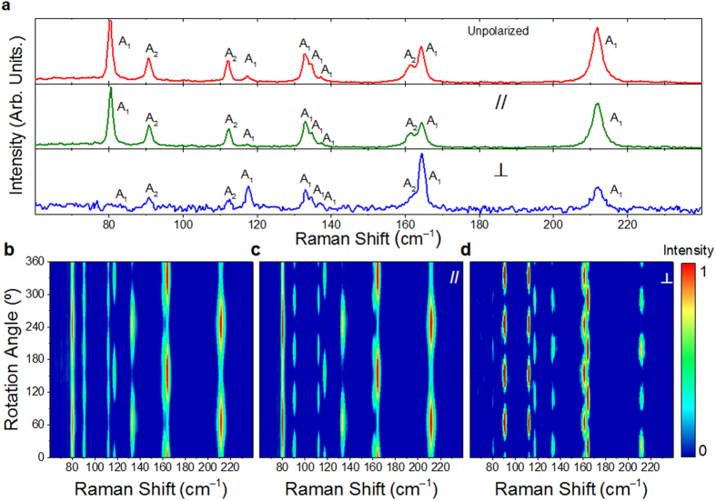
In the ADPRS measurement, a WTe2 flake on SiO2/Si substrate was initially placed with an arbitrary angle θ0 between the x-axis and horizontal direction. Herein, θ0 can be used to denote the crystalline orientation. We define θ0 to be positive (negative) value, when the x-axis is clockwise (anti-clockwise) compared to the horizontal direction (more details in Method and Supplementary Fig. S2). Figure 3a shows the Raman spectra of WTe2 in the un-, parallel- and cross-polarized configurations measured at an angle with the maximum number of Raman active modes. Altogether, ten Raman modes can be resolved. All of them can be well fitted by Lorentzian lineshape. Figure 3b–d show the angular dependences of the normalized Raman intensity spectra in the un-, parallel- and cross-polarized configurations, respectively. The sample rotation angle is in a range of 0–360°. The highest peak in each spectrum is used for normalization. We can see that, in the parallel-polarized configuration, the modes at ~80, 133, 135, 137 and 212 cm−1 yield 2-lobed shape with two maximum intensity angles at about 65° and 245°; the modes at ~117 and 164 cm−1 yield 2-lobed shape with two maximum intensity angles at about 155°and 335°; and the modes at ~91, 112 and 161 cm−1 yield 4-lobed shape with four maximum intensity angles at about 20°, 110°, 200° and 290°. In the cross-polarized configuration, all modes yield 4-lobed shape. The four maximum intensity angles for the modes at ~91, 112 and 161 cm−1 are θ = 65°, 155°, 245° and 335°, and those for the rest ones are 20°, 110°, 200° and 290°. In addition, we can see that the intensities of the three neighbored modes at 133, 135 and 137 cm−1 have similar angular dependent relations; while those of the two neighbored modes at 161 and 164 cm−1 have different angular dependent relations. The related angular dependent evolutions of these detected modes in the rotation angle range of 0–90° under the three polarized configurations are shown in Supplementary Figs S4–7, respectively. The ADPRS results for WTe2 with four representative different thicknesses (~3 nm, 10 nm, 25 nm and 40 nm) are shown in Supplementary Fig. S3. The results show that the anisotropic Raman spectra of WTe2 flakes have no clear thickness (≥3 nm) dependence.
Figure 3.
(a) Normalized Raman spectra measured at an angle where all modes appear in un-, parallel- and cross-polarized configurations. Angular dependence of the normalized Raman intensity spectra for the WTe2 flake measured in (b) un-polarized, (c) parallel-polarized and (d) cross-polarized configurations.
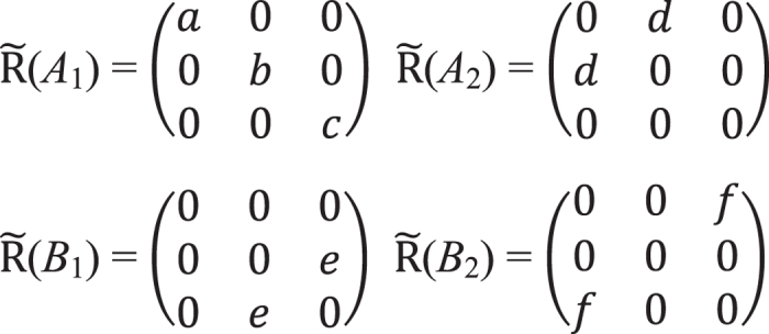
We can quantitatively analyze these observed anisotropic phenomena, based on the group theory, Raman tensors and density functional theory (DFT) calculations. According to symmetry analysis, the bulk Td-WTe2 belongs to the space group Pmn21 and point group  11,37. The unit cell of bulk Td-WTe2 contains two tungsten atoms and four tellurium atoms. There are 33 normal optical phonon modes at the Brillion zone center Г point, with irreducible representation as Гbulk = 11A1 + 6A2 + 5B1 + 11B2, where all the vibration modes are Raman active. The 11A1, 5B1 and 11B2 modes are also infrared active. There exists a correlation between the Raman tensors of bulk and few-layer WTe2 (more details in Supplementary Information). For simplicity, we use the Raman tensors of bulk WTe2 (Fig. 4) to do the analysis11,12.
Figure 4. Raman tensor forms for all Raman active modes in bulk WTe2.
According to the classical Placzek approximation, the Raman intensity of a phonon mode can be written as38:
 |
where ei and es are the electric polarization unitary vectors of the incident and scattered lights, respectively, and  is the Raman tensor. The Raman tensors for all Raman active modes in bulk WTe2 are given in Fig. 4. Based on the Cartesian coordinates denoted above, the ei and es are fixed in xy plane. For a sample with rotation angle of θ (clockwise rotation, as shown in Fig. S2), ei = (cos(θ + θ0) sin(θ + θ0) 0) for the incident light, and es = (cos(θ + θ0) sin(θ + θ0) 0) and (−sin(θ + θ0) cos(θ + θ0) 0) for the scattered light in the parallel- and cross-polarized configurations, respectively. A phonon mode can only be detected when
  has non-zero value. Therefore, in the backscattering geometry, only A1 and A2 Raman modes can be observed. Using the above defined unitary vectors ei and es, as well as the Raman tensors of A1 and A2 modes, we can obtain the angular dependent intensity expressions for the A1 and A2 modes to be:
 |
 |
 |
 |
As the initial angle θ0 is fixed, the intensity of A1 or A2 mode is a function of the corresponding elements of Raman tensor (a and b) and the rotation angle θ. In the parallel-polarized configuration, the angular dependence for the intensity of A1 mode has two cases, both of which have a variation period of 180°. For A1 mode with a > b, the maximum intensity appears at θ = 180° − θ0 and 360° − θ0, corresponding to the incident light polarization parallel to the W-W chains. On the contrary, the minimum intensity appears at θ = 90° − θ0 and 270° − θ0, corresponding to the incident light polarization perpendicular to the W-W chains. For the A1 mode with a < b, the maximum intensity angles are θ = 90° − θ0 and 270° − θ0, and the minimum intensity angles are θ = 180° − θ0 and 360° − θ0, corresponding to the incident light polarization perpendicular and parallel to the W-W chains, respectively. In the parallel-polarized configuration, the angular dependence for the intensity of A2 mode has a variation period of 90° with the maximum intensity at θ = 45° − θ0, 135° − θ0, 225° − θ0 and 315° − θ0, and the minimum intensity at θ = 90° − θ0, 180° − θ0, 270° − θ0 and 360° − θ0. In the cross-polarized configuration, both of A1 and A2 modes have a variation period of 90°. The intensity of A1 mode (A2 mode) reaches its maximum (minimum) at θ = 45° − θ0°, 135° − θ0, 225° − θ0 and 315° − θ0, and reaches its minimum (maximum) at θ = 90° − θ0, 180° − θ0, 270° − θ0 and 360° − θ0. In addition, the normalized Raman intensities of the ten detected modes (except for A2 modes) in un-polarized configuration exhibit similar angular dependences to those in parallel-polarized configuration, as shown in Supplementary Fig. S8. It is worth noting that, as sample rotates, the full width at half maximum (FWHM) of each detected mode keeps almost constant, as shown in Supplementary Fig. S9.
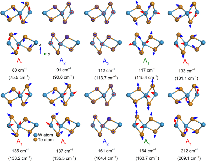
According to the above analysis, we can use the ADPRS to identify the symmetries of the detected modes. The intensity variation periods for A1 modes are 180° and 90° in parallel- and cross-polarized configurations, respectively, while those for A2 phonon modes are 90° in both configurations. Therefore, seven phonon modes located at ~80, 117, 133, 135, 137, 164 and 212 cm−1 belong to A1 modes, and three modes located at ~91, 112 and 161 cm−1 belong to A2 modes. In addition, we find that when the incident polarization is parallel to the well-defined edge (i.e. parallel to the W-W chains) of the sample, the Raman modes at 117 and 164 cm−1 reach their maximum intensities. Therefore, we assign them to A1 modes with a > b. The rest A1 modes are with a < b. The lattice vibrations of all phonon modes are calculated by the density functional theory (DFT, more details in Method, Supplementary Fig. S11 and Table S1), and atomic displacements of detected ones are shown in Fig. 5. Because monolayer WTe2 (with space group P21/m and point group  ) has different crystal symmetry with the bulk one, the 2-lobed modes in monolayer WTe2 can be labelled as Ag, and the 4-lobed ones can be labelled as Bg. Notably, there is no odd and even layer number dependence of crystal symmetry for WTe2. Therefore, for N-layer WTe2 (N ≥ 2, with space group Pm and point group
  ), the 2-lobed and 4-lobed modes can be labelled as A′ and A″, respectively.
Figure 5. The calculated atomic displacements for the lattice vibrations of the ten detected modes in WTe2, together with their corresponding irreducible representations.
The theoretical frequency is given below its experimental counterpart in each plot. The motions of W (Te) atoms are presented by red (blue) arrows.
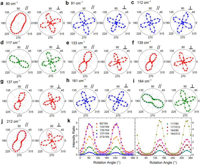
Notably, according to above results, we can use the maximum intensity of the mode at ~164 cm−1 in un- and parallel-polarized configurations to identify the crystallographic orientation (i.e. the direction of W-W chains) rapidly and nondestructively. This is important in case that the well-defined edge of a few-layer WTe2 cannot be easily identified by the optical microscopy. In our case, it is represented by θ0 ~ 25°. The angular dependence of the normalized Raman intensities for the ten detected modes in the parallel- and cross-polarized configurations are shown in the polar plots in Fig. 6a–j. Notably, since the opposite angular dependent relations for A1 modes with a < b and a > b, their intensity ratio shows a clearer 2-lobed characteristic with sample rotating, as shown in Fig. 6k. By curving fitting Fig. 6k, we can obtain a more accurate θ0 to be 27.5°. The angular dependences of the Raman intensity ratios between other A1 and A2 modes, which are also helpful for identifying the crystallographic orientation, are shown in Supplementary Fig. S10.
Figure 6.
Angular dependence of the Raman intensities for the detected ten modes (a–j) in the parallel and cross polarization configurations. The experimental data are the scattered dots, and the curve fitting results are the solid lines. The intensity for each mode is normalized to its maximum value. Three types of modes, which have different angular dependent relations are colored in red, green and blue, respectively. (k) Angular dependence of the Raman intensity ratio for A1 modes with a < b and a > b in the parallel-polarized configuration. The curving fitting results are the solid lines.
It is worth noting that, the polar plots of A1 modes with higher frequencies (164 and 212 cm−1) in Fig. 6i,j cannot be well fitted by equation (2) (the blue and purple lines are the corresponding fitting results). In order to explain this, we consider the light absorption effect on the Raman tensor elements38,39. In an absorptive material, the elements of the Raman tensor should be complex numbers, with real and imaginary parts. In this case, the tensor elements of A1 and A2 can be written as
 |
where ϕa, ϕb and ϕd are the corresponding phases. Substituting in equation (1) with the unitary vectors ei and es and the above Raman tensor elements, we can modify the angular dependent intensity expressions of the A1 and A2 modes as:
 |
 |
 |
 |
where ϕba = ϕb − ϕa is the phase difference between the Raman tensor elements b and a. The expressions for A2 modes (equations 9 and 10) are identical to their counterparts (equations 4 and 5) obtained considering only real part of the Raman tensor elements. However, the expressions for A1 modes are different. We can see that the absorption effect on the ADPRS reflects in phase difference. The angular dependent intensities of A1 modes at 164 and 212 cm−1 can be well fitted by equations (7) and (8), as shown in Fig. 6i,j.
To further characterize the vibration direction of atoms for these detected modes. We choose defined x, y and z axes as the reference directions. Compared with the typical atomic displacements in 2H-type TMDs, such as MoS2, WS2, MoSe2 and WSe2 etc., the atomic displacements in WTe2 is relative complicated and disordered due to the lower symmetry. The related Raman tensor element ratios (b/a), phase differences, and shrinkage degrees for the ten detected modes are summarized in Table 1. Here, we define the shrinkage degree as the ratio of the maximum intensity and its orthogonal direction intensity in a polar plot. Considering the absorption effect, we can obtain the shrinkage degrees for A1 modes to be: 
 and
and 
 , and those for A2 modes are closer to one. We find that the shrinkage degree reflects the vibrational tendency and complexity of detected modes. Specifically, the modes with smaller shrinkage degrees have the tendency to vibrate along the axes, and the ones with larger shrinkage degrees have the tendency to vibrate away from the axes. For three A2 modes, whose shrinkage degrees are close to one (minimum value), both W and Te atoms vibrate along the W-W chains (x-axis). In the case of A1 modes with relative small shrinkage degrees, for the A1 mode at ~80 cm−1, all the W atoms have the tendency to vibrate along the z axis, and half of the Te atoms have the tendency to vibrate along the y axis. For the A1 mode at ~164 cm−1, all the W (Te) atoms have the tendency to vibrate along the y (z) axis. For the A1 mode at ~212 cm−1, all the W (Te) atoms have the tendency to vibrate along the z (y) axis. For the rest four A1 modes with larger shrinkage degrees, their vibrations are more complicated. This finding may be applied for studying the complicated atomic vibrations in other anisotropic materials.
Table 1. The irreducible representations, calculated frequencies Raman tensor elements ratio b/a, cos ϕba and shrinkage degrees for all the detected phonon modes.
| Experimental frequency (cm−1) | 80 | 91 | 112 | 117 | 133 | 135 | 137 | 161 | 164 | 212 |
|---|---|---|---|---|---|---|---|---|---|---|
| Irreducible representation | A1 | A2 | A2 | A1 | A1 | A1 | A1 | A2 | A1 | A1 |
| Calculated Frequency (cm−1) | 75.5 | 90.8 | 113.7 | 115.4 | 131.1 | 133.2 | 135.5 | 164.4 | 163.7 | 209.1 |
| Raman tensor elements ratio b/a | ~0.71 | – | – | ~16.7 | ~0.30 | ~0.22 | ~0.10 | – | ~2.45 | ~0.49 |
| cos ϕba | ~1 | – | – | ~1 | ~1 | ~1 | ~1 | – | ~0.50 | ~0.68 |
| Shrinkage degree | ~1.98 | ~1.00 | ~1.00 | ~279 | ~11.1 | ~20.7 | ~100 | ~1.00 | ~3.72 | ~3.84 |
Conclusion
In this work, we study the ADPRS of WTe2. Ten Raman modes are clearly resolved. Their intensities show periodic variation with sample rotating. We identify the symmetries of these detected modes by quantitatively analyzing the ADPRS results using the symmetry selection rules based on the Raman tensors, and do the curve fitting to the angular dependent intensities of them using the complex Raman tensor elements induced by absorption effect. We also provide a rapid and nondestructive method to identify the crystallographic orientation of WTe2. We find that the defined shrinkage degree based on ADPRS also reflects the vibrational tendency and complexity of the detected modes, which is confirmed by their atomic vibrations calculated by density functional theory. Our work provides a deep understanding of the interaction between WTe2 and light, which will benefit in future studies about the anisotropic optical, electrical, and mechanical properties of WTe2 as well as other in-plane anisotropic materials.
Methods
Growth of bulk WTe2
WTe2 single crystals were grown by the CVT method8. Stoichiometric W and Te powders were ground together and loaded into a quartz tube with a small amount of TeBr4 (transport agent). All weighing and mixing were carried out in a glove box. The tube was sealed under vacuum and placed in a two-zone furnace. The hot and cold zones were maintained at 800 °C and 700 °C, respectively, for 10 days. The crystal product appeared in cold zone.
Measurements
The quantitative atomic resolution force image of WTe2 was measured by HR-AFM (Bruker Dimension Icon-PT). The angle- and polarization- resolved Raman spectra of exfoliated MoTe2 on 300 nm SiO2/Si substrate were measured by a commercial micro-Raman system (Horiba Jobin Yvon HR800) under the backscattering geometry. In order to obtain high-resolution spectra, we used a 100× object lens, and the grating with 1800 or 2400 grooves/mm. The exposure time is 100 seconds. The excitation wavelength was 633 nm, and the light power was below 400 μW. The incident light was polarized along the horizontal direction. The parallel- and cross-polarized configurations were constructed by placing an analyzer before the spectrometer.
Density Functional Calculations
The calculations of phonon spectra were performed within local-density appreciation (LDA) using projector-augmented wave potentials. A 3 × 2 × 1 supercell was created and the interatomic forces were computed using the Vienna ab initio simulation package code with the small displacements method40. From these, force constant matrices and phonon frequencies were extracted using the PHONOPY Code41. The kinetic energy cutoff of the plane-wave basis was set to be 350 eV and 3 × 2 × 2 Monkhorst Pack grid was used in the phonon calculation.
Additional Information
How to cite this article: Song, Q. et al. The In-Plane Anisotropy of WTe2 Investigated by Angle-Dependent and Polarized Raman Spectroscopy. Sci. Rep. 6, 29254; doi: 10.1038/srep29254 (2016).
Supplementary Material
Acknowledgments
We acknowledge support from the National Key Projects for Basic Research Program of China (2013CB921901, 2012CB932703, 2013CB922103, and 2011CB922103), the National Natural Science Foundation of China (Grants nos 61521004, 61125402, 51172004, 11474007, 11225421, 11434010, 11474277, 91421109, 11134005, 61176088, 11522432, 11525417, 11274003, 61176079, 21373156 and 11404253).
Footnotes
Author Contributions Q.S. and L.D. designed the experiments and did the analysis. X.P. and F.S. grew the bulk WTe2 sample. H.W., P.L. and X.W. did the density functional calculations. Q.S., K.Z., Q.T., X.X., M.L. and L.D. contributed to the Raman measurements. Q.S., Yi Wan and Yilun Wang contributed to the measurements of atomic force microscope. Q.S. and L.D. wrote the paper and all authors helped with the revisions. We also thank Prof. Pingheng Tan from the Institute of Semiconductors, Chinese Academy of Sciences for helpful discussion.
References
- Zhang Y., Tan Y. W., Stormer H. L. & Kim P. Experimental observation of the quantum Hall effect and Berry’s phase in graphene. Nature 438, 201–204, 10.1038/nature04235 (2005). [DOI] [PubMed] [Google Scholar]
- Mak K. F., He K., Shan J. & Heinz T. F. Control of valley polarization in monolayer MoS2 by optical helicity. Nature nanotechnology 7, 494–498, 10.1038/nnano.2012.96 (2012). [DOI] [PubMed] [Google Scholar]
- Zhang X. et al. Phonon and Raman scattering of two-dimensional transition metal dichalcogenides from monolayer, multilayer to bulk material. Chemical Society Reviews 44, 2757–2785, 10.1039/c4cs00282b (2015). [DOI] [PubMed] [Google Scholar]
- Froehlicher G. et al. Unified Description of the Optical Phonon Modes in N-Layer MoTe2. Nano letters 15, 6481–6489, 10.1021/acs.nanolett.5b02683 (2015). [DOI] [PubMed] [Google Scholar]
- Song Q. J. et al. Physical origin of Davydov splitting and resonant Raman spectroscopy of Davydov components in multilayer MoTe2. Physical Review B 93, 10.1103/PhysRevB.93.115409 (2016). [DOI] [Google Scholar]
- Lee C. H. et al. Tungsten Ditelluride: a layered semimetal. Scientific reports 5, 10013, 10.1038/srep10013 (2015). [DOI] [PMC free article] [PubMed] [Google Scholar]
- Ali M. N. et al. Large, non-saturating magnetoresistance in WTe2. Nature 514, 205–208, 10.1038/nature13763 (2014). [DOI] [PubMed] [Google Scholar]
- Pan X. C. et al. Pressure-driven dome-shaped superconductivity and electronic structural evolution in tungsten ditelluride. Nature communications 6, 7805, 10.1038/ncomms8805 (2015). [DOI] [PMC free article] [PubMed] [Google Scholar]
- Pletikosic I., Ali M. N., Fedorov A. V., Cava R. J. & Valla T. Electronic structure basis for the extraordinary magnetoresistance in WTe2. Physical Review Letters 113, 216601, 10.1103/PhysRevLett.113.216601 (2014). [DOI] [PubMed] [Google Scholar]
- Soluyanov A. A. et al. Type-II Weyl semimetals. Nature 527, 495–498, 10.1038/nature15768 (2015). [DOI] [PubMed] [Google Scholar]
- Kong W. D. et al. Raman scattering investigation of large positive magnetoresistance material WTe2. Applied Physics Letters 106, 081906, 10.1063/1.4913680 (2015). [DOI] [Google Scholar]
- Jiang Y. C., Gao J. & Wang L. Raman fingerprint for semi-metal WTe2 evolving from bulk to monolayer. Scientific reports 6, 19624, 10.1038/srep19624 (2016). [DOI] [PMC free article] [PubMed] [Google Scholar]
- Kim Y. et al. Anomalous Raman scattering and lattice dynamics in mono- and few-layer WTe2. Nanoscale 8, 2309–2316, 10.1039/c5nr06098b (2016). [DOI] [PubMed] [Google Scholar]
- Lee J. et al. Single- and few-layer WTe2 and their suspended nanostructures: Raman signatures and nanomechanical resonances. Nanoscale 8, 7854–7860, 10.1039/c6nr00492j (2016). [DOI] [PubMed] [Google Scholar]
- Ribeiro H. B. et al. Unusual Angular Dependence of the Raman Response in Black Phosphorus. ACS Nano 9, 4270–4276, 10.1021/acsnano.5b00698 (2015). [DOI] [PubMed] [Google Scholar]
- Wu J., Mao N., Xie L., Xu H. & Zhang J. Identifying the crystalline orientation of black phosphorus using angle-resolved polarized Raman spectroscopy. Angewandte Chemie 54, 2366–2369, 10.1002/anie.201410108 (2015). [DOI] [PubMed] [Google Scholar]
- Chenet D. A. et al. In-Plane Anisotropy in Mono- and Few-Layer ReS2 Probed by Raman Spectroscopy and Scanning Transmission Electron Microscopy. Nano letters 15, 5667–5672, 10.1021/acs.nanolett.5b00910 (2015). [DOI] [PubMed] [Google Scholar]
- Homes C. C., Ali M. N. & Cava R. J. Optical properties of the perfectly compensated semimetal WTe2. Physical Review B 92, 161109, 10.1103/PhysRevB.92.161109 (2015). [DOI] [Google Scholar]
- Luo Z. et al. Anisotropic in-plane thermal conductivity observed in few-layer black phosphorus. Nature communications 6, 8572, 10.1038/ncomms9572 (2015). [DOI] [PMC free article] [PubMed] [Google Scholar]
- Tao J. et al. Mechanical and Electrical Anisotropy of Few-Layer Black Phosphorus. ACS Nano 9, 11362–11370, 10.1021/acsnano.5b05151 (2015). [DOI] [PubMed] [Google Scholar]
- Fei R. & Yang L. Strain-engineering the anisotropic electrical conductance of few-layer black phosphorus. Nano letters 14, 2884–2889, 10.1021/nl500935z (2014). [DOI] [PubMed] [Google Scholar]
- Liu E. et al. Integrated digital inverters based on two-dimensional anisotropic ReS2 field-effect transistors. Nature communications 6, 6991, 10.1038/ncomms7991 (2015). [DOI] [PMC free article] [PubMed] [Google Scholar]
- Xia F., Wang H. & Jia Y. Rediscovering black phosphorus as an anisotropic layered material for optoelectronics and electronics. Nature communications 5, 4458, 10.1038/ncomms5458 (2014). [DOI] [PubMed] [Google Scholar]
- Lin Y. C. et al. Single-Layer ReS2: Two-Dimensional Semiconductor with Tunable In-Plane Anisotropy. ACS Nano 9, 11249–11257, 10.1021/acsnano.5b04851 (2015). [DOI] [PubMed] [Google Scholar]
- Aslan O. B. et al. Linearly Polarized Excitons in Single- and Few-Layer ReS2 Crystals. ACS Photonics 3, 96–101, 10.1021/acsphotonics.5b00486 (2015). [DOI] [Google Scholar]
- Wolverson D. et al. Raman Spectra of Monolayer, Few-Layer, and Bulk ReSe2: An Anisotropic Layered Semiconductor. ACS Nano 8, 11154–11164, 10.1021/nn5053926 (2014). [DOI] [PubMed] [Google Scholar]
- Zhao H. et al. Interlayer interactions in anisotropic atomically thin rhenium diselenide. Nano Research 8, 3651–3661, 10.1007/s12274-015-0865-0 (2015). [DOI] [Google Scholar]
- Zhang E. et al. ReS2-Based Field-Effect Transistors and Photodetectors. Advanced Functional Materials 25, 4076–4082, 10.1002/adfm.201500969 (2015). [DOI] [Google Scholar]
- Zhong H.-X., Gao S., Shi J.-J. & Yang L. Quasiparticle band gaps, excitonic effects, and anisotropic optical properties of the monolayer distorted 1T diamond-chain structures ReS2 and ReSe2. Physical Review B 92, 10.1103/PhysRevB.92.115438 (2015). [DOI] [Google Scholar]
- Nagler P., Plechinger G., Schüller C. & Korn T. Observation of anisotropic interlayer Raman modes in few-layer ReS2. physica status solidi (RRL) - Rapid Research Letters 10, 185–189, 10.1002/pssr.201510412 (2015). [DOI] [Google Scholar]
- He R. et al. Coupling and Stacking Order of ReS2 Atomic Layers Revealed by Ultralow-Frequency Raman Spectroscopy. Nano letters, 16, 1404–1409, 10.1021/acs.nanolett5b04925 (2016). [DOI] [PubMed] [Google Scholar]
- Liu E. et al. High responsivity phototransistors based on few-layer ReS2 for weak signal detection. Nature communication 6, 6991, 10.1038/ncomms7991 (2015). [DOI] [Google Scholar]
- Qiao X. F. et al. Polytypism and Unexpected Strong Interlayer Coupling of two-Dimensional Layered ReS2. Nanoscale, 8, 8324–8332, 10.1039/C6NR01569G (2016). [DOI] [PubMed] [Google Scholar]
- Ling X. et al. Anisotropic Electron-Photon and Electron-Phonon Interactions in Black Phosphorus. Nano letters 16, 2260–2267, 10.1021/acs.nanolett.5b04540 (2016). [DOI] [PubMed] [Google Scholar]
- Lorchat E., Froehlicher G. & Berciaud S. Splitting of Interlayer Shear Modes and Photon Energy Dependent Anisotropic Raman Response in N-Layer ReSe2 and ReS2. ACS Nano 10, 2752–2760, 10.1021/acsnano.5b07844 (2016). [DOI] [PubMed] [Google Scholar]
- Boneschanscher M. P. et al. Quantitative Atomic Resolution Force Imaging on Epitaxial Graphene with Reactive and Nonreactive AFM Probes. ACS Nano 6, 10216–10221, 10.1021/nn3040155 (2012). [DOI] [PubMed] [Google Scholar]
- Mar A., Jobic S. & Ibers J. A. Metal-Metal vs Tellurium-Tellurium Bonding in WTe2 and Its Ternary Variants TaIrTe4 and NbIrTe4. J. Am. Chem. SOC 114, 8963–8971 (1992). [Google Scholar]
- Loudon R. The Raman effect in crystals. Advances in Physics 13, 423–482, 10.1080/00018736400101051 (1964). [DOI] [Google Scholar]
- Cardona M. In Light Scattering in Solids II. Vol. 50, Ch. 2, 19–278 (Springer, 1982). [Google Scholar]
- Kresse G., Furthmüller J. & Hafner. Ab initio Force Constant Approach to Phonon Dispersion Relations of Diamond and Graphite. Europhys. Lett. 32, 729–734 (1995). [Google Scholar]
- Togo A., Oba F. & Tanaka I. First-principles calculations of the ferroelastic transition between rutile-type and CaCl2-type SiO2 at high pressures. Physical Review B 78, 134106, 10.1103/PhysRevB.78.134106 (2008). [DOI] [Google Scholar]
Associated Data
This section collects any data citations, data availability statements, or supplementary materials included in this article.


