Abstract
Inductive powering of implantable medical devices involves numerous factors acting on the system efficiency and safety in adversarial ways. This paper lightens up their role and identifies a procedure enabling the system design. The latter enables the problem to be decoupled into four principal steps: the frequency choice, the magnetic link optimization, the secondary circuit and then finally the primary circuit designs. The methodology has been tested for the powering system of a device requirering a power of 300mW and implanted at a distance of 15 to 30mm from the outside power source. It allowed the identification of the most critical parameters. A satisfying efficiency of 34% was reached at 21mm and tend to validate the proposed design procedure.
Key Words: implanted neurostimulators, inductive powering, design methodology, efficiency optimisation
The use of inductive powering systems for implantable stimulators has risen unceasingly over the last years since this non-invasive technology offers an unlimited controllable power source, coping with problems of non-rechargeable batteries or percutaneous electrodes leads. Batteries present a limited lifetime requiring regular surgical operations for replacement. Moreover, the limitation on the size of the implanted systems strongly restricts the energy budget of the battery.1 Inductive powering is based on the magnetic coupling of two coils: one (coil 1) outside the body, transmitting the energy, and another (coil 2) implanted within the body, receiving the energy. This energy is delivered to a rechargeable battery or can be used directly by the implant to perform the stimulation. The energy provided to the primary circuit by a dc supply source is converted into an alternative signal by a power amplifier (PA). This signal flows through the primary coil and generates an oscillating magnetic field sensed by the secondary coil inside the body. Magnetic energy is then transformed to electrical energy via a resonant secondary circuit. Finally, it is turned into a dc signal by a power rectifier.
Despite its widespread use, inductive powering technology still presents numerous challenges when it comes to applying it to implantable medical devices. The complexity of the interactions between the different factors on which the power transfer system (PTS) relies implies an in-depth study leading to the identification of a reliable and efficient design procedure The proposed paper consolidates current literature to produce a coherent methodology that is validated on a case study through simulations and measurements.
Materials and Methods
The global design methodology chart flow is presented in Fig. 1. The system can be decoupled according to its physical and electrical parts. Two main aspects are thus to be considered for the design methodology: the magnetic link design and the electronic design. The magnetic link design is based on the optimization of the magnetic coupling between the transmitter and the receiver, and aims to minimize the power loss between them. It only depends on the material properties and the coil geometries and placement. It is therefore the first step of the design procedure. The electronic design can in itself be split into two steps: the design of the secondary circuit and then the determination of the primary circuit components. This division into sub-systems is convenient to tune each oscillating circuit individually. It reduces the risk of having to change the secondary coil or circuit after a modification of the primary circuit. Subsequently, it limits the number of iterations of the design procedure. In this paper, we present an example of an application for this methodology with given specifications: constant 60mA current through a load at 5V nominal voltage; a nominal transfer distance z of 15 mm between transmitter and receiver coils, while the outer diameter dout2 of the implanted coil should not exceed 26 mm.
Fig 1.
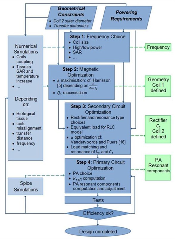
Design methodology chart flow presenting the different steps to follow from the initial requirements and constraints to the obtainment of an efficient power transfer system, and the possible simulations to perform in parallel in order to improve the analytical and experimental process.
Step 1: Frequency Choice
The choice of the operating frequency is highly critical. The magnetic link efficiency increases when the coupling coefficient k and the quality factors of the coils Q1 and Q2 increase (see section B.). Regarding the coupling coefficient, it can be enhanced by using larger coils that imply using a lower frequency. Besides, a decrease in frequency leads to the reduction of the quality factors of the coils. On the other hand, the choice of a higher frequency leads to a higher energy absorption by the patient’s tissues. Moreover, higher frequencies will affect the power amplifier and rectifier efficiencies and enlarge the undesired equivalent series resistance ESR of the coils because of the skin and proximity effects.2 Besides, designers should also keep in mind the allowable frequency allocation for medical devices 3.
Considering those facts, inductive powering systems for medical implants generally operate in the range of hundreds of kilohertz to several tens of Megahertz.4-12 To clarify the problem, the choice of the working frequency has been defined at the beginning of the procedure. Considering the small size of the coils generally designed for industrial purposes, 6.78 MHz, the lowest FCC-approved ISM frequency13 was chosen
Step 2: Magnetic Link Design
The magnetic link efficiency between the transmitter and receiver coils is directly proportional to the design factor X = K2Q1Q2 1,4, where k is the coupling coefficient, a dimensionless quantity equal to the fraction of the magnetic flux generated by the primary coil that flows through the secondary coil, and where Qi are the quality factors of the respective coils characterizing the ratio of the stored energy to the energy dissipated in the coils. Eq. 1 is an approximation of the Q-factors valid for inductive powering coils4,5:
| (1) |
where ω is the angular resonant frequency, Li and Ri are respectively the self-inductances and the ESR of the coils i.
Optimizing the magnetic link is performed by maximizing the coupling coefficient and the coils quality factors. However, there is a limit on Q1 since it could lead to a high and dangerous voltage at the extremities of the coil 1.4 The coupling coefficient does not depend on the circuit topology. Also, since the mutual inductance M is proportional to N1N2, and Li proportional to Ni2, k does not depend on the number of coil turns. The main focus of the magnetic design consists thus in maximizing k by fixing appropriate coil geometries as suggested by R. R. Harrisson.4 The latter uses the current sheet approximation to analytically compute the inductance of planar spiral coils.4,14,15 This type of coils is the most appropriate for subcutaneous applications as they offer the most comfort6 and as they present a remarkable mutual inductance.7,8 M can be estimated by calculating the mutual inductances between two pairs of circular single coils equivalent to the spiral coils.4,7 Harrisson’s methodology for maximum coupling leads to the coils outer and inner diameters douti, dini depending on the ratio of the transfer distance and the outer diameter of the receiver Z/dout2, which are the system main geometrical constraints. Once this geometry is fixed, coil 1 can be defined, enhancing Q1 by determining the appropriate number of turns and choosing wires of specific diameters. Proximity and skin effects should also be considered: Litz wires are recommended to reduce the coils ESR.5,16,17 Only the gross geometry of the coil 2 is defined at this stage: L2 and Q2 impact the secondary circuit efficiency and will be designed to match the load corresponding to the power requirements. The use of magnetic materials could improve the coupling between the coils, but this has not been considered in the present paper. Moreover, magnetic materials can have a dangerous impact when it comes to MRI compatibility.
Table 1 presents the results obtained at the end of the magnetic design for our example. Coil 1 is defined and has an inductance of 19μH.
Table 1.
Magnetic Design Outputs (where z is the transfer distance between the coils)
| Coil 1 | Coil 2 | |
|---|---|---|
| Outer diameter (mm) | 56.0 | 25.4 |
| Inner diameter (mm) | 11.2 | 16.3 |
| Turns number | 26 | Not defined |
| Coupling coefficient | 0.15 (at z=15mm) | |
Step 3: Secondary Circuit Design
The first part of the secondary circuit design consists in choosing a rectifier. Here, we suggest a reliable and simple full-bridge rectifier9 since the secondary voltage is expected large enough to provide the required output voltage despite the two diodes voltage drops. An equivalent load Rload representing the rectifier and the output load RDC is calculated according to Eq. 2.12 The circuit is then represented by a simple RLC model.
| (2) |
where Vout the output voltage of the PTS and Vdiode the diodes forward voltage. Secondly, the choice of the resonant capacitor C2 and the receiver coil configuration is made. Series-resonant drivers act as current sources while parallel-resonant drivers act as voltage sources. The decision depends on the value of the load and on the rectifier. A parallel circuit appeared the most suited for this system.1,11,12
Then, the number of turns N2 and the inductance L2 of the coil 2 is determined. In order to enhance the system efficiency, it is important to match the resonant components L2 and C2 to the load. It is done via the optimization of the efficiency with respect to the parameter α defined by G. Vandervoorde and R. Puers 11 as a dimensionless quantity corresponding to the ratio of Rload to the reactance of C2. Depending on the resonant circuit type, the efficiency formula varies and is developed in.1 The α obtained at maximum efficiency αopt (Eq. 4)11 allows the computation of C2 in function of the load (Eq. 5). L2 is finally deduced from equation of parallel RLC resonance (Eq. 6).
| (3) |
| (4) |
| (5) |
| (6) |
Since the calculation of coil 2 parameters depends on its quality factor Q2, the previous computations consist in several iterations, starting with a first estimation of Q2 (typically between 10 and 200).16 At each iteration, new values are calculated for C2, L2 and ESR2 until the value of Q2 is stable. Once L2 is determined, and since the geometrical dimensions have been defined during the magnetic design, N2 is given by to the current sheet approximation.14 The circuit on the right of Fig 3 is obtained at this stage. Coil 2 is now defined: it has3 turns (see Fig. 2) and an inductance of 0.48µH. The impedance of the secondary circuit will be seen by the primary circuit through the magnetic link: it is called the reflected impedance Rrefl which is real if the operating frequency is equal to the secondary resonant frequency. Depending on the coupling strength, Rrefl will influence more or less the transmitter circuit.18-20 This is the reason why the secondary circuit is designed before the primary.
Fig 3.
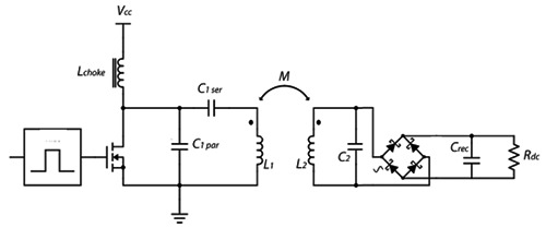
Power transfer system PTS obtained at the end of the design methodology for our example.
Fig 2.
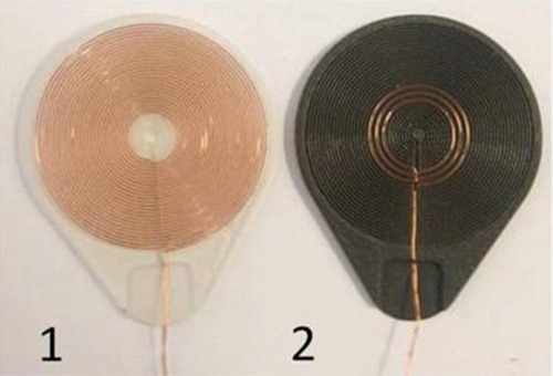
Designed Coils where the coil 1 and 2 are respectively the primary and the secondary coils
Step 4: Primary Circuit Design
Once the secondary circuit has been fixed, the primary circuit is conceived. First of all, the PA is chosen. It is then necessary to adapt the driving circuit components in function of the coil impedance, the frequency, the reflected impedance (if the coupling is important enough to have a significant influence on the PA operation) and the coils coupling. The class E PA is chosen because of its high efficiency especially for frequencies in the range of 3MHz to 1GHz.19 The PA efficiency is essentially due to the minimization of the power loss obtained by preventing the current to flow through the transistor when its drain-source voltage Vds is not zero, and vice-versa. It is necessary to adapt the components to the primary load i.e. to Rrefl (Eq. 7 for a parallel secondary circuit) ESR1, and the driver output impedance in order to approach the targeted signals.
| (7) |
Frederick H. Raab12,21 designed equations particularly appropriate for inductive powering systems allowing to get the tuning components estimation1. The effective components values differ from those ideally designed: it is possible to adjust them to obtain effectively a high efficiency operation by using Sokal’s method.19 Once this adjustment is done, the complete design optimizing the efficiencies of the magnetic link, the secondary and the primary circuits, is finished. The circuit (Fig. 3) can be tested for its output power and efficiency.
Results
The results of this section correspond to coils laterally and angularly aligned separated by an air gap of 10 to 30mm. Fig. 4 represents the total efficiency (i.e. the ratio of the output power at RDG to the input power from the supply), the efficiency before rectification (i.e. the ratio of the power received at the secondary coil to the input power from the supply) and the output power of the PTS. This result is obtained by varying the value of the C1ser capacitor (see Fig. 3) around the ideal class E operating point for a switch command frequency of 6.78MHz. The maximum total efficiency does not correspond to the ideal class E operating point (measure 6 on Fig. 1) where the drain voltage and its derivative are zero at transistor switch on. However, that point corresponds to the maximal efficiency before the signal rectification. At this operating point, the overall efficiency is 17.8% and the efficiency without the rectification is 49.3%. Since the high rectification losses reduce consequently the overall efficiency, Schottky diodes are used for the rectifier in the subsequent text (e.g. Fig. 5 & 6). Regarding the output power, it rises until its maximum of 325mW corresponding to a system efficiency of 24.4%. Fig. 4 helps to understand the implication of the different sources of power loss: the PA, the loose coupling, and the rectifier. Since the magnetic loss is related to the link gain depending only on the geometry, the principal factor influencing the efficiency before rectification is the PA. This explains that the best efficiency before rectification is found at the class E operating point. For subsequent measures (for which the switch command frequency is higher than the resonant frequency), the decrease of output power and efficiency is due to the PA losses. When the PA is switched at a frequency lower than the frequency needed to get the right class E operation, the output power and the overall efficiency rise despite the class E losses: for those operating frequencies, the input consumption increases which also increases the primary coil voltage. Since the gain is nearly constant, the secondary voltage increases too and enhances the rectifier efficiency.9 The decrease of the output power and of the efficiency only appears when these power gains cannot compensate the losses in the PA switch anymore. Fig. 5 shows that the maximal transfer efficiency and output power are obtained around a transfer distance of 16mm. For 8V supply, the efficiency reaches 38.1% and the output power equals 244mW. The improvement in efficiency compared to Fig. 4 (where the maximum efficiency was only 24.4%) is due to the use of Schotkky diodes. The transfer distances considered for the subcutaneous implant are generally ranging from 15 to 20 mm. At 20mm, the efficiency is still of 32.6% for an output power of 208mW. Fig. 6 shows that the PTS enables to deliver more than the targeted 300mW required by the initial power demand to the load for a supply voltage of 9V and a transfer distance of 21 mm. The corresponding efficiency is of 33.3%.
Fig 4.
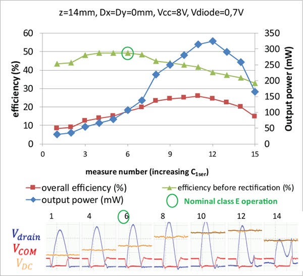
Efficiency before and after rectification, output power and screenshots of drain voltage Vdrain, gate voltage VCOM and voltage at the load VDC for different class E power amplifier operating points.
Fig 5.
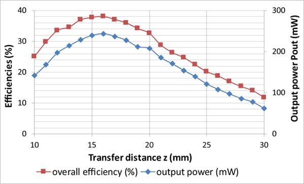
System efficiency and output power variation with the transfer distance z. Supply voltage Vcc=8V; Rectifiction diodes forward voltage Vdiode=0.35V.
Fig 6.
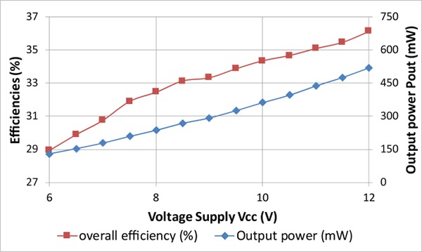
System efficiency and the output power variation with the supply voltage. Power transfer distance z=21mm; Rectification diodes forward voltage Vdiode=0.35V.
Discussion
Tests on efficiency and output power tend to validate the proposed design procedure: it leads to a system presenting a large efficiency (e.g. up to 34% at 21mm). For the secondary circuit, the rectification efficiency can become highly critical, in particular for low power applications with weak link gain. Therefore, high primary voltage is usually needed and class E PA are recommended. A trade-off can be found between the losses of the primary and the secondary circuits in order to maximize the efficiency and the expected output power over the required range of transfer distance.
This methodology presents some limitations: depending on the initial requirements, some components can show very small values, comparable to parasitic impedances, therefore having fluctuating and unexpected impacts on the results. This justifies the necessity of an iterative testing in order to guaranty the optimal power transfer. Moreover, the class E PA is very sensitive to frequency shifts. Coils misalignment or deformations therefore become quickly a problem. Further improvements can be brought by adding a feedback regulation on the operating frequency of the class E PA. Moreover, numerical simulations (see Fig. 1) allow considering coils misalignments, complex geometries, and heating of tissues. The development of numerical models will thus induce further improvement of the design procedure that, hopefully, will enable researchers to identify more easily the critical features of their design and to proceed in a consistent way. We hope that this methodology can be applied to any type of implantable inductively powered system. Further work will include the validation of this methodology on various hardware systems comprising classical telemetry based on the inductive link and more particularly LSK10, benefiting from the coils coupling optimisation.
Acknowledgements
Research supported by Synergia Medical, Mont-Saint-Guibert, Belgium.
Contributor Information
Adrien Debelle, Email: addebell@ulb.ac.be.
Laurent Lonys, Email: llonys@ulb.ac.be.
Vicente Acuña, Email: Vicente.Acuna.Otarola@ulb.ac.be.
Pascal Doguet, Email: pascal.doguet@synergiam.com.
Antoine Nonclercq, Email: anoncler@ulb.ac.be.
References
- 1.Van Schuylenbergh K, Puers R. Inductive Powering: Basic Theory and Application to Biomedical Systems. Analog Circuits And Signal Processing 2009. [Google Scholar]
- 2.Bosshard R, Muhlethaler J, Kolar JW, Stevanovic I. Optimized magnetic design for inductive power transfer coils. Conf Proc - IEEE Appl Power Electron Conf Expo - APEC 2013:1812-1819. [Google Scholar]
- 3.ECC within CEPT. The European Table of Frequency Allocations and Applications in Frequency Range 8.3 kHz to 3000 GHz.; 2013. [Google Scholar]
- 4.Harrison RR. Designing Efficient Inductive Power Links for Implantable Devices. 2007 IEEE Int Symp Circuits Syst 2007:2080-2083. [Google Scholar]
- 5.Artan NS, Patel RC, Ning C, Chao HJ. High-efficiency wireless power delivery for medical implants using hybrid coils. Conf Proc IEEE Eng Med Biol Soc 2012:1683-1686. [DOI] [PubMed] [Google Scholar]
- 6.Ma Q, Haider MR, Yuan S, Islam SK. Power-oscillator based high efficiency inductive power-link for transcutaneous power transmission. Midwest Symp Circuits Syst 2010:537-540. [Google Scholar]
- 7.Mutashar S, Hannan M a., Samad S a., Hussain A. Analysis and optimization of spiral circular inductive coupling link for bio-implanted applications on air and within human tissue. Sensors (Switzerland) 2014;14:11522-11541. [DOI] [PMC free article] [PubMed] [Google Scholar]
- 8.Chaoui M, Perdriau R, Ghariani H, Lahiani M. Design of a class-E transcutaneous energy transmitter for an implantable system. Microelectron Int 2012;29:22-34. [Google Scholar]
- 9.Lenaerts B, Puers R. Power Converters and Voltage Regulators. In: Power. Vol; 2009. [Google Scholar]
- 10.Tang Z, Smith B, Schild JH, Peckham PH. Data transmission from an implantable biotelemeter by load-shift keying using circuit configuration modulator. IEEE Trans Biomed Eng 1995;42:524-528. [Google Scholar]
- 11.Vandevoorde G, Puers R. Wireless energy transfer for stand-alone systems: A comparison between low and high power applicability. Sensors Actuators, A Phys 2001;92:305-311. [Google Scholar]
- 12.Lenaerts B, Puers R. Omnidirectional Inductive Powering for Biomedical Implants. Analog Circuits and Signal Processing. Springer; 2009. [Google Scholar]
- 13.ITU. Rec. ITU-R SM.1056: Limitation of radiation from industrial, scientific and medical (ISM) equipment 1994. [Google Scholar]
- 14.Mohan SS, Hershenson MDM, Boyd SP, Lee TH. Simple accurate expressions for planar spiral inductances. IEEE J Solid-State Circuits 1999;34:1419-1420. [Google Scholar]
- 15.Pospisilik M, Kouril L, Motyl IVO, Adamek M. Single and Double Layer Spiral Planar Inductors Optimisation with the Aid of Self-Organising Migrating Algorithm In Proceedings of the 11th WSEAS International Conference on Signal Processing, Computational Geometry and Artificial Vision. Venice: WSEAS Press (IT) 2011. Aug 23. [Google Scholar]
- 16.Sun T, Xie X, Wang Z. Wireless Power Transfer for Medical Microsystems. Springer; 2013. [Google Scholar]
- 17.Schuder JC, Gold JH, Stephenson HE. An inductively coupled RF system for the transmission of 1 kW of power through the skin. IEEE Trans Biomed Eng 1971;18:265-273. [DOI] [PubMed] [Google Scholar]
- 18.Ko WH, Liang SP, Fung CDF. Design of radio-frequency powered coils for implant instruments. Med Biol Eng Comput 1977;15:634-640. [DOI] [PubMed] [Google Scholar]
- 19.Sokal N. Class-E high-efficiency RF/microwave power amplifiers: Principles of operation, design procedures, and experimental verification. Analog Circuit Des 2002:269-301. [Google Scholar]
- 20.Yang T, Zhao C, Chen D. Feedback analysis of transcutaneous energy transmission with a variable load parameter. ETRI J 2010;32:548-554. [Google Scholar]
- 21.Raab F. Idealized operation of the class E tuned power amplifier. IEEE Trans Circuits Syst 1977;24. [Google Scholar]


