Abstract
In this work, an alternative route to fabricating high-quality CH3NH3PbI3 thin films is proposed. Single-source physical vapour deposition (SSPVD) without a post-heat-treating process was used to prepare CH3NH3PbI3 thin films at room temperature. This new process enabled complete surface coverage and moisture stability in a non-vacuum solution. Moreover, the challenges of simultaneously controlling evaporation processes of the organic and inorganic sources via dual-source vapour evaporation and the heating process required to obtain high crystallization were avoided. Excellent composition with stoichiometry transferred from the powder material, a high level of tetragonal phase-purity, full surface coverage, well-defined grain structure, high crystallization and reproducibility were obtained. A PCE of approximately 10.90% was obtained with a device based on SSPVD CH3NH3PbI3. These initial results suggest that SSPVD is a promising method to significantly optimize perovskite CH3NH3PbI3 solar cell efficiency.
Organic-inorganic hybrid perovskite based on methylammonium lead halide (MAPbX3, where MA is an organic cation (CH3NH3+), Pb is a divalent metal ion (Pb2+) and X is a halide (I− or Cl−))1 is currently being widely studied owing to its variety of interesting optical, magnetic and electronic properties2,3,4. Since perovskite solar cells (PSCs) were first introduced by the Miyasaka group5 in 2009, MAPbX3 has emerged as the forerunner in the next-generation of photovoltaic technology. To date, within just 6 years, the power conversion efficiency (PCE) of perovskite solar cells has most recently reached 20.8%6. The achieved success is closely associated with the specific photoelectrical properties of perovskite light absorbers, such as the optimal and direct band gap, high absorption coefficient, charge transport property, and long-term charge life7,8,9,10,11.
Along with advantages of organic-inorganic hybrid perovskites, various methods have been used to prepare MAPbI3 thin films. These methods include the one-step spin-coating method12,13,14,15,16, the two-step sequential method17,18,19, the vapour-assisted solution process20, and the dual-source vapour evaporation method21,22,23,24. The one-step spin-coating method was employed to directly deposit the perovskite material from a precursor solution mixture of PbI2 and CH3NH3I in a polar solvent such as r-butyrolactone (GBL) or N,N-dimethyformide (DMF), followed by annealing at 70–150 °C to remove the additives and crystallize the perovskite thin films14,16. However, it is difficult to find a suitable solvent that can dissolve both components, and it is generally difficult to control the reaction rate between CH3NH3I and PbI2. To create a uniform perovskite film, the two-step sequential method has been developed. First, nano-structured TiO2 scaffolds are infiltrated by a highly concentrated PbI2 solution, and then PbI2 thin films are reacted with the CH3NH3I solution by dipping followed by annealing17,25,26,27. In general, the two-step sequential method offers better control over the perovskite morphology than the one-step spin-coating method. Unfortunately, the two-step sequential method leads to the dissolution of the perovskite film into the solution. As a variation to this method, a vapour-assisted solution process was demonstrated whereby the solution-processed PbI2 film is annealed onto compact TiO2 exposed to an MAI vapour; this method was used to fabricate efficient PV devices20. However, both the two-step sequential method and the vapour-assisted solution process make it difficult for CH3NH3I to access and react with the inner PbI2 layer, which leads to only the surface of the inorganic crystal layer being converted to the perovskite26,28. Thus, formation of a uniform, smooth, and continuous perovskite film via solution processes is challenging. By contrast, vapour deposition is a promising technique used in the thin-film solar cell industry (e.g., α-Si, Cu(InGa)Se2 and CdTe). Dual-source vapour evaporation was used to deposit a uniform thin film layer of MAPbI3-xClx without pinholes and with complete surface coverage, and the co-evaporation of two precursors (PbCl2 and CH3NH3I) resulted in a solar cell with a PCE of 15.4%21. A distinct advantage of this technique over the solution-processing method is the enhanced control of film quality, thickness and morphology. However, it is difficult to balance the rate of the organic and inorganic sources and to control the reaction between the different vapour molecules of MAI and PbCl2 simultaneously, which easily leads to the presence of PbI2 impurities21,23.
Here, we demonstrate a facile and efficient method for the fabrication of perovskite thin films. First, high-quality single-crystalline MAPbI3 was prepared10,29,30. Then, using a single-source physical vapour-deposition (SSPVD) method, the MAPbI3 powder is converted to the gas phase by evaporation. Finally, the gas phase is transported and deposited back on the surface of the sample. This method is different from previous methods such as the one-step spin-coating method, two-step sequential method, vapour-assisted solution process, and dual-source vapour evaporation that have been used to prepare MAPbI3 thin films involving reactions between the organic and inorganic sources. Furthermore, the conventional methods require an invariable subsequent thermal annealing treatment to remove the additives and/or to crystallize perovskite thin films31,32. However, an inappropriate annealing time (excessive or inadequate) or temperature (too high or too low) could result in poor film morphology with pinholes or undesirable crystallization due to the difficulties in controlling the evaporation of solvents or crystallization of the perovskite thin film. By contrast, with the SSPVD method, MAPbI3 gases are guided to the sample and do not undergo a chemical reaction on the way to the sample or on the surface of the sample. Moreover, this method effectively avoids the problems such as the high reaction rate between CH3NH3I and PbI2, lack of suitable solvent for CH3NH3I and PbI2, impurities in the precursor solution, dissolution of the perovskite film, need for the simultaneous control of evaporation rates of the organic and inorganic sources, presence of PbI2 impurities, improper heat treatment, and so on. This method produces uniform, smooth, nonporous perovskite thin films with complete surface coverage, a high level of phase purity and good crystallization.
Results
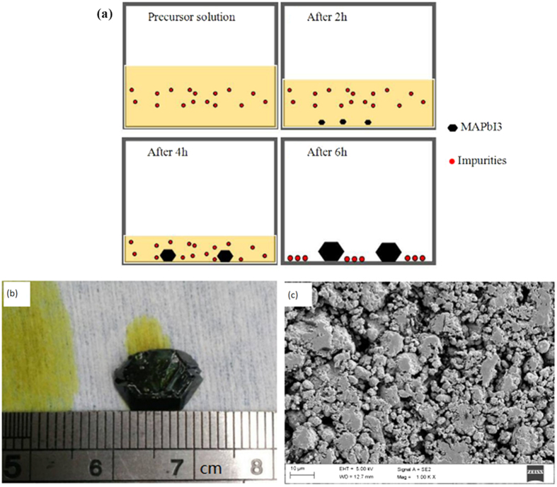
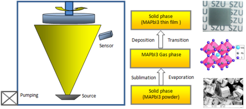
As shown in Fig. 1(a), the MAPbI3 crystal was grown by maintaining the precursor solution at 90 °C on the hot plate so that a high-quality MAPbI3 crystal with fewer impurities was obtained after some hours (Fig. 1(b)). The raw MAPbI3 crystal with fewer impurities is favourable for the prepared MAPbI3 thin film and solar cells. To easily evaporate MAPbI3, the MAPbI3 crystals were ground to small crystals or powder before use (Fig. 1(c)). As shown in Fig. 2, with the single-source physical vapour-deposition (SSPVD) method, the work current of the crucible was rapidly increased from 0 A to 100 A, and simultaneously, the temperature of the source was rapidly raised to the point at which the MAPbI3 powder either evaporates or sublimates efficiently without a chemical reaction; the MAPbI3 powder is then converted to the MAPbI3 gas phase by evaporation and the film is deposited on the substrates atomistically. The entire deposition process, conversion to the gas phase, and movement and condensation to the substrate, was such that only the physical morphology of the aggregate state of the material changes from solid to gaseous and back to solid. However, chemically, the MAPbI3 material remains the same. With this SSPVD method, MAPbI3 gases are guided to the substrate without undergoing a chemical reaction on the way to the substrate. Then, nucleation and crystallization of the MAPbI3 thin film on the substrate was facilitated by the mere effect of the removal of the gas phase of MAPbI3. Therefore, the use of subsequent thermal annealing treatment to evaporate the solvent or crystallize the perovskite film is unnecessary. Owing to the advantages of the single-source physical vapour-deposition process without reaction, this method is a facile and attractive approach for the fabrication of high-quality perovskite films.
Figure 1.
Progress of the MAPbI3 crystal growth (a), photos of MAPbI3 crystal (b) and MAPbI3 powder (c).
Figure 2. Single-source physical vapour-deposition process of the perovskite MAPbI3 thin film.
X-ray diffraction (XRD) measurements were used to further examine the formation of perovskite phases and crystallization. As shown in Fig. 3(a), a set of preferred orientations at 14.08°, 28.44°, 31.85°, 40.58° and 43.19° was observed, with these assigned to the (110), (220), (310), (224) and (330) planes of the MAPbI3 perovskite tetragonal structure33, respectively. Minor peaks of the (200), (211), (202), (312), (404) and (226) planes are present at 2θ values of 19.92°, 23.54°, 24.52°, 34.94°, 50.22°, and 52.54°, respectively, clearly indicating that all perovskite films or powder are of high phase purity. Furthermore, there are no MAI or PbI2 phase peaks in the powder or the film, confirming that the samples are also compositionally pure. Notably, the spectrum of the single-source physical vapour-deposited perovskite film is similar to the spectrum of the source of the perovskite powder, confirming that the film and powder consist of the same MAPbI3 material. Furthermore, owing to the change of the material in physical morphology from the MAPbI3 crystal to the MAPbI3 thin film, the perovskite film peaks became more intense. All analyses clearly indicate that the conversion of the MAPbI3 crystal to the MAPbI3 thin film only changes the physical morphology during the single-source physical vapour-deposition process, without undergoing a chemical decomposition. These findings are further supported by the EDS spectral line pattern and elemental composition.
Figure 3.
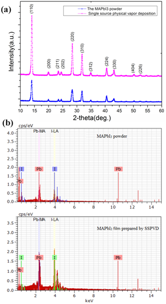
XRD patterns of MAPbI3 powder and film prepared by SSPVD (a), EDS spectral line pattern of MAPbI3 powder and film prepared by SSPVD (b).
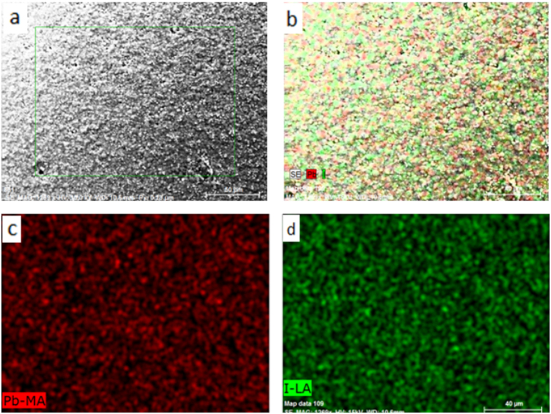
The EDS technique was used to analyse the composition and element ratio of the MAPbI3 powder and the MAPbI3 film prepared by SSPVD. As shown in Fig. 3(b), there are two feature peaks at 2.48 and 3.98 keV, which are assigned to the Pb and I elements, respectively. The EDS spectral line pattern of the perovskite film is similar to the spectrum of the source perovskite powder, clearly indicating their homogeneity. The similar value of approximately 0.339 and 0.334 are obtained for the Pb/I ratio of the film grown via single-source physical vapour-deposition and for the MAPbI3 powder, respectively. Both values are close to the theoretical stoichiometry value of 0.333, confirming that the perovskite film prepared by SSPVD has the same composition as the MAPbI3 powder. These findings are supported by the XRD analysis results discussed above. Furthermore, examination of the EDS-Mapping presented in Fig. 4 shows that Pb and I are well distributed on a large scale, confirming the uniformity of the MAPbI3 film grown via the SSPVD method.
Figure 4.
SEM-BSD morphologies (a) and EDS-Mapping of the MAPbI3 film (the combination map of the Pb and I (b), Pb (c) and I (d).
As can be clearly observed in Fig. 5, the films prepared by single-source physical vapour-deposition are extremely dense, compact and uniform even on a large scale as shown in the low-magnification SEM image (Fig. 5(a)), indicating that this method will be suitable for fabricating high-quality perovskite solar cells over a large area. At the same time, the high-resolution SEM image (Fig. 5(b)) reveals that the as-deposited perovskite films without the subsequent thermal annealing treatment also possess the characteristics of full surface coverage on the substrates without pinholes but with remarkable grain size of up to 2 μm, indicating a higher level of crystallization compared with the dual-source vapour-evaporation processed films. The uniform, smooth, nonporous and complete surface coverage of the perovskite thin film without heat-treating suggests that these films are promising for applications in flexible solar cells. These results confirm the progress of the nucleation and crystallization of MAPbI3 from the gas phase to the thin film without the need of subsequent thermal annealing treatment. These impressive characteristics could be due to the ability to easily control the evaporation rate, time, and pressure with high reproducibility in the single-source physical vapour-deposition process without reaction.
Figure 5.
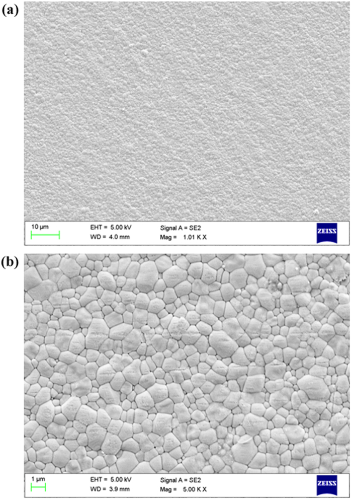
SEM images of MAPbI3 thin films (low-magnification SEM image (a) and high-magnification SEM image (b)).
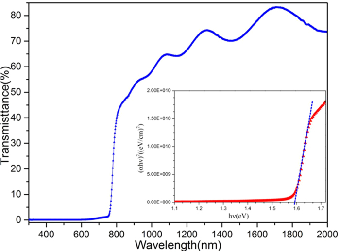
Figure 6 shows the transmittance spectra as a function of wavelength for the MAPbI3 film prepared by the single-source physical vapour-deposition method. The transmittance of the MAPbI3 film changed from 80% to 49% slowly in the wavelength span from 2000 nm to 800 nm. However, the transmittance decreased drastically at 800 nm, confirming the existence of a sharp absorption edge11. Last, the transmittance was low and close to 0% in the wavelength range from 765 nm to 350 nm, indicating that good crystallinity of the MAPbI3 films was obtained, making this material a good light-absorber over the entire visible solar emission spectrum. Additionally, the band gap energy was calculated according to
Figure 6. Transmitted spectrum and the optical band gap estimation (insert) of MAPbI3 thin film.
 |
where α is the absorption coefficient, hv is the photon energy, A is a constant, and E is the band gap energy. As shown in Fig. 6, the results revealed that the band gap of the MAPbI3 thin film is approximately 1.59 eV, which is close to the theoretical value of 1.55 eV reported by Baikie11.
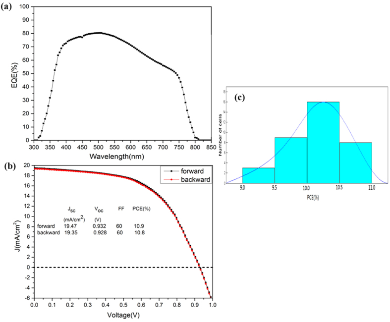
Figure 7(a) shows that the EQE rises at the same wavelength, reaching a maximum value of 80.1% in the 475–525 nm wavelength range. The current density-voltage (J-V) characteristics of the solar cell based on the best performing device reported in Fig. 7(b) exhibited a JSC of 19.47 mA/cm2, a FF of 60%, and a VOC of 0.932 V, leading to a high PCE of 10.9%. The J-V curve is almost independent of the scan direction, indicating that no obvious photocurrent hysteresis occurred. The observed small reduction may be due to the high humidity present in the test environment (approximately 60–78%). The statistics for the PCE based on 36 devices are shown in Fig. 7(c). The figure shows that a narrow distribution of PCE values in the 9.0–11.0% range with the average value of 10.2 ± 0.1% was obtained. The improved reproducibility in device performance is closely related to the reproducibility of MAPbI3 films prepared by SSPVD.
Figure 7.
External quantum efficiency spectra for the best perovskite solar cell (a), J-V characteristic curve (b) and PCE histograms of MAPbI3 thin film solar cells (c).
Conclusion
In summary, we report SSPVD, a facile, efficient and reproducible method for the fabrication of perovskite thin films. This method involves the process of converting the MAPbI3 powder to the gas phase, transferring the MAPbI3 gas to the samples and then condensing the MAPbI3 gas onto the surface of the substrates.During this process only the physical morphology of the aggregate state of the material changes, which is different from the methods reported that are based on the reaction process between the organic and inorganic sources. A perovskite thin film with uniform, smooth, nonporous and complete surface coverage as well as with a high level of phase purity and good crystallization was formed via SSPVD. The initial results for the device show that a PCE of approximately 10.90% was obtained for MAPbI3 grown by SSPVD, suggesting that this method is promising for further significant optimization and application in larger surface area perovskite MAPbI3 solar cells with higher PCEs.
Methods
Material preparation
CH3NH3I synthesis: first, methylammonium iodide (MAI) was synthesized by reacting hydroiodic acid (HI) (60 ml, 57 wt% in water, Sigma Aldrich) and methylamine (CH3NH2) (56 ml, 40 wt% in water, Sigma Aldrich) in a 250 ml round bottom flask at 0 °C for 2 h with constant magnetic stirring. Second, the white methylammonium iodide powder was crystallized by evaporating solvents at 90 °C for 2 h. Then, the crystallized white methylammonium iodide powder was purified with diethyl ether three times. Subsequently, methylammonium iodide was dried at 60 °C in vacuum overnight. Finally, the white methylammonium iodide powder was saved at 25 °C in a vacuum oven and was desiccated before use.
Preparation of the precursor solution and MAPbI3 crystal: To generate the perovskite solution, CH3NH3I (0.8 g) and PbI2 (2.3 g, 99.99%, Sigma Aldrich) were dissolved in r-butyrolactone (100 ml, 99%, Sigma Aldrich) in a 250 ml MAPbI3 round bottom flask at 60 °C for 10 h with constant magnetic stirring. Then, the MAPbI3 precursor solution was maintained at 90 °C on the hot plate. After 2 h, there were many small seed crystals grown with solvent evaporating as the same time. Then, the two largest seed crystals were kept to grow, and others were discarded. The above step was repeated until all precursor solution was evaporated. Finally, the MAPbI3 crystals were ground to powder before use.
Film preparation
Single-source physical vapour-deposition method: K9 glass substrates with the thickness of approximately 1 mm were ultrasonically cleaned in acetone, alcohol and deionized water, sequentially. Then, 0.6 g of MAPbI3 powder was placed into a crucible. When the pressure in the chamber was pumped down to below 1 × 10⁻³ Pa, the work current of the crucible was rapidly increased from 0 A to 100 A, and at the same time, the temperature of source was raised rapidly to the point at which the MAPbI3 powder either evaporates or sublimates efficiently. The value of the deposition rate of the thin film on the sensor was approximately 8.5 ± 1.3 Å/s. There is a close relationship between the power and the rate of deposition. The total process of the deposition was approximately 3 min and then the sample shutter was closed. The value of the thickness of the thin film on the sensor was approximately 8.9 kÅ. As the same time, the substrate holder was rotated at a rate of 5 rpm to ensure uniform evaporation. The actual deposited equivalent thickness was approximately 400 nm.
Device fabrication
ITO-coated glass substrates (10 Ohm/sq, YINKOU OPVTECH) were cleaned with ethyl alcohol and deionized water in a sonicator for 15 min each. Then, the cleaned substrates were treated by oxygen plasma for 30 min. A thin layer of PEDOT:PSS (CLEVIOS PVP AI4083,80 nm) was fabricated by spin-coating, followed by annealing at 120 °C on a hot plate for 15 min. A perovskite layer was deposited on top of the PEDOT:PSS layer via the SSPVD method. A PCBM solution (10 mg in 1 ml chlorobenzene, 100 nm) was spun on the prepared perovskite film. Finally, 80 nm thick Ag electrodes were deposited using a thermal evaporator. The vapour pressure was 1 × 10⁻³ Pa inside the vacuum chamber and the value of the Ag deposition rate on the sensor was approximately 12 Å/s.
Characterization
SEM
The perovskite film morphology was analysed using a SUPRA 55 scanning electron microscope (SEM) using an electron beam accelerated at 5 kV.
EDS
The composition and element mapping of films and perovskite powder were obtained using an energy dispersive X-ray microanalysis system (Model: BRUKER QUANTAX 200) attached to the SEM.
XRD
Crystallographic structures of films were analysed by X-Ray diffraction (XRD) technique (Ultima IV) with CuKα radiation (0.15406 nm) operated at 40 kV and 40 mA using  /2
/2 scans, whereas perovskite powder was analysed using 2
 scans.
Optical transmittance
Optical transmittance properties of the perovskite films were obtained using an ultraviolet (UV)/visible (VIS)/near-infrared (NIR) spectrophotometer (Lambda 950, Perkin Elmer).
Film thickness
The prepared film thickness was measured using a DEKTAK XT profilometer.
Devices measurement
The solar cells were tested in air, the temperature was approximately 27 °C, and the humidity was between 65% and 75%. The current density-voltage (J-V) characteristics of the perovskite cells were measured under simulated AM 1.5G conditions (100 mW/cm2) with a Keithley 2400. The voltage was scanned from 0 V(1 V) to 1 V(0 V) with the scan rate of approximately 0.1 V/s. The active area was approximately 9 mm2. The EQE spectra were acquired under 1.5 AM white light using an EQE 200 Oriel integrated system. The measurement step was 10 nm and the photocurrent was recorded using a lock-in amplifier.
Additional Information
How to cite this article: Fan, P. et al. High-performance perovskite CH3NH3PbI3 thin films for solar cells prepared by single-source physical vapour deposition. Sci. Rep. 6, 29910; doi: 10.1038/srep29910 (2016).
Acknowledgments
This work was supported by National Natural Science Foundation of China (Grant No. 61404086). Basical Research Program of Shenzhen (JCYJ20150324140036866) and the special fund of the central finance for the development of local Universities (Grant No. 000022070150).
Footnotes
Author Contributions P.F. and G.-X.L. designed and conducted the project. D.G. conducted the experiments. The data analyses were performed by P.F. and G.-X.L. This manuscript was written by D.G. J.-T.L., D.-P.Z., Z.-H.Z. and J.L.C. participated in the discussion. All authors reviewed this manuscript.
References
- Sum T. C. & Mathews N. Advancements in perovskite solar cells: photophysics behind the photovoltaics. Energy Environ. Sci. 7, 2518–2534 (2014). [Google Scholar]
- Brenner T. M., Egger D. A., Kronik L., Hodes G. & Cahen D. Hybrid organic—inorganic perovskites: low-cost semiconductors with intriguing charge-transport properties. Nat. Rev. Mater. 1, 15007 (2016). [Google Scholar]
- Green M. A., Ho-Baillie A. & Snaith H. J. The emergence of perovskite solar cells. Nat. Photonics 8, 506–514 (2014). [Google Scholar]
- Rong Y., Liu L., Mei A., Li X. & Han H. Beyond Efficiency: the Challenge of Stability in Mesoscopic Perovskite Solar Cells. Adv. Energ. Mater. 5, n/a–n/a (2015). [Google Scholar]
- Kojima A., Teshima K., Shirai Y. & Miyasaka T. Organometal Halide Perovskites as Visible-Light Sensitizers for Photovoltaic Cells. J. Am. Chem. Soc. 131, 6050–6051 (2009). [DOI] [PubMed] [Google Scholar]
- Bi D. et al. Efficient luminescent solar cells based on tailored mixed-cation perovskites. Sci. Adv. 2, e1501170 (2016). [DOI] [PMC free article] [PubMed] [Google Scholar]
- Xing G. et al. Long-range balanced electron- and hole-transport lengths in organic-inorganic CH3NH3PbI3. Science 342, 344–347 (2013). [DOI] [PubMed] [Google Scholar]
- Stranks S. D. et al. Electron-hole diffusion lengths exceeding 1 micrometer in an organometal trihalide perovskite absorber. Science 342, 341–344 (2013). [DOI] [PubMed] [Google Scholar]
- Shi D. et al. Low trap-state density and long carrier diffusion in organolead trihalide perovskite single crystals. Science 347, 519–522 (2015). [DOI] [PubMed] [Google Scholar]
- Dong Q. et al. Electron-hole diffusion lengths >175 mum in solution-grown CH3NH3PbI3 single crystals. Science 347, 967–970 (2015). [DOI] [PubMed] [Google Scholar]
- Baikie T. et al. Synthesis and crystal chemistry of the hybrid perovskite (CH3NH3)PbI3 for solid-state sensitised solar cell applications. J. Mater. Chem. A 1, 5628 (2013). [Google Scholar]
- Zhou H. et al. Interface engineering of highly efficient perovskite solar cells. Science 345, 542–546 (2014). [DOI] [PubMed] [Google Scholar]
- Nie W. et al. High-efficiency solution-processed perovskite solar cells with millimeter-scale grains. Science 347, 522–525 (2015). [DOI] [PubMed] [Google Scholar]
- Lee M. M., Teuscher J., Miyasaka T., Murakami T. N. & Snaith H. J. Efficient hybrid solar cells based on meso-superstructured organometal halide perovskites. Science 338, 643–647 (2012). [DOI] [PubMed] [Google Scholar]
- Kim H. S. et al. Lead iodide perovskite sensitized all-solid-state submicron thin film mesoscopic solar cell with efficiency exceeding 9%. Sci. Rep. 2, 591 (2012). [DOI] [PMC free article] [PubMed] [Google Scholar]
- Carnie M. J. et al. A one-step low temperature processing route for organolead halide perovskite solar cells. Chem. Commun. 49, 7893–7895 (2013). [DOI] [PubMed] [Google Scholar]
- Burschka J. et al. Sequential deposition as a route to high-performance perovskite-sensitized solar cells. Nature 499, 316–319 (2013). [DOI] [PubMed] [Google Scholar]
- Dualeh A. et al. Effect of Annealing Temperature on Film Morphology of Organic-Inorganic Hybrid Pervoskite Solid-State Solar Cells. Adv. Funct. Mater. 24, 3250–3258 (2014). [Google Scholar]
- Chen Y., Chen T. & Dai L. Layer-by-layer growth of CH(3)NH(3)PbI(3-x)Clx for highly efficient planar heterojunction perovskite solar cells. Adv. Mater. 27, 1053–1059 (2015). [DOI] [PubMed] [Google Scholar]
- Chen Q. et al. Planar heterojunction perovskite solar cells via vapor-assisted solution process. J. Am. Chem. Soc. 136, 622–625 (2014). [DOI] [PubMed] [Google Scholar]
- Liu M., Johnston M. B. & Snaith H. J. Efficient planar heterojunction perovskite solar cells by vapour deposition. Nature 501, 395–398 (2013). [DOI] [PubMed] [Google Scholar]
- Ng A. et al. Efficiency enhancement by defect engineering in perovskite photovoltaic cells prepared using evaporated PbI2/CH3NH3I multilayers. J. Mater. Chem. A (2015). [Google Scholar]
- Ono L. K., Wang S., Kato Y., Raga S. R. & Qi Y. Fabrication of semi-transparent perovskite films with centimeter-scale superior uniformity by the hybrid deposition method. Energy Environ. Sci. 7, 3989–3993 (2014). [Google Scholar]
- Chen C. W. et al. Efficient and uniform planar-type perovskite solar cells by simple sequential vacuum deposition. Adv. Mater. 26, 6647–6652 (2014). [DOI] [PubMed] [Google Scholar]
- Aldibaja F. K. et al. Effect of different lead precursors on perovskite solar cell performance and stability. J. Mater. Chem. A 3, 9194–9200 (2015). [Google Scholar]
- Wu Y. et al. Retarding the crystallization of PbI2for highly reproducible planar-structured perovskite solar cells via sequential deposition. Energy Environ. Sci. 7, 2934 (2014). [Google Scholar]
- Wakamiya A. et al. Reproducible Fabrication of Efficient Perovskite-based Solar Cells: X-ray Crystallographic Studies on the Formation of CH3NH3PbI3 Layers. Chem. Lett. 43, 711–713 (2014). [Google Scholar]
- Zhao Y. Q. et al. Tuning superior solar cell performance of carrier mobility and absorption in perovskite CH3NH3GeCl3: A density functional calculations. J. Power Sources 313, 96–103 (2016). [Google Scholar]
- Kadro J. M., Nonomura K., Gachet D., Gratzel M. & Hagfeldt A. Facile route to freestanding CH3NH3PbI3 crystals using inverse solubility. Sci. Rep. 5, 11654 (2015). [DOI] [PMC free article] [PubMed] [Google Scholar]
- Liu Y. et al. Two-Inch-Sized Perovskite CH3 NH3 PbX3 (X = Cl, Br, I) Crystals: Growth and Characterization. Adv. Mater. 27, 5176–5183 (2015). [DOI] [PubMed] [Google Scholar]
- Dualeh A., Gao P., Seok S. I., Nazeeruddin M. K. & Grätzel M. Thermal Behavior of Methylammonium Lead-Trihalide Perovskite Photovoltaic Light Harvesters. Chem. Mater. 26, 6160–6164 (2014). [Google Scholar]
- Zhang W. et al. Ultrasmooth organic-inorganic perovskite thin-film formation and crystallization for efficient planar heterojunction solar cells. Nat Commun 6, 6142 (2015). [DOI] [PubMed] [Google Scholar]
- D. B. Templating and structural engineering in organic-inorganic perovskites. J. Chem. Society-Dalton Transactions 1, 1–12 (2001). [Google Scholar]


