

Abstract
We demonstrate arrays of opioid biosensors based on chemical vapor deposition grown molybdenum disulfide (MoS2) field effect transistors (FETs) coupled to a computationally redesigned, water-soluble variant of the μ-opioid receptor (MOR). By transferring dense films of monolayer MoS2 crystals onto prefabricated electrode arrays, we obtain high-quality FETs with clean surfaces that allow for reproducible protein attachment. The fabrication yield of MoS2 FETs and biosensors exceeds 95%, with an average mobility of 2.0 cm2 V−1 s−1 (36 cm2 V−1 s−1) at room temperature under ambient (in vacuo). An atomic length nickel-mediated linker chemistry enables target binding events that occur very close to the MoS2 surface to maximize sensitivity. The biosensor response calibration curve for a synthetic opioid peptide known to bind to the wild-type MOR indicates binding affinity that matches values determined using traditional techniques and a limit of detection ~3 nM (1.5 ng/mL). The combination of scalable array fabrication and rapid, precise binding readout enabled by the MoS2 transistor offers the prospect of a solid-state drug testing platform for rapid readout of the interactions between novel drugs and their intended protein targets.
Keywords: transition-metal dichalcogenide, monolayer MoS2, biosensors, scalable, opioids
Graphical abstract
Nanomaterials such as carbon nanotubes and graphene hold great promise for biosensing applications due to their environmentally sensitive electronic properties and all-surface geometries that result in enhanced sensitivity to target binding events.1 Nanomaterial–protein hybrid devices have been shown to be sensitive to conformational changes of a single protein,2 and nanobio hybrid devices have been used to detect cancer biomarker proteins3 and other small molecule targets4 at femtomolar concentrations. It has been suggested that two-dimensional materials that are intrinsic semiconductors with an energy band gap (e.g., MoS2) may exhibit better performance than graphene for this application.5,6 However, reproducible, high-yield fabrication processes are necessary for this emerging technology.
Approaches have been established to couple proteins to nanomaterials by linker chemistries that target exposed amino acid residues. For example, amine sites are common on the exterior of proteins, which enables chemistries that link carbon nanotubes or graphene to almost any protein via amide bond formation.7–9 However, in order to increase device-to-device reproducibility and lower detection thresholds, linker chemistries that provide control over the site of the chemical bond to the protein can be beneficial. In particular, polyhistidine tags (histags), which are routinely used to enable purification of recombinant proteins, have been targeted for this purpose.10–13
Here, we present an approach to fabrication of large arrays of biosensors based on field effect transistors (FETs) derived from molybdenum disulfide (MoS2) grown by chemical vapor deposition (CVD). We introduce a nickel ion mediated surface functionalization scheme for attachment of recombinant proteins via a histidine tag directly to the MoS2 surface, without the need for deposition of an oxide layer on top of the FET channel.5 The linker chemistry is compact, ensuring that target binding events occur close to the MoS2 surface. Since signal transduction in FET biosensors is dominated by electrostatic interactions,14 this should lead to enhanced sensitivity, especially in ionic solutions (e.g., bodily fluids) where the Debye length can be on the scale of a few nanometers.15–18 The biosensors used here are based on a computationally redesigned water-soluble variant of the human μ-opioid receptor (MOR), referred to as wsMOR, which has structural properties similar to those of the wild-type receptor and comparable opioid affinities.19,20 The wsMOR–MoS2 biosensors are used to read out the binding of DAMGO ([D-Ala2, N-MePhe4, Gly-ol]-enkephalin), a synthetic opioid peptide with high specificity for the native MOR. The wsMOR affinity inferred from the biosensor data agrees with results for the native MOR based on conventional analytical techniques. The array fabrication method outlined here is scalable, yielding sensitive devices that provide quick, accurate readouts of receptor binding. The work opens a path toward multiplexed arrays of MoS2-based biosensors for many applications, for example, a drug-testing platform that would allow for rapid readout of the interactions between novel drugs and their intended protein target in a solid-state test bed.
RESULTS AND DISCUSSION
Recently developed methods for CVD growth of monolayer MoS221–23 offer prospects for devices and systems beyond the exploratory work enabled by mechanical microexfoliation.15,16 Indeed, due to the small size and low areal density of monolayer flakes achieved through microexfoliation, a reliable large-area growth process for dense monolayer MoS2 flakes is essential for scalable fabrication. In a typical CVD process, sulfur sublimated from a solid source is introduced into the furnace along with a molybdenum source such as molybdenum oxide24,25 or ammonia heptamolybdate,26 and triangular monolayer flakes of MoS2 nucleate and grow directly on the substrate. Although the mobility of MoS2, typically 1–50 cm2 V−1 s−1,23,27,28 is lower than that of graphene, the presence of a 1.8 eV direct bandgap for monolayer MoS229 provides the devices with on/off ratios as large as 10723,27 and strong photoluminescence.26,30,31 These properties make MoS2 promising for photonic and optoelectronic applications including vapor sensors,32,33 solar cells,34,35 optical modulators, 36,37 and valleytronics.38
For these experiments, MoS2 samples were grown via CVD in a 1 in. quartz tube furnace (Figure 1a). Microliter droplets of saturated ammonia heptamolybdate solution were dried onto the corners of a 2 cm × 8 cm Si/SiO2 growth substrate that had previously been coated with a layer of sodium cholate (1% solution spin coated 4000 rpm for 60 s). Sodium cholate is a known growth promoter, acting to increase diffusion of the molybdenum source by increasing the surface adhesive energy relative to the adatom cohesive energy.26 The growth substrate was placed in the center of the furnace and heated to 800 °C at a rate of 70 °C min−1. A 25-mg sulfur pellet was placed on a piece of silicon and positioned upstream in the furnace at a distance of 16 cm from the growth substrate, such that its temperature was approximately 150 °C, sufficient for the pellet to melt and evaporate slowly. A flow of 500 sccm N2 carried the sulfur vapor into the furnace during a 30 min growth period. After growth, the sample was rapidly cooled by cracking open the furnace and sliding it downstream with respect to the 1 in. quartz tube.
Figure 1.

MoS2 growth and devices. (a) Schematic of the CVD growth setup. (b) Photograph of the electrode array chip onto which MoS2 is transferred. Each of the 10 columns of contact pads leads to a cluster of interdigitated electrodes, one of which is shown in panel c. (c) Optical micrograph showing interdigitated electrodes corresponding to a set of 10 sensors. The dark purple regions are monolayer MoS2. (d) Higher magnification optical micrograph showing how multiple triangular, crystalline monolayer MoS2 flakes span the electrodes.
The growth process leaves the Si/SiO2 surface decorated with triangular crystals of monolayer MoS2. The sensor array fabrication process is designed to minimize the need for lithography and etching steps that can contaminate and degrade the samples. To that end, we transferred the randomly grown MoS2 flakes onto prefabricated electrodes by releasing the samples from the growth substrate with a polymer backing layer.21 This was accomplished by spin-coating PMMA onto the sample, which was then placed in a bath of 0.1 M KOH to slowly etch the SiO2 surface and release the PMMA/MoS2 layer from the substrate. The floating PMMA/MoS2 layer was then transferred into successive water baths for cleaning and finally scooped onto a target substrate that had prefabricated arrays of metal contacts, defined using photolithography (Figure 1b–d). The sample was dried, and the PMMA was removed with an acetone spray, followed by an acetone bath. The electrode design used individual source fingers, interdigitated with a common drain electrode. The effective device area of 10 μm (channel length) × 2 mm (channel width) ensured that many MoS2 flakes spanned each electrode pair, leading to a device yield exceeding 90% and good reproducibility of device electrical properties (see below). Each die contained 100 devices, arranged as 10 sets of 10 devices, where each set could be addressed independently for chemical functionalization and testing of analyte responses (Figure 1c).
The material was characterized after transfer by aberration corrected TEM (ACTEM), atomic force microscopy (AFM), and Raman spectroscopy. ACTEM showed the expected hexagonal lattice, with different brightness levels for the molybdenum and sulfur sites reflecting their different atomic numbers (Figure 2a,b). AFM (Figure 2e) revealed that the film was clean and uniform with thickness ~0.8 nm, consistent with monolayer MoS2.39 Raman spectroscopy showed the expected E2g and A1g MoS2 intraband vibrational modes, separated by 19 cm−1 (Figure 2d),39,40 as expected for monolayer MoS2.33,34 Together, these experiments confirm that the MoS2 samples are highly crystalline with very high monolayer content.
Figure 2.

Physical characterization of MoS2. (a) Aberration-corrected TEM image shows the honeycomb lattice expected for MoS2. (b) Higher magnification image shows brightness differences for the Mo and S sites. (c) Ball-and-stick model for monolayer MoS2, consistent with the TEM data in panels a and b. (d) Raman spectrum of the MoS2 film shows positions and separation of the E2g and A1g Raman peaks consistent with monolayer MoS2. (e) AFM topographic image reveals a pristine surface, 0.8 nm in height before functionalization. (f) AFM topographic image after functionalization shows dense coverage with 2–3 nm high features, consistent with coverage of proteins bound with the Ni2+–histidine linker.
Current-back gate voltage (I–Vg) measurements conducted under ambient conditions showed the expected n-type behavior of MoS2, with hysteresis ascribed to adsorbed water41 and substrate charge traps.42 Figure 3a shows the I–Vg of a device composed of ~15 individual MoS2 crystalline flakes. By summing the active area of the individual crystals that span the electrodes to derive the effective length and width of the channel, we estimate the field effect mobility to be 1.9 cm2/V-s. Measurements in vacuo, however, showed greatly increased conductivity and inferred field effect mobility. Across a set of 18 devices measured under ambient and then again at a pressure of 10−6 Torr, the average mobility increased from 1.2 cm2/V-s to 36 cm2/V-s, while the on-state current increased by a factor of approximately 50 (data not shown). This enhancement is ascribed to removal of atmospheric adsorbates that suppress conduction through the MoS2 and/or limit the mechanical contact between the MoS2 and the underlying electrodes. Figure 3b shows I–Vg curves for 70 devices on a single chip, measured under ambient. The yield is over 95% (68/70 functioning devices), and device properties are highly reproducible once the curves are normalized by their respective on-state currents (Figure 3c). Based on this observation, differences in on-state currents across devices are assumed to reflect primarily variation in the number of MoS2 flakes spanning the electrodes. A histogram of threshold voltages shows a tight distribution, with ~75% of the devices having a turn-on voltage in the range –16 to –10 V.
Figure 3.

Electrical characteristics of MoS2 devices. (a) Typical I–Vg characteristic, showing on/off ratios as large as 106 and device hysteresis, ascribed to surface charge injection. (b) I–Vg characteristics for 70 devices in an array measured under ambient conditions. (c) Curves from panel b normalized to the on-state current. The collapse of the data suggests that device variation is due primarily to variation in the number of MoS2 flakes contacted. (d) Histogram of turn-on voltages for a set of 70 devices.
Previous studies43,44 of MoS2-based biosensors have utilized a top dielectric layer as the binding surface for protein functionalization. Disadvantages of this approach include fabrication complexity and the fact that the target-binding event is necessarily remote from the transistor channel, which is expected to reduce the sensitivity of the device. Here, we instead relied upon direct binding of the protein to the MoS2 using nickel ions that bind to the histidine tag of the recombinant protein as a well-defined anchoring site. A similar surface functionalization approach was previously used to attach ligands to MoS2 nanoparticles in order to alter their solubility.45 The protein functionalization process begins by incubating the MoS2 FET array in 5 mM NiCl2 solution so that Ni2+ ions form coordinate covalent bonds with a trio of sulfur atoms in the top layer of the MoS2. These ions are then available to bind to nickel-chelating agents, such as histidine residues,12,13 nitrilotriacetic acid,12 ethylenediamines,46 or nickel porphyrins.47 The resulting MoS2–protein hybrid structure is shown schematically in Figure 4b,c. The histidine tag has been used as an anchor site in other biosensor systems, including those based on carbon nanotube12 and graphene13 FETs. These previous functionalization schemes relied upon nitrilotriacetic acid to bind Ni ions, resulting in a ~2 nm thick linker layer.13 The MoS2 functionalization scheme presented here is a simple, one-step surface chemistry that results in an extremely short linker. This is expected to ensure strong electrostatic coupling of target binding events to the MoS2 channel and should render the devices robust against screening that occurs for measurements in ionic liquids.
Figure 4.

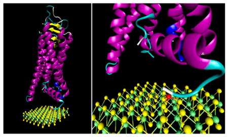
MoS2 structure and functionalization schematic. Sulfur atoms are shown in yellow, molybdenum in green. The nickel ion used as a protein linker is shown in red. The MOR protein is made of seven connected α-helices and C-terminus and N-terminus tails that contribute to the protein function. The histidine tag region is shown in white.
Experiments were based upon a computationally redesigned, water-soluble variant of the human μ-opioid receptor (MOR),19,20 referred to as wsMOR. The redesigned variant of the MOR used in this experiment was expressed in E. coli and purified using standard techniques,19 without the need for a membrane or membrane surrogate such as a nanodisk.12,48 Physiologically, the native MOR is involved in pain and reward recognition pathways, and it has high affinity for endogenous and exogenous opioids such as heroin, morphine, β-endorphin, enkephalin, and β-funaltrexamine. The wsMOR has been previously used in a graphene biosensor construct where its affinity for the drug target naltrexone was confirmed.4 For this work we used a different target [D-Ala2, N-MePhe4, Gly-ol]-enkephaline (Sigma-Aldrich), DAMGO, the synthetic opioid peptide analogue to enkephalin. Natural enkephalins are endogenous opioid pentapeptides involved in pain perception, cognitive functions, affective behaviors, and locomotion.49 Experiments were based on solutions of DAMGO diluted in deionized water to concentrations in the picomolar to micromolar range.
AFM was used to examine the surface morphology of the same MoS2 flake before and after protein attachment. Before functionalization, the surface of the flake was uniform and nearly featureless (Figure 2e). After chemical treatment based on a 10 μM solution of wsMOR, AFM revealed a nearly uniform layer of 2–3 nm high features (density ~330/μm2), consistent with the size of the 46 kDa wsMOR (Figure 2f). The SiO2 surface remained very smooth, indicating that wsMOR does not adsorb nonspecifically on the surface but instead is preferentially bound to Ni ions on the MoS2.
After wsMOR attachment, the device on-state conductance typically dropped by ~70% (Figure 5a), attributed to depletion of electron carriers due to the binding chemistry and increased carrier scattering due to the presence of the Ni2+ ions and bound wsMOR. The devices were then exposed to the target DAMGO in deionized (DI) water. On the basis of the trends in the data (Figure 5a), the sensor response is reported as the percent increase in on-state current (upper branch of the I–Vg characteristic) at Vg = 0 V, measured before and after the introduction of the target DAMGO. The response-vs-concentration curve shows a sigmoidal shape that is well fit by a model based on the Langmuir–Hill equation for ligand–receptor binding at equilibrium
Figure 5.

Electrical signatures of protein-target binding. (a) Current–gate voltage characteristics of an as-fabricated FET, the FET biosensor after wsMOR functionalization, and the biosensor after exposure to the target DAMGO. The biosensor conductivity increases upon exposure to DAMGO, which is taken as the sensor response. (b) Response versus concentration characteristic for the biosensor (red markers) and negative control experiment where the wsMOR functionalization step was omitted (blue markers). The biosensor calibration curve is well described by a model based upon the Langmuir–Hill isotherm (red curve). The error bars represent the standard deviation of the mean.
where C is the DAMGO concentration, A is the response when all binding sites are occupied, Ka is the concentration that yields half the maximum response, Z is an offset response to pure water, and n is the Hill coefficient, describing cooperativity and other effects. For this data set, A = 117 ± 17%, Ka = 87 ± 39 nM, and n = 0.87 ± 0.23, and Z = –23 ± 4%. A Hill coefficient near n = 1 suggests noncooperative binding for this system. From standard measurements performed by others,50 DAMGO is known to bind to the wild-type MOR with an affinity in the range of tens of nanomoles, consistent with the value found through the fitting procedure. The close agreement between our results and affinity measurements from more traditional techniques demonstrates that the affinity of the reengineered membrane protein for this target is comparable to that of the wild type and that this chemical recognition functionality is retained after surface immobilization, enabling sensitive, rapid readout of the target concentration with this device construct. We performed a negative control experiment to test whether DAMGO is exclusively reacting with the wsMOR. In the control experiment the wsMOR functionalization step was omitted, and MoS2 FET devices were tested against DAMGO solutions at various concentrations as described in the Methods. The measured responses were identical for all DAMGO concentrations tested and statistically indistinguishable from biosensor responses to pure DI water (Figure 5b). This negative control experiment demonstrates that specific binding of DAMGO to the wsMOR is essential for the observed sensor responses.
CONCLUSIONS
In summary, we have demonstrated wafer-scale, high-yield fabrication of monolayer MoS2-based biosensors based upon CVD growth and direct protein functionalization of the MoS2 surface. The chemical recognition functionality of the computationally redesigned receptor protein is retained when it is immobilized and read out electronically, and the inferred binding affinity is comparable to that found using other measurement techniques. The combination of this reproducible, high-yield fabrication method and versatile linker chemistry should be suitable for the construction of multiplexed biosensor arrays appropriate for simultaneous detection of multiple targets in complex fluids. With further understanding of the relationship between conformational changes induced by target binding and sensor output signals, this approach might also enable construction of a solid-state device useful for understanding the interactions between other molecular targets and novel engineered receptor variants.
EXPERIMENTAL METHODS
Raman Spectroscopy
Raman spectroscopy was conducted on MoS2 monolayer films directly after growth. Raman spectra were acquired using an ND–MDT system under ambient conditions with and excitation wavelength of 532 nm. The laser power was set to 2 mW to avoid sample heating and/or degradation of the MoS2. All the spectra were consistent with monolayer MoS2, with minimal bilayer content (<5%).
Fabrication of Field-Effect Transistor Arrays
Fabrication of FET arrays is based upon traditional photolithography methods. A highly p-doped Si/SiO2 wafer with 300 nm of oxide is first baked at 200C for 1 h to remove residual H2O on the surface. A layer of polymethylglutarimide (PMGI) is spin coated at 4000 rpm for 45 s and then baked at 210 °C for 5 min. Then a layer of photoresist (Shipley Microposit S1813) is spin coated at 5000 rpm for 45 s and baked at 100 °C for 2 min. Photoexposure is performed according to manufacturer instructions using a mask with 12 chip dies, each containing 100 devices. Devices are arranged in 10 sets of 10 devices, and the device area is 10 μm (channel length) × 2 mm (channel width). The sample is then developed for 45 s in Microposit developer MF 319, and a contact metalization of 5 nm Cr and 40 nm Au is deposited by thermal evaporation. The wafer is then immersed in an acetone bath for 12 h, followed by a 2-propanol bath for 1 h. The wafer is then blown dry with compressed N2. A large-area MoS2 monolayer film is then transferred onto the contact electrode array as explained in the main text.
Protein Functionalization
The protein functionalization process begins by pipetting a 5 mM NiCl2 solution onto the surface of the chip, which is allowed to incubate in a humid atmosphere for 1 h. The sample is then immersed in a DI water bath for 5 min, transferred into a second DI water bath for 20 min, and then blown dry using compressed N2. A 10 μM solution of wsMOR is pipetted onto the array and incubated in a humid atmosphere for 1 h. The array is then immersed in DI water bath for 5 min and blown dry. For testing of sensor responses, solutions of DAMGO in DI water at various concentrations are pipetted on the sets of 10 sensor devices that make up the array and allowed to incubate in a humid atmosphere for 30 min. This is followed by a 2 min DI water bath blow drying with N2. Each set of 10 devices is exposed to a different concentration of DAMGO, so a single array may be used to test sensor responses to as many as 10 different DAMGO concentrations in a single experiment.
Acknowledgments
J.G.S. acknowledges infrastructural support from the Penn LRSM MRSEC (NSF DMR1120901). This work was supported by the National Science Foundation EFRI 2DARE program through Grant No. EFMA1542879. Additional support is acknowledged from the National Science Foundation Accelerating Innovation in Research program AIR ENG1312202, the Nano/Bio Interface Center NSF NSEC DMR0832802, FAER (Foundation for Anesthesia Education and Research, Principal Investigator, R.L.), NIH K08 (K08-GM-093115) (Principal Investigator, R.L.), NIH R01 1RO1GM111421, and GROFF (Principal Investigator, R.L.), and the Department of Anesthesiology and Critical Care at the University of Pennsylvania (Principal Investigator, R.L.).
Footnotes
Notes
The authors declare no competing financial interest.
References
- 1.Yang W, Ratinac KR, Ringer SP, Thordarson P, Gooding JJ, Braet F. Carbon Nanomaterials in Biosensors: Should You Use Nanotubes or Graphene? Angew Chem, Int Ed. 2010;49:2114–2138. doi: 10.1002/anie.200903463. [DOI] [PubMed] [Google Scholar]
- 2.Choi Y, Moody IS, Sims PC, Hunt SR, Corso BL, Perez I, Weiss GA, Collins PG. Single-Molecule Lysozyme Dynamics Monitored by an Electronic Circuit. Science. 2012;335:319–324. doi: 10.1126/science.1214824. [DOI] [PMC free article] [PubMed] [Google Scholar]
- 3.Lerner MB, D’Souza J, Pazina T, Dailey J, Goldsmith BR, Robinson MK, Johnson ATC. Hybrids of a Genetically Engineered Antibody and a Carbon Nanotube Transistor for Detection of Prostate Cancer Biomarkers. ACS Nano. 2012;6:5143–5149. doi: 10.1021/nn300819s. [DOI] [PMC free article] [PubMed] [Google Scholar]
- 4.Lerner MB, Matsunaga F, Han GH, Hong SJ, Xi J, Crook A, Perez-Aguilar JM, Park YW, Saven JG, Liu R, Johnson ATC. Scalable Production of Highly Sensitive Nano-sensors Based on Graphene Functionalized with a Designed G Protein-Coupled Receptor. Nano Lett. 2014;14:2709–2714. doi: 10.1021/nl5006349. [DOI] [PMC free article] [PubMed] [Google Scholar]
- 5.Sarkar D, Liu W, Xie X, Anselmo A, Mitragotri S, Banerjee K. Mos2 Field-Effect Transistor for Next-Generation Label-Free Biosensors. ACS Nano. 2014;8:3992–4003. doi: 10.1021/nn5009148. [DOI] [PubMed] [Google Scholar]
- 6.Nam H, Oh BR, Chen M, Wi S, Li D, Kurabayashi K, Liang X. Fabrication and Comparison of Mos2 and Wse2 Field-Effect Transistor Biosensors. J Vac Sci Technol B. 2015;33:06FG01. [Google Scholar]
- 7.Lerner MB, Dailey J, Goldsmith BR, Brisson D, Charlie Johnson AT. Detecting Lyme Disease Using Antibody-Functionalized Single-Walled Carbon Nanotube Transistors. Biosens Bioelectron. 2013;45:163–167. doi: 10.1016/j.bios.2013.01.035. [DOI] [PMC free article] [PubMed] [Google Scholar]
- 8.Jiang K, Schadler LS, Siegel RW, Zhang X, Zhang H, Terrones M. Protein Immobilization on Carbon Nanotubes Via a Two-Step Process of Diimide-Activated Amidation. J Mater Chem. 2004;14:37–39. [Google Scholar]
- 9.Kodali VK, Scrimgeour J, Kim S, Hankinson JH, Carroll KM, de Heer WA, Berger C, Curtis JE. Nonperturbative Chemical Modification of Graphene for Protein Micropatterning. Langmuir. 2011;27:863–865. doi: 10.1021/la1033178. [DOI] [PubMed] [Google Scholar]
- 10.Graff RA, Swanson TM, Strano MS. Synthesis of Nickel-Nitrilotriacetic Acid Coupled Single-Walled Carbon Nanotubes for Directed Self-Assembly with Polyhistidine-Tagged Proteins. Chem Mater. 2008;20:1824–1829. [Google Scholar]
- 11.Wang L, Wei L, Chen Y, Jiang R. Specific and Reversible Immobilization of Nadh Oxidase on Functionalized Carbon Nanotubes. J Biotechnol. 2010;150:57–63. doi: 10.1016/j.jbiotec.2010.07.005. [DOI] [PubMed] [Google Scholar]
- 12.Goldsmith BR, Mitala JJ, Josue J, Castro A, Lerner MB, Bayburt TH, Khamis SM, Jones RA, Brand JG, Sligar SG, Luetje CW, Gelperin A, Rhodes PA, Discher BM, Johnson ATC. Biomimetic Chemical Sensors Using Nanoelectronic Readout of Olfactory Receptor Proteins. ACS Nano. 2011;5:5408–5416. doi: 10.1021/nn200489j. [DOI] [PMC free article] [PubMed] [Google Scholar]
- 13.Lu Y, Lerner MB, Qi ZJ, Mitala JJ, Hsien Lim J, Discher BM, Charlie Johnson AT. Graphene-Protein Bioelectronic Devices with Wavelength-Dependent Photoresponse. Appl Phys Lett. 2012;100:033110. [Google Scholar]
- 14.Lerner M, Resczenski J, Amin A, Johnson R, Goldsmith J, Johnson A. Toward Quantifying the Electrostatic Transduction Mechanism in Carbon Nanotube Molecular Sensors. J Am Chem Soc. 2012;134:14318–14321. doi: 10.1021/ja306363v. [DOI] [PubMed] [Google Scholar]
- 15.Choi Y, Olsen TJ, Sims PC, Moody IS, Corso BL, Dang MN, Weiss GA, Collins PG. Dissecting Single-Molecule Signal Transduction in Carbon Nanotube Circuits with Protein Engineering. Nano Lett. 2013;13:625–631. doi: 10.1021/nl304209p. [DOI] [PMC free article] [PubMed] [Google Scholar]
- 16.Gao N, Zhou W, Jiang X, Hong G, Fu TM, Lieber CM. General Strategy for Biodetection in High Ionic Strength Solutions Using Transistor-Based Nanoelectronic Sensors. Nano Lett. 2015;15:2143–2148. doi: 10.1021/acs.nanolett.5b00133. [DOI] [PMC free article] [PubMed] [Google Scholar]
- 17.Ping J, Xi J, Saven JG, Liu R, Johnson ATC. Quantifying the Effect of Ionic Screening with Protein-Decorated Graphene Transistors. Biosens Bioelectron. 2015 doi: 10.1016/j.bios.2015.11.052. [DOI] [PMC free article] [PubMed] [Google Scholar]
- 18.Sorgenfrei S, Chiu CY, Johnston M, Nuckolls C, Shepard K. Debye Screening in Single-Molecule Carbon Nanotube Field-Effect Sensors. Nano Lett. 2011;11:3739–3743. doi: 10.1021/nl201781q. [DOI] [PMC free article] [PubMed] [Google Scholar]
- 19.Perez-Aguilar JM, Xi J, Matsunaga F, Cui X, Selling B, Saven JG, Liu R. A Computationally Designed Water-Soluble Variant of a G-Protein-Coupled Receptor: The Human Mu Opioid Receptor. PLoS One. 2013;8:e66009. doi: 10.1371/journal.pone.0066009. [DOI] [PMC free article] [PubMed] [Google Scholar]
- 20.Zhao X, Perez-Aguilar JM, Matsunaga F, Lerner M, Xi J, Selling B, Johnson ATC, Saven JG, Liu R. Characterization of a Computationally Designed Water-Soluble Human M-Opioid Receptor Variant Using Available Structural Information. Anesthesiology. 2014;121:866–75. doi: 10.1097/ALN.0000000000000308. [DOI] [PMC free article] [PubMed] [Google Scholar]
- 21.Zhan Y, Liu Z, Najmaei S, Ajayan PM, Lou J. Large-Area Vapor-Phase Growth and Characterization of Mos2 Atomic Layers on a Sio2 Substrate. Small. 2012;8:966–971. doi: 10.1002/smll.201102654. [DOI] [PubMed] [Google Scholar]
- 22.Schmidt H, Wang S, Chu L, Toh M, Kumar R, Zhao W, Castro Neto AH, Martin J, Adam S, Özyilmaz B, Eda G. Transport Properties of Monolayer Mos2 Grown by Chemical Vapor Deposition. Nano Lett. 2014;14:1909–1913. doi: 10.1021/nl4046922. [DOI] [PubMed] [Google Scholar]
- 23.Han GH, Kybert NJ, Naylor CH, Lee BS, Ping J, Park JH, Kang J, Lee SY, Lee YH, Agarwal R, Johnson ATC. Seeded Growth of Highly Crystalline Molybdenum Disulphide Monolayers at Controlled Locations. Nat Commun. 2015;6:6128. doi: 10.1038/ncomms7128. [DOI] [PubMed] [Google Scholar]
- 24.van der Zande AM, Huang PY, Chenet DA, Berkelbach TC, You Y, Lee GH, Heinz TF, Reichman DR, Muller DA, Hone JC. Grains and Grain Boundaries in Highly Crystalline Monolayer Molybdenum Disulphide. Nat Mater. 2013;12:554–561. doi: 10.1038/nmat3633. [DOI] [PubMed] [Google Scholar]
- 25.Lee YH, Zhang XQ, Zhang W, Chang MT, Lin CT, Chang KD, Yu YC, Wang JTW, Chang CS, Li LJ, Lin TW. Synthesis of Large-Area Mos2 Atomic Layers with Chemical Vapor Deposition. Adv Mater. 2012;24:2320–2325. doi: 10.1002/adma.201104798. [DOI] [PubMed] [Google Scholar]
- 26.Han GH, Kybert NJ, Naylor CH, Lee BS, Ping J, Kang JS, Agarwal R, Johnson ATC. Seeded Growth of Highly Crystalline Molybdenum Disulfide Monolayers at Controlled Locations. Nat Commun. 2015;6:6128. doi: 10.1038/ncomms7128. [DOI] [PubMed] [Google Scholar]
- 27.Radisavljevic B, Radenovic A, Brivio J, Giacometti V, Kis A. Single-Layer Mos2 Transistors. Nat Nanotechnol. 2011;6:147–50. doi: 10.1038/nnano.2010.279. [DOI] [PubMed] [Google Scholar]
- 28.Novoselov KS, Jiang D, Schedin F, Booth TJ, Khotkevich VV, Morozov SV, Geim AK. Two-Dimensional Atomic Crystals. Proc Natl Acad Sci U S A. 2005;102:10451–10453. doi: 10.1073/pnas.0502848102. [DOI] [PMC free article] [PubMed] [Google Scholar]
- 29.Mak KF, Lee C, Hone J, Shan J, Heinz TF. Atomically Thin Mos(2): A New Direct-Gap Semiconductor. Phys Rev Lett. 2010;105:136805. doi: 10.1103/PhysRevLett.105.136805. [DOI] [PubMed] [Google Scholar]
- 30.Splendiani A, Sun L, Zhang Y, Li T, Kim J, Chim CY, Galli G, Wang F. Emerging Photoluminescence in Monolayer Mos2. Nano Lett. 2010;10:1271–1275. doi: 10.1021/nl903868w. [DOI] [PubMed] [Google Scholar]
- 31.Mouri S, Miyauchi Y, Matsuda K. Tunable Photoluminescence of Monolayer Mos2 Via Chemical Doping. Nano Lett. 2013;13:5944–5948. doi: 10.1021/nl403036h. [DOI] [PubMed] [Google Scholar]
- 32.Liu B, Chen L, Liu G, Abbas AN, Fathi M, Zhou C. High-Performance Chemical Sensing Using Schottky-Contacted Chemical Vapor Deposition Grown Monolayer Mos2 Transistors. ACS Nano. 2014;8:5304–5314. doi: 10.1021/nn5015215. [DOI] [PubMed] [Google Scholar]
- 33.Perkins FK, Friedman AL, Cobas E, Campbell PM, Jernigan GG, Jonker BT. Chemical Vapor Sensing with Monolayer Mos2. Nano Lett. 2013;13:668–673. doi: 10.1021/nl3043079. [DOI] [PubMed] [Google Scholar]
- 34.Tsai ML, Su SH, Chang JK, Tsai DS, Chen CH, Wu CI, Li LJ, Chen LJ, He JH. Monolayer Mos2 Heterojunction Solar Cells. ACS Nano. 2014;8:8317–8322. doi: 10.1021/nn502776h. [DOI] [PubMed] [Google Scholar]
- 35.Bernardi M, Palummo M, Grossman JC. Extraordinary Sunlight Absorption and One Nanometer Thick Photovoltaics Using Two-Dimensional Monolayer Materials. Nano Lett. 2013;13:3664–3670. doi: 10.1021/nl401544y. [DOI] [PubMed] [Google Scholar]
- 36.Zhang W, Huang JK, Chen CH, Chang YH, Cheng YJ, Li LJ. High-Gain Phototransistors Based on a Cvd Mos2Mono-layer. Adv Mater. 2013;25:3456–3461. doi: 10.1002/adma.201301244. [DOI] [PubMed] [Google Scholar]
- 37.Roy K, Padmanabhan M, Goswami S, Sai TP, Ramalingam G, Raghavan S, Ghosh A. Graphene-Mos2 Hybrid Structures for Multifunctional Photoresponsive Memory Devices. Nat Nanotechnol. 2013;8:826–830. doi: 10.1038/nnano.2013.206. [DOI] [PubMed] [Google Scholar]
- 38.Mak KF, McGill KL, Park J, McEuen PL. The Valley Hall Effect in Mos2 Transistors. Science. 2014;344:1489–1492. doi: 10.1126/science.1250140. [DOI] [PubMed] [Google Scholar]
- 39.Lee C, Yan H, Brus LE, Heinz TF, Hone J, Ryu S. Anomalous Lattice Vibrations of Single- and Few-Layer Mos2. ACS Nano. 2010;4:2695–2700. doi: 10.1021/nn1003937. [DOI] [PubMed] [Google Scholar]
- 40.Li H, Zhang Q, Yap CCR, Tay BK, Edwin THT, Olivier A, Baillargeat D. From Bulk to Monolayer Mos2: Evolution of Raman Scattering. Adv Funct Mater. 2012;22:1385–1390. [Google Scholar]
- 41.Late DJ, Liu B, Matte HSSR, Dravid VP, Rao CNR. Hysteresis in Single-Layer Mos2 Field Effect Transistors. ACS Nano. 2012;6:5635–5641. doi: 10.1021/nn301572c. [DOI] [PubMed] [Google Scholar]
- 42.Bertolazzi S, Krasnozhon D, Kis A. Nonvolatile Memory Cells Based on Mos2/Graphene Heterostructures. ACS Nano. 2013;7:3246–3252. doi: 10.1021/nn3059136. [DOI] [PubMed] [Google Scholar]
- 43.Sarkar D, Liu W, Xie X, Anselmo AC, Mitragotri S, Banerjee K. Mos2 Field-Effect Transistor for Next-Generation Label-Free Biosensors. ACS Nano. 2014;8:3992–4003. doi: 10.1021/nn5009148. [DOI] [PubMed] [Google Scholar]
- 44.Wang L, Wang Y, Wong JI, Palacios T, Kong J, Yang HY. Functionalized MoS2 Nanosheet-Based Field-Effect Biosensor for Label-Free Sensitive Detection of Cancer Marker Proteins in Solution. Small. 2014;10:1101–1105. doi: 10.1002/smll.201302081. [DOI] [PubMed] [Google Scholar]
- 45.Tahir MN, Zink N, Eberhardt M, Therese HA, Kolb U, Theato P, Tremel W. Overcoming the Insolubility of Molybdenum Disulfide Nanoparticles through a High Degree of Sidewall Functionalization Using Polymeric Chelating Ligands. Angew Chem, Int Ed. 2006;45:4809–4815. doi: 10.1002/anie.200504211. [DOI] [PubMed] [Google Scholar]
- 46.McCarthy PJ, Hovey RJ, Ueno K, Martell AE. Inner Complex Chelates. I. Analogs of Bisacetylacetoneethylenediimine and Its Metal Chelates1,2. J Am Chem Soc. 1955;77:5820–5824. [Google Scholar]
- 47.Shelnutt JA, Song XZ, Ma JG, Jia SL, Jentzen W, Medforth CJ, Medforth CJ. Nonplanar Porphyrins and Their Significance in Proteins. Chem Soc Rev. 1998;27:31–42. [Google Scholar]
- 48.Bayburt TH, Sligar SG. Membrane Protein Assembly into Nanodiscs. FEBS Lett. 2010;584:1721–1727. doi: 10.1016/j.febslet.2009.10.024. [DOI] [PMC free article] [PubMed] [Google Scholar]
- 49.Frederickson RC. Enkephalin Pentapeptides–a Review of Current Evidence for a Physiological Role in Vertebrate Neurotransmission. Life Sci. 1977;21:23–42. doi: 10.1016/0024-3205(77)90421-0. [DOI] [PubMed] [Google Scholar]
- 50.Emmerson PJ, Liu MR, Woods JH, Medzihradsky F. Binding Affinity and Selectivity of Opioids at Mu, Delta and Kappa Receptors in Monkey Brain Membranes. J Pharmacol Exp Ther. 1994;271:1630–1637. [PubMed] [Google Scholar]