Abstract
A three-dimensional unified electromagnetic-electronic model is developed in conjunction with a light trapping scheme in order to predict and maximize combined electron-photon harvesting in ultrathin crystalline silicon solar cells. The comparison between a bare and light trapping cell shows significant enhancement in photon absorption and electron collection. The model further demonstrates that in order to achieve high energy conversion efficiency, charge separation must be optimized through control of the doping profile and surface passivation. Despite having a larger number of surface defect states caused by the surface patterning in light trapping cells, we show that the higher charge carrier generation and collection in this design compensates the absorption and recombination losses and ultimately results in an increase in energy conversion efficiency. The fundamental physics behind this specific design approach is validated through its application to a 3 μm thick functional light trapping solar cell which shows 192% efficiency enhancement with respect to the bare cell of same thickness. Such a unified design approach will pave the path towards achieving the well-known Shockley-Queisser (SQ) limit for c-Si in thin-film (<30 μm) geometries.
Low cost and high efficiency solar cells are an important alternative to fossil fuel based energy. Mono-crystalline silicon (c-Si) is undoubtedly the material of choice in photovoltaic applications due to its high natural abundance, low cost, reliability, excellent optical/electronic properties and chemical/radiation hardness1,2,3,4. However, there is continuous demand for thinner, lighter and more efficient solar cells. Present commercial screen-printed c-Si cells are typically 150–180 μm thick, enabling large absorption of the solar spectrum over the silicon bandwidth, and obtain 17–20% energy conversion efficiency in volume production1,5,6. While reducing the thickness of c-Si can decrease the absorption significantly for thickness below ~50 μm, it has been shown that it leads to a higher voltage7,8,9 with the added benefit of reduced material costs10,11,12. As the cell thickness decreases, the diode saturation current decreases, resulting in the increase in voltage. In order to compensate for the low absorption of ultra-thin (<30 μm) c-Si cells, special light management schemes were developed13,14,15,16,17. Various light trapping schemes were proposed and demonstrated in recent years to enhance absorption in thin-film geometry based on top and/or bottom diffractive/plasmonic light scattering patterns18,19,20,21,22,23,24,25,26. In our previous works we have shown light trapping in ultra-thin silicon solar cells and demonstrated significant enhancement in energy conversion efficiency in a functional cell for the first time27,28. However, light trapping solar cells must also ensure maximum charge carrier collection in order to fully benefit from the increase in photon absorption. Maximizing photon absorption without efficient electron collection is not adequate to obtain higher efficiency. An electronic device physics model which includes light trapping within functional cell geometries is missing from the present literature. Thus, there is a need for a unified photon-electron harvesting scheme that enables the design of high efficiency, functional, commercial grade solar cells. This will translate to enormous material cost savings (greater W/g silicon utilization) and provide other mechanical attributes such as light-weight and flexibility to the resultant solar modules. Here, we report a unified electromagnetic and electronic device physics design approach which maximizes the combined photon-electron harvesting. The spatial absorption profile of the light trapping solar cell predicted from finite difference time domain (FDTD) simulations define the charge carrier generation in the following electronic device simulation. The predicted short circuit current (Jsc), open circuit voltage (Voc) and efficiency (η) from an optimized doping profile and carrier life time closely match experimental observations in bare as well as light trapping cell geometries.
Results and Discussion
Light trapping c-Si solar cell optical responses
Figure 1(a) shows the chosen light trapping cell architecture. The light trapping scheme is composed of top nanostructured diffractive optical element coated with anti-reflection coating coupled to an optical cavity which enhances absorption via a composite phenomenon: reduction in reflection, path length enhancement via forward diffraction and trapping light into the silicon waveguide and cavity modes. An integrated 78% absorption with respect to the AM1.5G spectrum is numerically predicted inside the 3 μm thick light trapping cell as shown in Fig. 1(b). This constitutes 117% absorption enhancement compared to a bare wafer of same thickness which absorbs only 36% of the integrated solar spectrum. For the top diffractive pattern a 2D hexagonal Bravais lattice was chosen based on the design reported in our earlier publications27,29. Figure 1(c) presents the band diagram of the corresponding n-p-p + junction under illumination when is connected to an external load. The lack of the acceptor impurity concentration at the base contact causes the minority carriers to recombine more easily, which is considered as one of the main sources of the voltage loss in a solar cell19. Hence, a heavily p-doped region at the base electrode improves the open circuit voltage. The band tilts downwards in the n region and upwards in the p region due to the positive and negative charge movement, respectively. Under illumination, the number of generated excess electrons is equivalent to the number of generated excess holes; hence the Fermi energy difference at the n and p sides, εfn−εfp becomes closer to the band gap energy by increasing the numbers of excess minority carriers which leads to higher current density. This phenomenon is further described in the following section.
Figure 1. Device schematic, optical absorption, and band diagram.
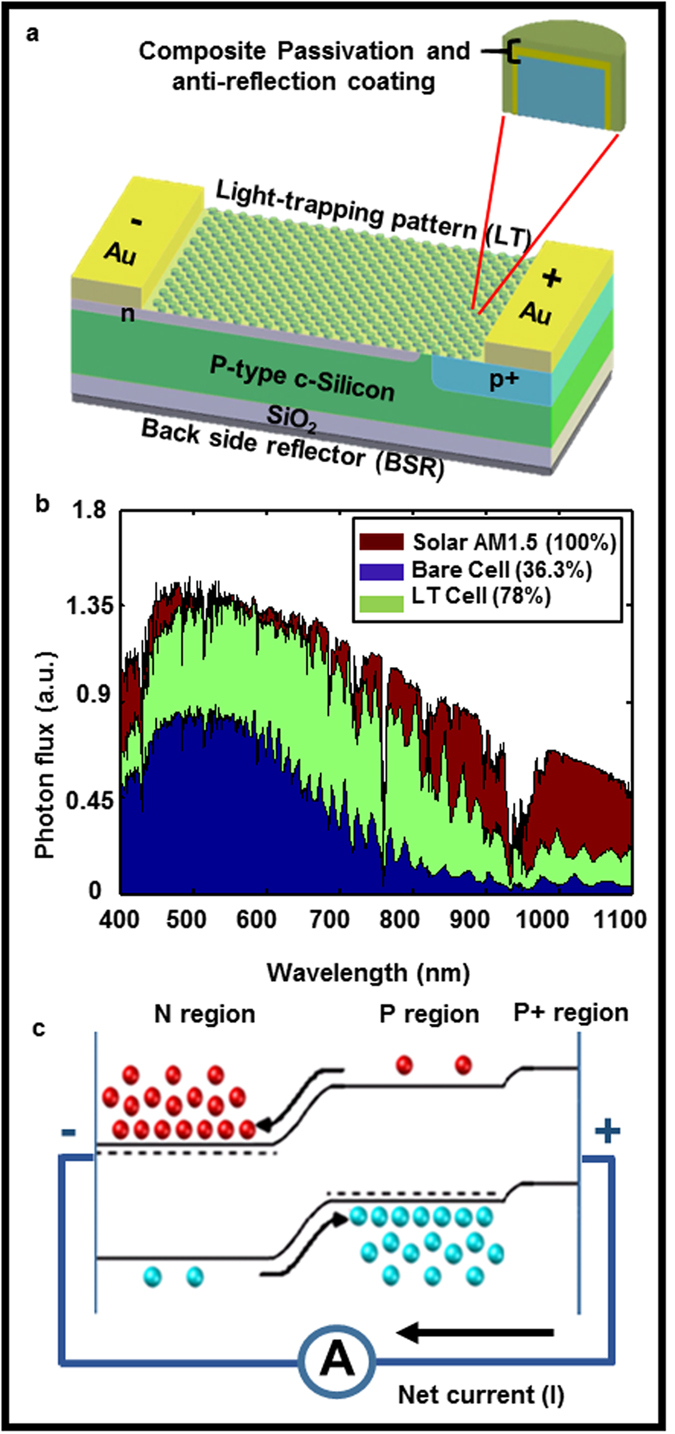
(a) Illustrates the c-Si solar cell architecture which combines the light trapping scheme with the functional cell geometry. (b) The absorbed photo flux as a function of wavelength with reference to AM1.5D solar spectrum for bare and light trapping cell inside a 3 μm thick wafer and (c) the corresponding band diagram under illumination.
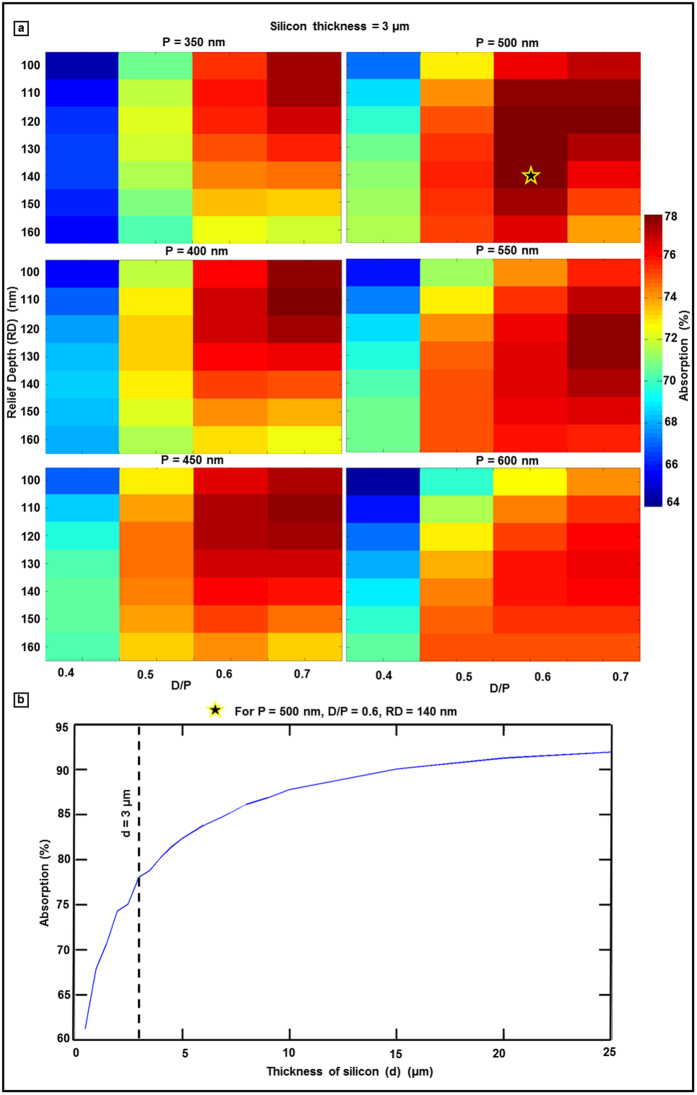
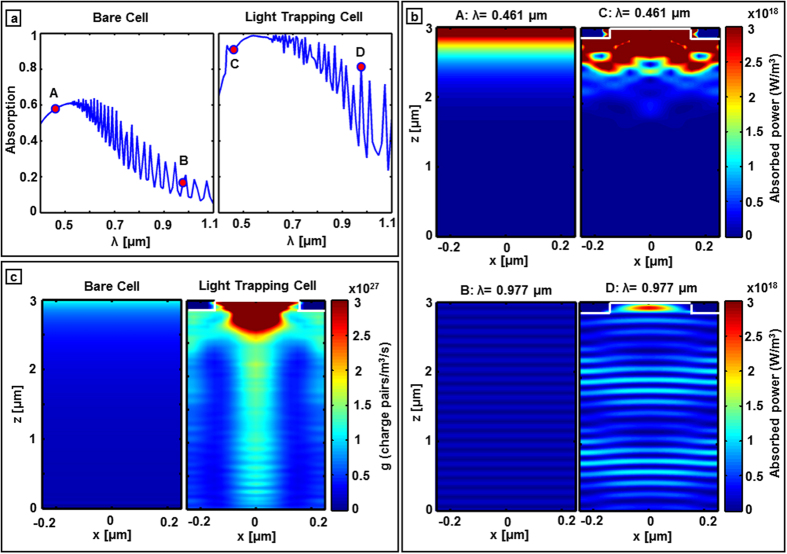
Figure 2(a) shows the 3D FDTD predicted light trapping pattern optimization for a constant silicon thickness (3 μm). The wavelength integrated absorption is maximized as a function of 2D hexagonal lattice period (P), diameter to period ratio (D/P) and relief depth (RD) for a constant ARC layer (SiO2/SiN = 50/35 nm). According to Fig. 2(a), the optimized light trapping pattern which enables the maximum absorption of 78% integrated solar spectrum (400–1100 nm) (marked as star on Fig. 2(a)) defines the posts dimension of period 500 nm, diameter/period 0.6, and relief depth 140 nm. Further based on this optimized pattern, the silicon absorption as a function of silicon thickness is studied and shown in Fig. 2(b). It can be seen that for this light trapping design silicon thickness of >15 μm is needed in order to absorb >90% integrated AM1.5 solar spectrum. Figure 3(a) compares the FDTD predicted absolute absorption of a 3 μm thick bare and a light trapping cell as a function of wavelength. Significant absorption enhancement can be observed in the light trapping cell especially near the band edge where bare silicon absorption is weak. Furthermore, narrow Fabry-Perot cavity resonances are observed in the light trapping cell which correspond to the presence of the 0th and higher order cavity modes of the thin cell. The FDTD predicted 2D absorption profiles (Pabs) of bare and light trapping cells in a strong (λ = 461 nm) and weak (λ = 977 nm) absorption regimes are shown in Fig. 3(b). Absorbed power is obtained by applying equation (1), which is derived from the divergence of the Poynting vector formula as
Figure 2. Light trapping pattern dimension and Si thickness optimization.
(a) FDTD predicted light trapping pattern optimization for a constant silicon thickness (3 μm). The wavelength integrated absorption is maximized as a function of 2D hexagonal lattice period, D/P and relief depth. (b) Silicon absorption as a function of silicon thickness for the optimized light trapping pattern (P = 500 nm, D/P = 0.6, RD = 140 nm with ARC (SiO2/SiN = 50/35 nm)).
Figure 3. Optical characterization of the device.
(a) Compares the FDTD predicted absolute absorption inside 3 μm thick bare and light trapping cells. (b) The power absorbed per unit volume in 3 μm thick bare and light trapping cell at strong (λ = 461 nm) and weak (λ = 977 nm) absorbing regimes. (c) Compares the wavelength integrated charge carrier generation rate (g) over a 2D plane across the center of the hexagonal unit cell.
 |
According to the equation (1), the energy absorption of a monochromatic light is directly proportional to the electric field intensity which mandates field enhancement for higher absorption. As predicted, the band edge photons (λ = 977 nm) are more strongly absorbed in the light trapping cell compared to the bare cell due to tight field confinement and path length enhancement via diffraction/scattering. There is significant enhancement in absorbed power between light trapping and bare cells which can be noticed by comparing Fig. 3(b), top and bottom. This fact is further supported by the wavelength integrated generation rate (g) in Fig. 3(c). The number of electron-hole pairs generated by absorbed photons as a function of position integrated over a specific wavelength range in the device is defined as the wavelength integrated charge carrier generation rate (g). From Fig. 3(c), significantly enhanced charge carrier generation can be observed for the light trapping cell due to the stronger photon absorption substantially deep inside the wafer. Subsequently, the FDTD predicted 3D generation rate data is imported into the numerical electronic modeling (Lumerical DEVICE, Lumerical Inc.) that makes the bridge between electromagnetic absorption and electronic device performance predictions. Since the actual cell is longer than one unit cell due to the lateral p-n junction (Fig. 1(a)), the FDTD predicted one unit cell generation rate, which is calculated with the periodic boundary condition along the x-y directions, is copied along the length of the device to cover the distance between two contacts.
Electronic device modeling
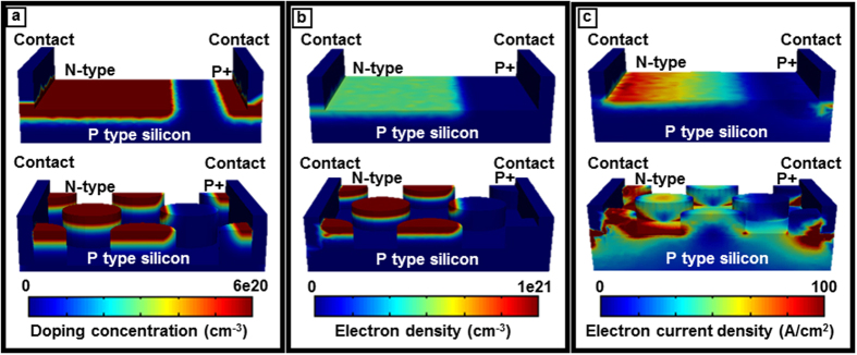
The quasi fermi energy levels, electron-hole densities and recombination losses of the cell were extracted from the electronic simulations in order to understand the fundamental gain and loss mechanisms. For a fair comparison, both bare and light trapping cells are assumed to be perfectly passivated with reasonably low surface recombination velocity (SRV) SRV = 10 m/cm. A low SRV isolates the effects of recombination and electron-hole generation processes. Figure 4(a) shows the chosen doping profile of the 3 μm silicon cell with and without light trapping. The p and n regions are shown as gradient of the doping concentration using two opposite color schemes. Figure 4(b) compares the electron density of a 3 μm bare and light trapping cells. The light trapping cell shows a higher absolute electron (hole) density due to the higher absolute quasi fermi energy levels which, in turn, originates from the higher absorption. The electron density in non-equilibrium conditions (i.e. under illumination as a function of the quasi fermi energy) is given by
Figure 4. Doping and charge carrier generation profile.
(a) The doping profile of the 3 μm thick silicon cell with and without light trapping. The p and n regions are defined which show the gradient of impurities in the device. (b) Compares the electron density of a 3 μm bare cell with light trapping cell. The electron density in n-type region of the light trapping cell is higher than that of the bare cell, and (c) shows the corresponding electron current density. The structure geometries in this figure are not to scale. The color bar upper and lower limits are chosen in order to enhance the contrast.
 |
where  is the effective density of state in the conduction band, εfn, and εc are electron quasi fermi energy and conduction band energy respectively. The carrier density is highly sensitive to any small variation in quasi fermi energy level. As can be seen in Fig. 4(b), the electron density within the n-type region of the light trapping cell is significantly higher than that of the bare cell. The n and p quasi fermi energy difference (εfn − εfp) is a measure of the deviation from equilibrium. Under non-equilibrium conditions, i.e. under illumination, the current density can be written as
 |
where μn is the electron mobility. The electron density in the non-equilibrium condition is n = n0 + Δn where n0 is the donor impurity concentration (at equilibrium) and Δn is the excess minority carrier concentration that is generated under illumination. The higher value of charge density, in conjunction with higher quasi fermi energy, leads to a greater electron current density. Figure 4(c) illustrates the electron current density enhancement in light trapping cell with respect to the bare cell. Current density that is proportional to the gradient of the quasi fermi level, shows the flow of photo generated carriers towards ohmic contacts and through the external circuit. The concentration of holes and corresponding hole current density can be explained in a similar fashion. For fair comparison, both electron density and current density (Fig. 4(b,c)) are integrated over the corresponding predicted I-V curve shown in the following.
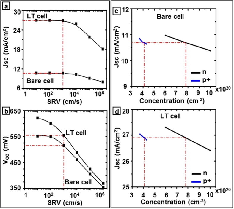
Apart from the light absorption enhancement in the light trapping cell, which leads to higher internal current density as demonstrated above, it is also important to investigate the mechanisms of loss in order to improve charge collection and overall cell efficiency. The surface recombination velocity (SRV), which is one of the main sources of voltage loss and low short circuit current, defines the carrier recombination rate at the silicon interfaces due to the silicon dangling bonds. Figure 5(a) shows the predicted variation in Jsc as a function of SRV for bare and light trapping cells. Although, a lower SRV (1–100 cm/s)30,31,32,33 produces higher Jsc, achieving such low SRV on a patterned surfaces of a light trapping cell requires excellent surface passivation. The impact of bulk and surface recombination on the cell performance can be described by the effective lifetime, given by30,34,35
Figure 5. Effect of surface recombination and doping concentration.
(a,b) The predicted short circuit current density (Jsc) and open circuit voltage (Voc) as a function of surface recombination velocity in the top and bottom graphs respectively, and (c,d) show the predicted short circuit current density as a function of doping concentration for both bare and light trapping cells.
 |
where d is the cell thickness. According to the equation (4), in lower cell thicknesses, SRV becomes more significant than the bulk lifetime. Thus a good multi-functional passivation layer on the patterned top surface which also functions as an anti-reflection coating makes a significant difference in device performance due to both photon absorption enhancement and carrier lifetime improvement. The SRV further influences the open circuit voltage which is defined in equation (5) for a solar cell made on a p-type wafer as36,37,38
 |
where Jph is photocurrent density, NA is the acceptor concentration, ∆n and ∆p are the electron and hole excess minority carrier concentration respectively which are equivalent under the illumination in solar cells, and ni is the intrinsic carrier concentration. Since SRV is inversely related to the lifetime, τeff (Equation (4)), it reduces the open circuit voltage as can be observed in Fig. 5(b), and ultimately the energy conversion efficiency of the cell. Both the current density and the voltage (Fig. 5(a,b) of the light trapping cell decreases significantly compared to that of the bare cell as SRV increases. This sharp fall can be explained by higher surface recombination due to the surface texturing in light trapping cells. Figure 5(c,d) shows the short circuit current density vs doping concentrations for boron and phosphorus regions in bare and light trapping cells respectively for the surface recombination velocity of 1000 cm/s. A SRV of 1000 cm/s is chosen for the doping concentration studies since lower SRVs can only be obtained by thermal silicon oxide growth which is not applicable in this case due to polymeric substrates of fabricated microbar cells29,39. A significant enhancement in Jsc can be observed in the light trapping cell compared to the bare cell. The phosphorus and boron doping concentration studied regime is 6e + 20–1e + 21 cm−3 and 3.7e + 20–4.3e + 20 cm3, respectively. These variation ranges are based upon the pre-deposition furnace temperature of 900 °C–1050 °C in which the cells are exposed to the infinite constant sources40. Since our studied cell is ultrathin, 3 μm, compared to conventional silicon solar cell thickness (150–180 μm) the drive-in diffusion process that is occurred at higher temperature (T > 1000 °C) in the absence of the dopant source in order to increase the junction depth is not considered in this study. These results imply that lower doping concentration leads to higher current densities, at the studied doping concentration regime41 which also can be shown theoretically by:
 |
where J0 is the dark current which flows through the solar cell when a bias is applied in the dark and in low level injection is given by:
 |
Dn, Dp are the electron and hole diffusion coefficients, τn, τp are the lifetime of electron and hole, respectively. Comparing Eq. (6) and Eq. (7) we can conclude that a lower doping concentration (NA, ND) leads to higher J0 and consequently higher Jsc as observed in the numerical simulation in Fig. 5(c,d).
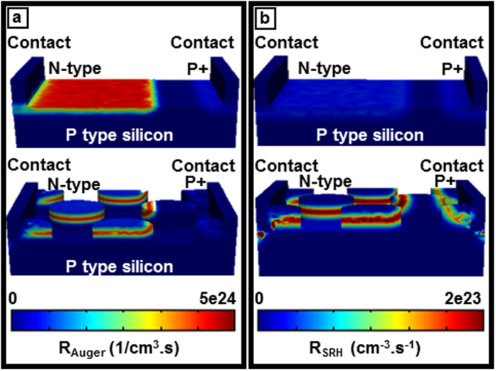
Deep level or Shockley-Read-Hall (SRH) and Auger recombination are the other two carrier loss mechanisms which severely affect solar cell performance. The more heavily doped material leads to higher auger recombination and the material with more defect states has higher Shockley-Read-Hall recombination. These recombination mechanisms are defined as42:
 |
where  ,
,  , τn0, τp0 are SRH electron and hole lifetime,
 is trapping energy level, and:
 |
where Cp0, Cn0 are auger coefficients which have inverse quadratic dependence upon carrier concentration (unit cm6/s). From Fig. 6(a,b) it can be seen that the light trapping cell has a higher Auger and Shockley-Read-Hall recombination rate within the posts due to the generation of higher excessive minority carriers and higher defect density, respectively. Both recombination rates are integrated over the respective I-V curve (Fig. 7(b)) of bare and light trapping cells in order to demonstrate the overall response. The light trapping nano-patterning introduces more localized doping distribution and more defects to the silicon cell which leads to higher auger and SRH recombination. However, enhanced absorption and carrier generation in light trapping cells compensates these recombination losses and gives a higher overall cell efficiency. Further, this work shows that the device performance can be enhanced by minimizing recombination losses via optimum doping profile and surface passivation.
Figure 6. Recombination losses.
(a,b) Compares the Auger and Shockley-Read-Hall recombination in bare and light trapping cells, respectively. Light trapping cell possesses higher recombination due to higher localized doping concentration and defect density. The cell geometry is not to scale.
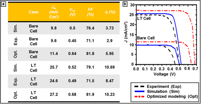
Figure 7. Comparison of the fabricated and predicted device performance.
(a) Short circuit current (Jsc), open circuit voltage (Voc), fill factor (FF), and efficiency (η) of fabricated, simulated and optimized 3 μm bare and light trapping solar cells and corresponding I-V curves are shown in (b).
Device optimization and simulation parameters
The device simulation parameters are presented in the Table (1) for two conditions: specific to the fabricated and the optimum cells. The values for the predicted cell were chosen to be either equivalent or close to the experimental conditions. There are some discrepancies between predicted and measured cell performances primarily due to the mismatch between estimated device parameters like carrier life time, SRV, sidewall ARC thickness on the patterned surface, doping profile and actual experimental cell. The detailed light trapping pattern design and fabrication is reported in our previous publications29. Soft nanoimprint lithography (NIL) and reactive ion etching defines hexagonal cylindrical silicon posts of period 500 nm, diameter 300 nm and relief depth 140 nm as light trapping pattern which are optimized with FDTD simulation as shown in Fig. 2(a). A layer of PECVD SiNx (20–50 nm) and SiO2 (~50–80 nm) deposition the device serves as anti-reflection coating (ARC) and passivation layer. Different techniques of minimizing the reflection losses such as single dielectric layer, gradient refractive index layers, and nanostructured surfaces are commonly used43,44,45. A 200 nm thick gold layer serves as backside reflector (BSR). The top diffractive optics pattern functions as grating coupler to couple incoming solar radiation as diffracted/scattered modes thus enhancing effective path length. The functional cell fabrication is completed with the doping of boron and phosphorus through patterned hard masks to define the P-N junctions followed by metal contact formation as schematically shown in Fig. 1(a). These parameters are fixed for both bare and light trapping cells in order to compare and focus on the impact of light trapping on the device performance. The predicted results and experimentally measured data28 of a 3 μm thick microbar silicon solar cell are tabulated and plotted side by side for the comparison in Fig. 7(a,b), respectively. As shown in the table Fig. 7(a), the predicted Jsc and Voc closely match experimental measurements for both bare and light trapping cells. The energy conversion efficiency enhancement prediction of 186% closely matches the experimentally measured enhancement of 192% of the light trapping cell with respect to the bare cell measurement. The main difference between the predicted and the fabricated cell is the Voc that is most likely caused by non-uniform back surface field (BSF) of the fabricated cell. The optimized light trapping and bare cells show 105% and 80% percentages of improvements with respect to corresponding experimentally fabricated cells, respectively. The optimum cell design considered an ideal carrier life time and SRVs as tabulated in Table (1) in order to establish a maximum possible cell performance. For the optimized cell we used a SRV of 10 cm/s and bulk life time of 1 ms as tabulated in Table 1. Such range of low SRV and long carrier life time is indeed achievable via high quality surface passivation as demonstrated in refs 19,46,47. The 3D device simulation of charge carrier generation/recombination in bare and light trapping cells in thin-film geometry in this study distinctively showed the inter-relation between various processes. The study also defined parameter space (doping profile, junction depth, SRV etc.) for optimum performance of a 3 μm thick light trapping solar cell. The future work will focus on bridging the gap between the present and the optimal cell performances following this unified electromagnetic-electronic design approach presented above.
Table 1. The electrical simulation parameters of the fabricated (Sim.) and optimized (Opt.) bare and light trapping cells.
| Wafer conc. (1/cm3) | p + surface conc. (1/cm3) | p + junc. width (nm) | n surface conc. (1/cm3) | n Junc. width (nm) | Electron Carrier lifetime (ms) | Hole Carrier lifetime (ms) | SRV (cm/s) | BSF conc. (1/cm3) | BSF junc. width (nm) | |
|---|---|---|---|---|---|---|---|---|---|---|
| Opt. | 1015 | 3.7E + 20 | 154 | 6E + 20 | 158 | 1 | 1 | 10 | 4.1E + 20 | 186 |
| Sim. | 1015 | 4.1E + 20 | 416 | 7.8E + 20 | 140 | 10−3 | 10−4 | 104 | 4.1E + 20 | 186 |
We theoretically demonstrated an optimized 3 μm thick light trapping cell in order to show what can be achieved in terms of device performance following this unified design approach. The light trapping scheme showed significant enhancement in band edge photon absorption resulting in higher charge carrier generation rate. Although surface nano-patterning causes more recombination, its impact on the overall cell efficiency enhancement is significant due to the stronger light absorption and higher generation rate which outweighs recombination losses. Such a unified electromagnetic-electronic design approach will help design better solar cell architecture with higher energy conversion efficiency.
Additional Information
How to cite this article: Boroumand, J. et al. Unified Electromagnetic-Electronic Design of Light Trapping Silicon Solar Cells. Sci. Rep. 6, 31013; doi: 10.1038/srep31013 (2016).
Acknowledgments
This work at University of Central Florida was supported by the National Science Foundation (grant no. #CMMI-1450806). J. Boroumand would like to thank K.J. Yu and J. Rogers from University of Illinois at Urbana-Champaign Urbana, for the valuable help.
Footnotes
Author Contributions D.C. conceived the idea. J.B. designed and performed the experiments. J.B. and S.D. analyzed and simulated the data. A.V.-G. and D.F. provided technical guidance. J.B. and D.C. co-wrote the paper.
References
- Wolden C. A. et al. Photovoltaic manufacturing: Present status, future prospects, and research needs. J Vac Sci Technol A 29, 030801, doi: 10.1116/1.3569757 (2011). [DOI] [Google Scholar]
- Frühauf J., Gärtner E. & Krönert S. Shape and Functional Elements of the Bulk Silicon Microtechnique. 1 edn, (Springer-Verlag Berlin Heidelberg, 2005). [Google Scholar]
- Green M. A. Silicon Solar Cells Advanced Principles (1995).
- Hegedus S. & Luque A. In Handbook of Photovoltaic Science and Engineering 1–38 (John Wiley & Sons, Ltd., 2011). [Google Scholar]
- Bagnall D. M. & Boreland M. Photovoltaic technologies. Energy Policy 36, 4390–4396, doi: 10.1016/j.enpol.2008.09.070 (2008). [DOI] [Google Scholar]
- Saga T. Advances in crystalline silicon solar cell technology for industrial mass production. NPG Asia Materials 2, 96–102, doi: 10.1038/asiamat.2010.82 (2010). [DOI] [Google Scholar]
- Petti C., Newman B., Brainard R. & Li J. Optimal thickness for crystalline silicon solar cells 1–15 (2011). [Google Scholar]
- Tool C. J. J., Burgers A. R., Manshanden P., Weeber A. W. & van Straaten B. H. M. Influence of wafer thickness on the performance of multicrystalline Si solar cells: an experimental study. Prog Photovoltaics 10, 279–291, doi: 10.1002/pip.421 (2002). [DOI] [Google Scholar]
- Wolf M. Updating the Limit Efficiency of Silicon Solar-Cells. Ieee Transactions on Electron Devices 27, 751–760, doi: 10.1109/T-Ed.1980.19932 (1980). [DOI] [Google Scholar]
- Pillai S., Catchpole K. R., Trupke T. & Green M. A. Surface plasmon enhanced silicon solar cells. Journal of Applied Physics 101, 093105, doi: 10.1063/1.2734885 (2007). [DOI] [Google Scholar]
- Guo X. et al. Two- and three-dimensional folding of thin film single-crystalline silicon for photovoltaic power applications. Proceedings of the National Academy of Sciences of the United States of America 106, 20149–20154, doi: 10.1073/pnas.0907390106 (2009). [DOI] [PMC free article] [PubMed] [Google Scholar]
- Yao Y., Brueckner E., Li L. F. & Nuzzo R. Fabrication and assembly of ultrathin high-efficiency silicon solar microcells integrating electrical passivation and anti-reflection coatings. Energy & Environmental Science 6, 3071–3079, doi: 10.1039/c3ee42230e (2013). [DOI] [Google Scholar]
- Mavrokefalos A., Han S. E., Yerci S., Branham M. S. & Chen G. Efficient light trapping in inverted nanopyramid thin crystalline silicon membranes for solar cell applications. Nano letters 12, 2792–2796, doi: 10.1021/nl2045777 (2012). [DOI] [PubMed] [Google Scholar]
- Wang K. X., Yu Z., Liu V., Cui Y. & Fan S. Absorption enhancement in ultrathin crystalline silicon solar cells with antireflection and light-trapping nanocone gratings. Nano letters 12, 1616–1619, doi: 10.1021/nl204550q (2012). [DOI] [PubMed] [Google Scholar]
- Corcoran C. J. et al. Mechanisms of enhanced optical absorption for ultrathin silicon solar microcells with an integrated nanostructured backside reflector. ACS applied materials & interfaces 5, 4239–4246, doi: 10.1021/am400408g (2013). [DOI] [PubMed] [Google Scholar]
- Wang Z. Y. et al. Broadband optical absorption by tunable Mie resonances in silicon nanocone arrays. Scientific reports 5, 7810, doi: 10.1038/srep07810 (2015). [DOI] [PMC free article] [PubMed] [Google Scholar]
- Chong T. K., Wilson J., Mokkapati S. & Catchpole K. R. Optimal wavelength scale diffraction gratings for light trapping in solar cells. Journal of Optics 14, 024012, doi: 10.1088/2040-8978/14/2/024012 (2012). [DOI] [Google Scholar]
- Wang S. et al. Large-area free-standing ultrathin single-crystal silicon as processable materials. Nano letters 13, 4393–4398, doi: 10.1021/nl402230v (2013). [DOI] [PubMed] [Google Scholar]
- Branham M. S. et al. 15.7% Efficient 10-mum-thick crystalline silicon solar cells using periodic nanostructures. Advanced materials 27, 2182–2188, doi: 10.1002/adma.201405511 (2015). [DOI] [PubMed] [Google Scholar]
- Callahan D. M., Munday J. N. & Atwater H. A. Solar Cell light trapping beyond the ray optic limit. Nano letters 12, 214–218, doi: 10.1021/nl203351k (2012). [DOI] [PubMed] [Google Scholar]
- Kelzenberg M. D. et al. Enhanced absorption and carrier collection in Si wire arrays for photovoltaic applications. Nature materials 9, 239–244, doi: 10.1038/nmat2635 (2010). [DOI] [PubMed] [Google Scholar]
- Fan Z. et al. Ordered arrays of dual-diameter nanopillars for maximized optical absorption. Nano letters 10, 3823–3827, doi: 10.1021/nl1010788 (2010). [DOI] [PubMed] [Google Scholar]
- Brongersma M. L., Cui Y. & Fan S. H. Light management for photovoltaics using high-index nanostructures. Nature materials 13, 451–460, doi: 10.1038/Nmat3921 (2014). [DOI] [PubMed] [Google Scholar]
- Ko M. D., Rim T., Kim K., Meyyappan M. & Baek C. K. High efficiency silicon solar cell based on asymmetric nanowire. Scientific reports 5, 11646, doi: 10.1038/srep11646 (2015). [DOI] [PMC free article] [PubMed] [Google Scholar]
- Dewan R., Jovanov V., Hamraz S. & Knipp D. Analyzing periodic and random textured silicon thin film solar cells by Rigorous Coupled Wave Analysis. Scientific reports 4, 6029, doi: 10.1038/srep06029 (2014). [DOI] [PMC free article] [PubMed] [Google Scholar]
- Li G., Li H., Ho J. Y., Wong M. & Kwok H. S. Nanopyramid structure for ultrathin c-Si tandem solar cells. Nano letters 14, 2563–2568, doi: 10.1021/nl500366c (2014). [DOI] [PubMed] [Google Scholar]
- Shir D., Yoon J., Chanda D., Ryu J. H. & Rogers J. A. Performance of Ultrathin Silicon Solar Microcells with Nanostructures of Relief Formed by Soft Imprint Lithography for Broad Band Absorption Enhancement. Nano Lett. 10, 3041–3046 (2010). [DOI] [PubMed] [Google Scholar]
- Ki Jun Yu et al. Light Trapping in Ultra-thin Monocrystalline Silicon Solar Cells. Advanced Energy Materials 3, 1401–1406 (2013). [Google Scholar]
- Yu K. J. et al. Light Trapping in Ultrathin Monocrystalline Silicon Solar Cells. Advanced Energy Materials 3, 1401–1406, doi: 10.1002/aenm.201300542 (2013). [DOI] [Google Scholar]
- Chen Z., Pang S. K., Yasutake K. & Rohatgi A. Plasma-enhanced chemical-vapor-deposited oxide for low surface recombination velocity and high effective lifetime in silicon. Journal of Applied Physics 74, 2856, doi: 10.1063/1.354638 (1993). [DOI] [Google Scholar]
- Bikbajevas V., Grivickas V., Linnros J. & Tellefsen J. A. Injection-level dependent surface recombination velocities at the Si-SiO2 interface. Physica Scripta T79, 322–326, doi: 10.1238/Physica.Topical.079a00322 (1999). [DOI] [Google Scholar]
- Grant N. & McIntosh K. In Conference Proceedings Solar (Australian Solar Energy Society, 2010).
- Aberle A. G., Glunz S. & Warta W. Impact of Illumination Level and Oxide Parameters on Shockley-Read-Hall Recombination at the Si-Sio2 Interface. Journal of Applied Physics 71, 4422–4431, doi: 10.1063/1.350782 (1992). [DOI] [Google Scholar]
- Schultz O., Glunz S. W. & Willeke G. P. SHORT COMMUNICATION: ACCELERATED PUBLICATION: Multicrystalline silicon solar cells exceeding 20% efficiency. Progress in Photovoltaics: Research and Applications 12, 553–558, doi: 10.1002/pip.583 (2004). [DOI] [Google Scholar]
- Cuevas A. & Macdonald D. Measuring and interpreting the lifetime of silicon wafers. Solar Energy 76, 255–262, doi: 10.1016/j.solener.2003.07.033 (2004). [DOI] [Google Scholar]
- Jensen N. et al. Recombination mechanisms in amorphous silicon/crystalline silicon heterojunction solar cells. Journal of Applied Physics 87, 2639, doi: 10.1063/1.372230 (2000). [DOI] [Google Scholar]
- Pisarkiewicz T. Photodecay method in investigation of materials and photovoltaic structures. Opto-Electron Rev 12, 33–40 (2004). [Google Scholar]
- Sinton R. A. & Cuevas A. Contactless determination of current-voltage characteristics and minority-carrier lifetimes in semiconductors from quasi-steady-state photoconductance data. Applied Physics Letters 69, 2510–2512, doi: 10.1063/1.117723 (1996). [DOI] [Google Scholar]
- Shir D., Yoon J., Chanda D., Ryu J. H. & Rogers J. A. Performance of ultrathin silicon solar microcells with nanostructures of relief formed by soft imprint lithography for broad band absorption enhancement. Nano letters 10, 3041–3046, doi: 10.1021/nl101510q (2010). [DOI] [PubMed] [Google Scholar]
- Anner G. E. Planar processing primer. (Van Nostrand Reinhold, 1990). [Google Scholar]
- STEM N. & CID M. Studies of phosphorus Gaussian profile emitter silicon solar cells. Materials Research 4, 143–148 (2001). [Google Scholar]
- Luque A. & Hegedus S. Handbook of photovoltaics science and engineering. 2 edn, (John Wiley & Sons, 2011). [Google Scholar]
- Raut H. K., Ganesh V. A., Nair A. S. & Ramakrishna S. Anti-reflective coatings: A critical, in-depth review. Energy & Environmental Science 4, 3779–3804, doi: 10.1039/c1ee01297e (2011). [DOI] [Google Scholar]
- Baryshnikova K. V., Petrov M. I., Babicheva V. E. & Belov P. A. Plasmonic and silicon spherical nanoparticle antireflective coatings. Scientific reports 6, 22136, doi: 10.1038/srep22136 (2016). [DOI] [PMC free article] [PubMed] [Google Scholar]
- Shi D., Zeng Y. & Shen W. Perovskite/c-Si tandem solar cell with inverted nanopyramids: realizing high efficiency by controllable light trapping. Scientific reports 5, 16504, doi: 10.1038/srep16504 (2015). [DOI] [PMC free article] [PubMed] [Google Scholar]
- Jeong S., McGehee M. D. & Cui Y. All-back-contact ultra-thin silicon nanocone solar cells with 13.7% power conversion efficiency. Nature communications 4, 2950, doi: 10.1038/ncomms3950 (2013). [DOI] [PubMed] [Google Scholar]
- Yoon J. et al. Ultrathin silicon solar microcells for semitransparent, mechanically flexible and microconcentrator module designs. Nature materials 7, 907–915, doi: 10.1038/nmat2287 (2008). [DOI] [PubMed] [Google Scholar]


