Significance
The performances of devices based on transition metal dichalcogenides (TMDs) are far from their intrinsic limits, presumably due to various disorders in these 2D crystals. To date, little is known about the magnitude and characteristic length scale of electrical inhomogeneity induced by the disorders in TMDs. In this paper, strong mesoscopic (submicrometer) electrical inhomogeneity in MoS2 flakes, which reveals the potential fluctuations, was observed by a unique technique termed microwave impedance microscopy. The local conductance of edge states and its contribution to the transport were also resolved and analyzed experimentally for the first time, to our knowledge. The results provide a comprehensive understanding of the potential landscape in TMDs, which is very important for the improvement of device performance.
Keywords: MoS2, microwave impedance microscopy, edge states, electrical inhomogeneity, metal-insulator transition
Abstract
The understanding of various types of disorders in atomically thin transition metal dichalcogenides (TMDs), including dangling bonds at the edges, chalcogen deficiencies in the bulk, and charges in the substrate, is of fundamental importance for TMD applications in electronics and photonics. Because of the imperfections, electrons moving on these 2D crystals experience a spatially nonuniform Coulomb environment, whose effect on the charge transport has not been microscopically studied. Here, we report the mesoscopic conductance mapping in monolayer and few-layer MoS2 field-effect transistors by microwave impedance microscopy (MIM). The spatial evolution of the insulator-to-metal transition is clearly resolved. Interestingly, as the transistors are gradually turned on, electrical conduction emerges initially at the edges before appearing in the bulk of MoS2 flakes, which can be explained by our first-principles calculations. The results unambiguously confirm that the contribution of edge states to the channel conductance is significant under the threshold voltage but negligible once the bulk of the TMD device becomes conductive. Strong conductance inhomogeneity, which is associated with the fluctuations of disorder potential in the 2D sheets, is also observed in the MIM images, providing a guideline for future improvement of the device performance.
Electrostatic gating in the field-effect transistor (FET) configuration has played an essential role in the blooming field of semiconducting transition metal dichalcogenides (TMDs) such as MoS2 and WSe2 (1). The electrical control of carrier densities in these naturally formed 2D sheets is crucial for the realization of many intriguing phenomena, such as the metal−insulator transition (2–6), novel spin and valley physics (7–12), and superconducting phases (13–15). In addition, the carrier modulation provides an ideal tuning parameter to study the screening effect, which is particularly important for charge transport in 2D materials that are highly susceptible to local variations of the disorder potential (2–5, 16, 17). As a result, a complete understanding of the electronic properties of TMD FETs at all length scales, i.e., from local defects in the atomic scale, to electronic inhomogeneity in the mesoscale, to device performance in the macroscale, is imperative for both fundamental research on and practical applications of these fascinating materials.
Transport and most optical measurements on TMD FETs are inherently macroscopic in nature, in which the sample response is averaged over large areas. TMD films in actual devices, however, are far from electronically uniform. Due to the relatively large amount of intrinsic defects and the inevitable charged states in the substrates, mesoscopic electrical inhomogeneity is not uncommon in TMDs, leading to hopping transport and percolation transition in the devices (6, 16–19). Little is known, however, about the magnitude and characteristic length scale of such conductance fluctuations. For layered van der Waals materials, another unique feature occurs at the sample edges, where the broken crystalline symmetry and the presence of dangling bonds introduce additional electronic states to the bulk band structure. To date, edge states in TMDs are theoretically studied by first-principles calculations (20–22) and experimentally probed by scanning tunneling microscopy (STM) and spectroscopy (20, 23), whereas their contribution to the overall charge transport has not been fully addressed. Spatially resolved conductance maps are therefore highly desirable for the understanding of electrical inhomogeneity and edge channels in TMD FETs.
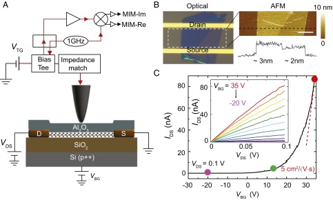
In this paper, we report the microwave impedance microscopy (MIM) (24, 25) study on the nanoscale conductance distribution during the normal operation of MoS2 FETs. The experimental setup for our simultaneous transport and MIM measurements is schematically illustrated in Fig. 1A. The MoS2 FETs and the MIM tip are mounted on the sample stage and the z scanner of a commercial atomic force microscope (AFM), respectively. During the contact-mode AFM scans, a low-power (∼10 μW) 1-GHz microwave signal is delivered to the shielded cantilever tip (26) through the impedance match section. A dc bias can also be coupled to the tip using a bias tee. The reflected signal is then amplified and demodulated to form the MIM-Im and MIM-Re signals, which are proportional to the imaginary and real parts, respectively, of the small changes of tip−sample admittance in the measurement. Using the standard finite element analysis (FEA) modeling (24), the local sample conductivity can be mapped out with a spatial resolution determined by the tip diameter (on the order of 100 nm) rather than the free-space wavelength (λ = 30 cm) of the 1-GHz microwave. The conductance fluctuation in this mesoscopic regime is particularly important for macroscopic device performance.
Fig. 1.
Experimental setup and device characterization. (A) Schematic diagram of the device and the MIM setup. The 1-GHz microwave signal is guided to the tip through an impedance match section, and the reflected signal is detected by the MIM electronics. The carrier density can be either globally tuned by the back-gate voltage VBG or locally modulated by the dc bias on the tip VTG. (B) Optical and the zoom-in AFM images of an exfoliated MoS2 FET device. (Inset) A line profile across the surface. (Scale bar, 5 μm.) (C) Transfer characteristics of the device at VDS = 0.1 V. The dashed line is a linear fit to the curve for VBG > 30 V, from which the field-effect mobility μFE ∼ 5 cm2/(V⋅s) can be deduced. The solid circles (purple, green, and red) match the color coding in Fig. 5. (Inset) The output characteristics from VBG = 35 V to −20 V with 5-V steps.
Results and Discussion
The starting materials of our FETs are few-layer exfoliated and monolayer (ML) chemical vapor deposited (CVD) MoS2 flakes. The samples were transferred to or directly grown on SiO2 (285 nm)/Si substrates, after which the source and drain contacts (20 nm Ag/30 nm Au) were formed via conventional electron beam (e beam) lithography and deposition (27, 28). To avoid direct contact between the metallic tip and the 2D sheets, which would strongly perturb the semiconducting MoS2, we covered the device by the e-beam deposition of a thin (15 nm) layer of Al2O3. As a result, the carrier density in MoS2 can be either globally modulated by the heavily doped Si back gate or locally tuned by the tip as a scanning top gate. Thanks to the capacitive tip−sample interaction, the MIM is capable of preforming subsurface electrical imaging (29–32) on the buried MoS2 nanosheets.
Multiple exfoliated and CVD MoS2 devices were investigated in this work, all of which exhibited similar behaviors. Fig. 1B shows the optical and the close-up AFM images of a typical FET fabricated on an exfoliated flake. The sample consists of two distinct regions with thicknesses of 2.1 nm and 2.8 nm, corresponding to three and four MLs, respectively, of MoS2. Excluding several wrinkles from the exfoliation, the surface roughness of the sample is about 0.4 nm, presumably due to the fabrication process and Al2O3 deposition. The linear output characteristic IDS−VDS curves in Fig. 1C, Inset at different back-gate voltages (VBG) are indicative of the good Ohmic contacts between Ag and MoS2 (27). From the n-type transfer characteristics in Fig. 1C, the field effect mobility can be extracted by using the expression , where Cox is the parallel-plate capacitance of the SiO2 layer, and L and W are the channel length and width, respectively. Note that, although the room temperature mobility is comparable to that of most back-gated devices reported in the literature (3, 5, 6, 16, 17), it is much lower than the theoretical phonon-limited value (33), suggesting the presence of considerable disorder in this device, which will be explored by the MIM study below.
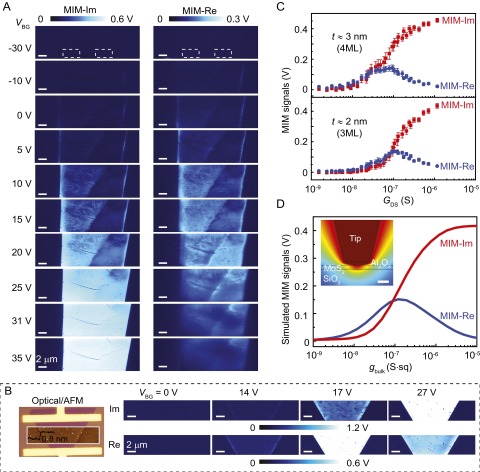
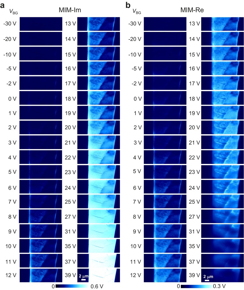
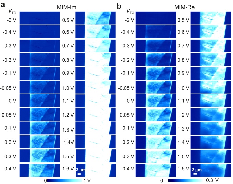
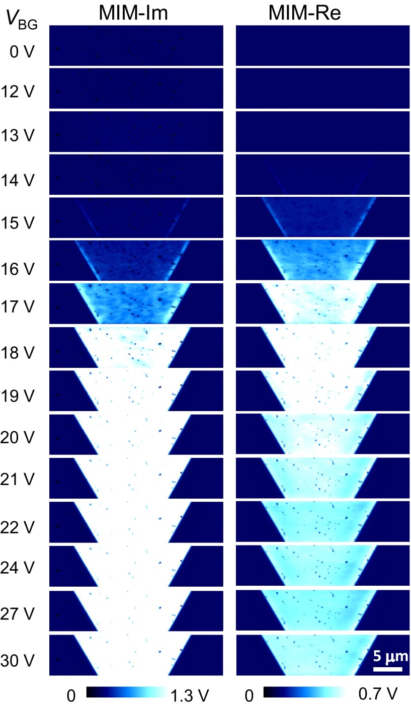
Fig. 2A displays selected MIM images within the channel region of the device in Fig. 1B as a function of VBG. The complete set of data and a video clip showing the gate dependence can be found in Fig. S1 and Movie S1, respectively. The evolution of local conductance maps vividly demonstrates the insulator-to-metal transition induced by the electrostatic field effect. When the flake is in the insulating limit at VBG = −30 V, there is virtually no electrical contrast between MoS2 and the substrate. As VBG gradually goes up to 0 V, the contrast first emerges at the edges of the flake and then in the interior of the sample. Note that the MIM-Im signals are always higher on the four-ML region, with slightly smaller band gap (34) and higher mobility (35) than the three-ML part. For increasing VBG toward 20 V, strong inhomogeneity is observed in both MIM output channels. At the same time, the MIM signals at the edges gradually merge into the bulk and become indistinguishable with the rest of the flake for VBG > 20 V. For even higher back-gate voltages, the sample appears uniformly bright in MIM-Im and dim in MIM-Re. During the entire process, the MIM-Im signals on the MoS2 flake rise monotonically as increasing VBG, whereas the MIM-Re signals reach a peak at VBG ∼20 V and diminish afterward. Similar MIM data are observed by gradually ramping up the dc tip bias VTG during the scans, as shown in Fig. S2. The local gating, on the other hand, results in a complex in-plane potential gradient away from the tip (36) and therefore will not be analyzed in detail here. We emphasize that the same trend of MIM response has been seen in all six MoS2 FETs in this study. Fig. 2B shows the optical, AFM, and MIM images of a CVD-grown ML MoS2 device (complete set of data included in Fig. S3), with the overall behavior similar to that in Fig. 2A. In the following, we will focus on the exfoliated sample in Fig. 1 for quantitative analysis of the MIM data.
Fig. 2.
Overall MIM response during the insulator-to-metal transition. (A) MIM-Im and MIM-Re images in the channel region (zoom-in image in Fig. 1B) of the device at selected back-gate voltages. (B) Optical, AFM (Inset), and MIM images of another FET device fabricated on a CVD-grown ML MoS2 flake (see Fig. S3 for details). (A and B scale bars, 2 μm.) (C) Average MIM signals inside the white dashed boxes in A as a function of the source−drain conductance GDS. (D) Simulated MIM signals as a function of the bulk sheet conductance gbulk, showing very good agreement with the measured data in C. (Inset) The modeling geometry and the quasi-static potential distribution when the MoS2 layer is insulating. (Scale bar, 50 nm.)
Fig. S1.
Complete set of MIM data at different back-gate voltages. (A) MIM-Im and (B) MIM-Re images of the device channel. A video showing the evolution is provided in Movie S1.
Fig. S2.
MIM images at different top-gate voltages. (A) MIM-Im and (B) MIM-Re images on the same area of the device as in Fig. 2A. The features are similar to that of the back-gated data. As VTG increases from −2 V to 1.6 V, MIM-Im signals increase monotonically, whereas MIM-Re signals reach a peak around VTG = 1.5 V and then diminish. The bright edges are also observed at low VTG before the bulk becomes conductive. Significant electrical inhomogeneity is visualized, as well, before the saturation of MIM signals.
Fig. S3.
MIM-Im (Left) and MIM-Re (Right) images of a device fabricated on a CVD-grown MoS2 flake at different back-gate voltages. The overall evolution of MIM signals as a function of VBG, the emergence of edge states (e.g., at VBG = 14 V), and the conductance inhomogeneity (e.g., at VBG = 17 V) are again observed in this sample. Note that different color scales compared with the data of exfoliated sample are adopted here for better visualization, because a different MIM tip was used and the MIM contrasts were different. For different tips, a calibration on standard sample and Im/Re are used for quantitative analysis (46).
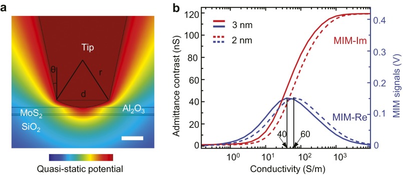
The average MIM-Im/Re signals within two 4 μm × 2 μm areas (white dashed boxes in Fig. 2A) on the four-ML and three-ML segments are shown in Fig. 2C, where the x axis is converted from VBG to the two-terminal source−drain conductance (GDS) by using the transfer curve in Fig. 1C. To quantitatively interpret the MIM signals as local conductance, we have calculated the MIM response curves as a function of the bulk MoS2 sheet conductance gbulk using FEA (24). Details of the FEA modeling and justification of the simulation parameters are included in Fig. S4. As shown in Fig. 2D, the simulated MIM-Im signal, which is proportional to the tip−sample capacitance, increases monotonically as increasing gbulk and saturates at both the insulating (gbulk < 10−9 Siemens·sq or S⋅sq) and conducting (gbulk > 10−5 S⋅sq) limits. The MIM-Re signal, on the other hand, represents the effective loss in the tip−sample interaction and peaks at an intermediate gbulk of ∼10−7 S⋅sq. Note that GDS ≈ gbulk⋅W/L if the source/drain contact resistance is relatively small compared with the channel resistance. An excellent agreement between the experimental data and our modeling result can be obtained by comparing the averaged MIM signals in Fig. 2C and the simulation in Fig. 2D. The MIM images thus provide a quantitative measure of the mesoscopic conductance distribution in the MoS2 FET.
Fig. S4.
FEA using COMSOL 4.4 for MoS2 thin films. (A) Modeling geometry and quasi-static potential distribution when the MoS2 layer is insulating (3D conductivity σ = 10−2 S/m). (Scale bar, 50 nm.) (B) Simulated admittance contrast and MIM signals as a function of MoS2 conductivity σ for both 2- and 3-nm-thick MoS2 films. Because all of the relevant dimensions here are much smaller than the free-space wavelength (30 cm) at 1 GHz, the interaction is in the extreme near-field regime and can be modeled as lumped elements. The MIM-Im and MIM-Re signals are proportional to the imaginary and real parts, respectively, of tip−sample admittance change. We have calibrated the impedance match section and the MIM electronics and shown that an admittance contrast of 1 nS corresponds to an MIM output signal of 3.5 mV (46). Because the width of the MoS2 film is much larger than the MIM tip diameter, the 2D axisymmetric model can be used in this case. The shape of the MIM tip in A (r = 120 nm; d = 120 nm; θ = 12°; tip height h = 1 µm) is determined by its signals on standard calibration samples (46). Other parameters are as follows: for MoS2, t = 2 nm or 3 nm in thickness, 8 μm in width, and dielectric constant ε = 7 (6, 46, 47); for SiO2, 285 nm in thickness and ε = 3.9; for heavily doped Si, conductivity σ = 105 S/m; and for Al2O3, 15 nm in thickness and ε = 9. The MIM response curves for the 2-nm-thick MoS2 film are very similar to those of the 3-nm-thick MoS2 film, except that they are laterally shifted by a factor of 1.5, as shown in B. In other words, the MIM response is effectively invariant with respect to the 2D sheet conductance gbulk = σbulk⋅t, as long as t is much smaller than the tip diameter. As a result, we only quote the sheet conductance in Fig. 2D.
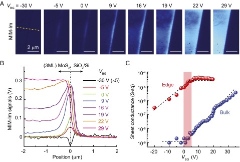
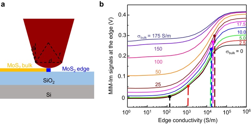
A prominent feature in Fig. 2A is the emergence of conductive edge states before the bulk of the sample is populated by conduction electrons. The presence of localized edge channels on the boundary of a 2D system is one of the most intriguing phenomena in condensed matter physics (37). In the case of TMDs, both density functional theory (DFT) calculations (20–22) and STM measurements (20, 23) have revealed the metallic (semiconducting) states at the zigzag (armchair) edges, whereas their influence on the device performance has not been experimentally probed. The MIM-Im images on the three-ML side of the sample at selected VBG are shown in Fig. 3A, with the line profiles across the sample edge (yellow dashed line) plotted in Fig. 3B. Note that the apparent width of ∼200−300 nm at different locations of the boundary is determined by the spatial resolution or the tip diameter d rather than the actual width wedge of the edge states. To quantify the edge conductance, we performed 3D FEA modeling of the MIM response, in which a narrow conductive channel with wedge = 5 nm is situated in between the insulating substrate and the MoS2 bulk. Because wedge << d, the simulation result is invariant with respect to the product of wedge and the sheet conductance of the edge gedge. Details and justifications of the modeling parameters are shown in Fig. S5. The edge and bulk conductance values determined by comparing the 3D FEA and the MIM data are plotted in Fig. 3C. As VBG increases from −30 V to 0 V, gedge rapidly increases for more than two orders of magnitude, whereas the bulk conductance gbulk stays below our sensitivity limit of ∼10−9 S⋅sq. For 0 V < VBG < 5 V, gedge levels off and gbulk starts to rise above the noise floor. For VBG above 5 V, gedge saturates around 4 × 10⁻⁵ S⋅sq, whereas gbulk continues to increase as VBG increases. The quantitative mapping of gedge signifies the fundamental difference between the topologically trivial edge states in TMDs and the nontrivial quantum Hall (QH) (37) or quantum spin Hall (QSH) (38, 39) edges. The TMD edges in our case can be treated as a normal 1D conductor, where the carriers experience the usual scattering events. Given the FET channel length L ≈ 10 μm in this sample, the maximum contribution of the edge states to the total conduction Gedge = gedge⋅wedge/L is on the order of 10−8 S, which is negligible once the FET is turned on. The QH or QSH edge channels, on the other hand, are dissipationless due to the suppression of backscattering and are responsible for the transport quantization when the bulk is insulating. Indeed, in our previous MIM studies on both QH (30) and QSH (31) systems, the highly conductive edges display maximum MIM-Im and zero MIM-Re signals, in sharp contrast to the finite signals in both channels for the MoS2 edges.
Fig. 3.
Edge state conductance of MoS2. (A) Selected MIM-Im images on the rightmost region of the flake. (Scale bars, 2 μm.) (B) Selected profiles (averaged over 20 lines) along the yellow dashed line in A. The physical boundary of the three-ML MoS2 is centered in the plot. (C) Effective edge and bulk conductance as a function of VBG. The shaded column marks the onset of bulk conduction and the saturation of edge conduction. The dashed lines are guides to the eyes.
Fig. S5.
The 3D FEA modeling for MoS2 with edge states. (A) Schematic of the tip−sample geometry of the 3D modeling. (B) Computed MIM-Im signals of the edge state as a function of the edge conductivity at various bulk conductivity values. Because the width of MoS2 edge states is much smaller than the tip diameter, we can no longer use the 2D axisymmetric model to simulate the edge states. A shows the 3D FEA geometry, in which the MoS2 edge states are modeled as a thin wire with a width of wedge = 5 nm. Note that, although the actual wedge can be anywhere from subnanometer to a few nanometers (23), its exact value is not important here, because the simulation is invariant with respect to gedge⋅wedge. As VBG changes, both the bulk and edge conductivity will change accordingly. Moreover, to deduce the edge conductivity, the bulk conductivity should be first determined from the 2D FEA. B shows a series of simulated MIM-Im curves with different σbulk from 0 S/m to 175 S/m. The edge conductivity σedge at a certain VBG can thus be extracted from the corresponding curve. The sheet conductance of edges (gedge) in Fig. 3C is then calculated as gedge= σedge⋅h, where h = 2 nm is the film thickness.
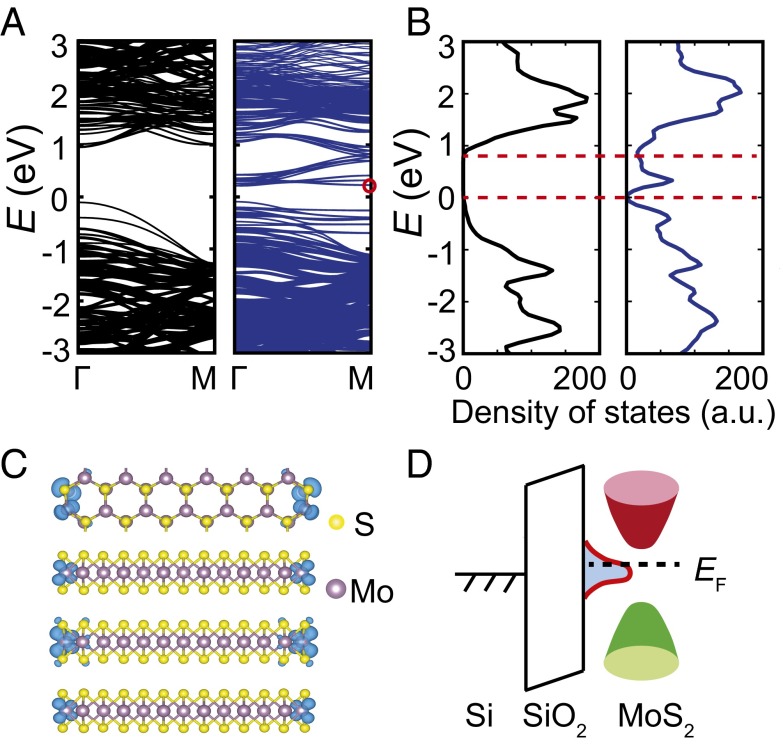
For further investigations of the observed edge states, we carried out first-principles DFT calculations (Methods) on one-ML and three-ML MoS2 nanosheets. Fig. 4A shows the computed energy bands of an infinite 2D sheet and a nanoribbon with armchair edges of three-ML MoS2. Compared with the bulk band structure, multiple bands appear within the bulk gap for the nanoribbon, reducing its energy gap from the bulk value of ∼1.1 eV to ∼0.3 eV, as also indicated by the density of states (DOS) plots in Fig. 4B. The charge density of additional electronic states at the M point of the Brillouin zone, circled in Fig. 4A, is well localized at boundary atoms in Fig. 4C, confirming that the additional bands in Fig. 4A are associated with the edge states. For a nanoribbon with zigzag edges, there are also edge states within the band gap, which connect the bulk conduction and valence bands as shown in Fig. S6 (18–20). For completeness, we have also included the DFT results of one-ML MoS2 in Fig. S6, showing similar characteristics to the three-ML MoS2. In reality, the edges in our devices may be a mixture of armchair and zigzag configurations, and the dangling bonds are usually terminated by foreign molecules from the environment. Nevertheless, the additional DOS inside the bulk band gap will be retained, leading to the topologically trivial edge states at the sample boundary (20, 22). As schematically illustrated in Fig. 4D, electrons will first populate the edge states with increasing VBG. After these in-gap states are completely filled and gedge is saturated, the further increase of VBG will then raise the Fermi level EF into the bulk conduction band, resulting in the upturn of gbulk. Compared with the bulk bands, the edge bands are relatively flat, suggestive of higher effective mass and possibly lower mobility of the edge states. Consequently, once the bulk states participate in the transport at high gate voltages, the contribution of the edge states to the overall conductance becomes negligible. Such a physical picture nicely matches the evolution of local conductance maps deduced from the MIM data in Fig. 3C.
Fig. 4.
DFT calculations of three-layer MoS2 edge states. (A) Calculated band structures of the three-ML bulk MoS2 (Left) and a 1.9-nm-wide MoS2 nanoribbon with armchair edges (Right). (B) Total DOS of the same bulk (Left) and nanoribbon (Right) MoS2. (C) Top view (Uppermost Row) and side view (Lower Three Rows) of the electron wave functions for selected orbitals, circled in A. The edge states are mainly localized at the boundary atoms. (D) Cartoon of edge and bulk band structures. As the Fermi level EF moves upward, the edge states will be populated before the bulk states.
Fig. S6.
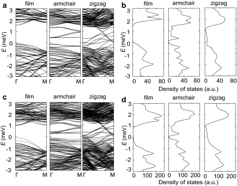
The one-ML and three-ML MoS2 edge states by DFT calculations. (A) Calculated band structures of the one-ML bulk MoS2 (Left), 1.9-nm-wide MoS2 armchair nanoribbons (Middle), and 3.1-nm-wide zigzag nanoribbons (Right). For all of the configurations, the edge atoms are not saturated by extra atoms, as shown in Fig. 4. (B) Corresponding DOS for MoS2 in A. Calculated band structure (C) and corresponding DOS (D) for three-ML MoS2. Compared with bulk band structure, multiple bands emerge within the band gap for both armchair and zigzag nanoribbons. For the armchair nanoribbons, the energy gaps, ∼0.5 eV for one ML and ∼0.3 eV for three ML, are reduced from the bulk values, ∼1.6 eV for one ML and ∼1.1 eV for three ML. In contrast, the edge bands of zigzag nanoribbons seamlessly connect the bulk conduction and valence bands. Note that the SOC is considered for both cases. SOC reduces the degeneracy of energy bands but does not change the main features of band structures (21).
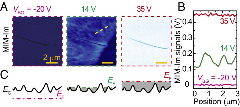
From the onset of bulk conduction at VBG = 5 V to the saturation of MIM signals around VBG = 25 V, pronounced spatial inhomogeneity with submicrometer length scale can be observed inside the MoS2 flake. Both the strengths and spatial dimensions of the conductance fluctuations in this subthreshold regime are of critical importance for the device performance. We emphasize that the large variation of MIM signals cannot be accounted for by the surface roughness of the Al2O3 capping layer, as analyzed in Fig. S7. In Fig. 5A, the zoom-in MIM-Im images are displayed at VBG = −20 V, 14 V, and 35 V, together with the corresponding line profiles in Fig. 5B. The variation of MIM signals at VBG = 14 V corresponds to local fluctuations of gbulk from 5 × 10⁻⁸ S⋅sq to 2 × 10⁻⁷ S⋅sq in the four-ML region. Admittedly, the MIM-Im response (Fig. 2C) is also highly sensitive in this intermediate conductance range. Because the transistor is completely turned off for VBG = −20 V (EF below the bulk conduction band minimum EC) and on for VBG = 35 V (EF well above EC), as shown in Fig. 1C, it is reasonable to expect much weaker spatial conductance variations under these two conditions. On the other hand, electrical inhomogeneity is most significant when EF intersects the spatially fluctuating EC, as schematically shown in Fig. 5C. The MIM maps thus provide both quantitative measurements and direct visualization of the mesoscopic potential landscape in the sample (32), which is the combined effect from defects within the MoS2 layer, charges inside the substrate and the capping layer, and impurities across the interface. The percolation network is vividly demonstrated in the subthreshold regime, which was only indirectly inferred from atomic scale or macroscale studies (18, 19). Note that a similar technique, the alternating current STM (40), can be applied to study the atomic-scale defects in MoS2, which would provide complementary information to our MIM work.
Fig. S7.
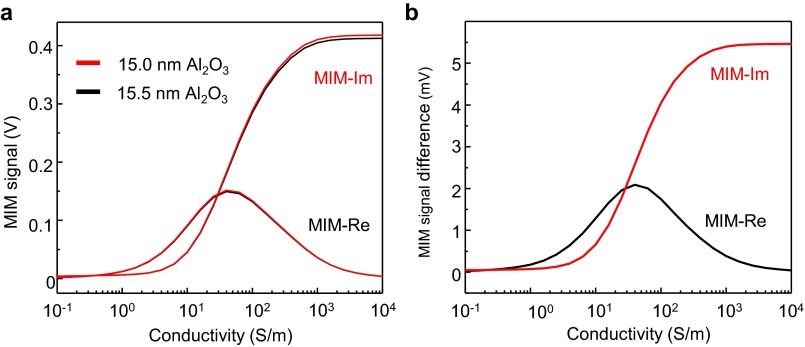
Influence of Al2O3 roughness on MIM signals. (A) Computed MIM signals as a function of the MoS2 conductivity for Al2O3 thicknesses of 15.0 nm and 15.5 nm. (B) Difference between the MIM signals for the two cases in A. The influence of the surface roughness (∼0.4−0.5 nm) of the Al2O3 layer is minimal (<6 mV) and cannot explain the large electrical inhomogeneity observed in the MIM images around the subthreshold regime.
Fig. 5.
Electrical inhomogeneity in the MoS2 FET device. (A) Close-up MIM-Im images in the center of the flake at VBG = −20 V, 14 V, and 35 V. (Scale bars, 2 μm.) (B) Line cuts along the orange dashed line in A at the three VBG as in A. (C) Schematics of the relative positions between EF and the spatially fluctuating EC at the same VBG as in A and B. The color coding (purple, green, and red) matches the solid circles in Fig. 1C.
In summary, we demonstrate the local conductance mapping of functional MoS2 FETs by MIM. We find that, during the insulator-to-metal transition, electrons induced by the electrostatic field effect first populate the edge states before occupying the bulk of the 2D sheets, a scenario further corroborated by our first-principles calculations. The results unambiguously confirm that the contribution of edge states to the channel conductance is significant under the threshold voltage but negligible once the bulk becomes conductive. The magnitude and spatial dimensions of mesoscopic electrical inhomogeneity in the subthreshold regime are also visualized from the MIM data. The simultaneous macroscopic transport and mesoscopic imaging experiments on TMD FETs are critically important for both fundamental research and practical applications on these fascinating materials.
Methods
Transport Measurements.
Output and transfer characteristic curves are measured at the ambient condition with a semiconductor analyzer Keithley 4200.
MIM Measurements.
The MIM in this work is based on an AFM platform (Park AFM XE-70). The customized shielded cantilevers are commercially available from PrimeNano Inc. FEA is performed using the commercial software COMSOL 4.4.
DFT Calculations.
Density functional theory calculations are performed using the Vienna Ab Initio Simulation Package with the projector augmented wave method and Perdew−Burke−Ernzerhof exchange-correlation functional (41–43). For three-ML MoS2, the interlayer van der Waals interactions are taken into account by Grimme's D2 correction (44). A plane wave cutoff of 400 eV and a k-point spacing smaller than 0.2 Å−1 along each periodic direction are used. A vacuum layer of larger than 15 Å is adopted to minimize the interaction between MoS2 nanoribbon/sheet and its periodic images. Atomic structures are fully relaxed, with the force on each atom less than 0.01 eV/Å. The spin−orbit coupling (SOC) is included in the calculation of electronic properties, given a giant spin−orbit-induced spin splitting in MoS2 layers (45). Denser k meshes and a Gaussian smearing of 0.1 eV are applied in the calculation of DOS. For an infinite sheet of one-ML and three-ML MoS2, we construct supercells with a similar structure to corresponding armchair nanoribbons but without edges, which can be easily compared with the results of armchair nanoribbons.
Supplementary Material
Acknowledgments
The MIM work (D.W., L.L., X.W., Z.C. and K.L.) was supported by the US Department of Energy (DOE), Office of Science, Basic Energy Sciences, under Early Career Award DE-SC0010308. D.W. acknowledges support from Welch Foundation Grant F-1814. W.L., M.N.Y., and D.A. acknowledge the support of Office of Naval Research under Contract N00014-1110190 and Nanomanufacturing Systems for Mobile Computing and Energy Technologies (NASCENT) Engineering Research Center under Cooperative Agreement EEC-1160494. Theoretical calculation (X.L. and Q.N.) was supported by China 973 Program (Projects 2013CB921900 and 2012CB921300), DOE (DE-FG03-02ER45958), and Welch Foundation (F-1255).
Footnotes
The authors declare no conflict of interest.
This article is a PNAS Direct Submission. P.S.W. is a Guest Editor invited by the Editorial Board.
This article contains supporting information online at www.pnas.org/lookup/suppl/doi:10.1073/pnas.1605982113/-/DCSupplemental.
References
- 1.Wang QH, Kalantar-Zadeh K, Kis A, Coleman JN, Strano MS. Electronics and optoelectronics of two-dimensional transition metal dichalcogenides. Nat Nanotechnol. 2012;7(11):699–712. doi: 10.1038/nnano.2012.193. [DOI] [PubMed] [Google Scholar]
- 2.Radisavljevic B, Radenovic A, Brivio J, Giacometti V, Kis A. Single-layer MoS2 transistors. Nat Nanotechnol. 2011;6(3):147–150. doi: 10.1038/nnano.2010.279. [DOI] [PubMed] [Google Scholar]
- 3.Zhang Y, Ye J, Matsuhashi Y, Iwasa Y. Ambipolar MoS2 thin flake transistors. Nano Lett. 2012;12(3):1136–1140. doi: 10.1021/nl2021575. [DOI] [PubMed] [Google Scholar]
- 4.Radisavljevic B, Kis A. Mobility engineering and a metal-insulator transition in monolayer MoS₂. Nat Mater. 2013;12(9):815–820. doi: 10.1038/nmat3687. [DOI] [PubMed] [Google Scholar]
- 5.Baugher BWH, Churchill HOH, Yang Y, Jarillo-Herrero P. Intrinsic electronic transport properties of high-quality monolayer and bilayer MoS2. Nano Lett. 2013;13(9):4212–4216. doi: 10.1021/nl401916s. [DOI] [PubMed] [Google Scholar]
- 6.Chen X, et al. Probing the electron states and metal-insulator transition mechanisms in molybdenum disulphide vertical heterostructures. Nat Commun. 2015;6:6088. doi: 10.1038/ncomms7088. [DOI] [PubMed] [Google Scholar]
- 7.Yuan HT, et al. Zeeman-type spin splitting controlled by an electric field. Nat Phys. 2013;9(9):563–569. [Google Scholar]
- 8.Wu SF, et al. Electrical tuning of valley magnetic moment through symmetry control in bilayer MoS2. Nat Phys. 2013;9(3):149–153. [Google Scholar]
- 9.Mak KF, McGill KL, Park J, McEuen PL. Valleytronics. The valley Hall effect in MoS2 transistors. Science. 2014;344(6191):1489–1492. doi: 10.1126/science.1250140. [DOI] [PubMed] [Google Scholar]
- 10.Yuan H, et al. Generation and electric control of spin−valley-coupled circular photogalvanic current in WSe2. Nat Nanotechnol. 2014;9(10):851–857. doi: 10.1038/nnano.2014.183. [DOI] [PubMed] [Google Scholar]
- 11.Zhang YJ, Oka T, Suzuki R, Ye JT, Iwasa Y. Electrically switchable chiral light-emitting transistor. Science. 2014;344(6185):725–728. doi: 10.1126/science.1251329. [DOI] [PubMed] [Google Scholar]
- 12.Lee J, Mak KF, Shan J. Electrical control of the valley Hall effect in bilayer MoS2 transistors. Nat Nanotechnol. 2016;11(5):421–425. doi: 10.1038/nnano.2015.337. [DOI] [PubMed] [Google Scholar]
- 13.Taniguchi K, Matsumoto A, Shimotani H, Takagi H. Electric-field-induced superconductivity at 9.4 K in a layered transition metal disulphide MoS2. Appl Phys Lett. 2012;101(10):042603. [Google Scholar]
- 14.Ye JT, et al. Superconducting dome in a gate-tuned band insulator. Science. 2012;338(6111):1193–1196. doi: 10.1126/science.1228006. [DOI] [PubMed] [Google Scholar]
- 15.Saito Y, et al. Superconductivity protected by spin−valley locking in ion-gated MoS2. Nat Phys. 2016;12(2):144–149. [Google Scholar]
- 16.Ghatak S, Pal AN, Ghosh A. Nature of electronic states in atomically thin MoS2 field-effect transistors. ACS Nano. 2011;5(10):7707–7712. doi: 10.1021/nn202852j. [DOI] [PubMed] [Google Scholar]
- 17.Qiu H, et al. Hopping transport through defect-induced localized states in molybdenum disulphide. Nat Commun. 2013;4:2642. doi: 10.1038/ncomms3642. [DOI] [PubMed] [Google Scholar]
- 18.Komsa HP, et al. Two-dimensional transition metal dichalcogenides under electron irradiation: Defect production and doping. Phys Rev Lett. 2012;109(3):035503. doi: 10.1103/PhysRevLett.109.035503. [DOI] [PubMed] [Google Scholar]
- 19.Parkin WM, et al. Raman shifts in electron-irradiated monolayer MoS2. ACS Nano. 2016;10(4):4134–4142. doi: 10.1021/acsnano.5b07388. [DOI] [PMC free article] [PubMed] [Google Scholar]
- 20.Bollinger MV, et al. One-dimensional metallic edge states in MoS2. Phys Rev Lett. 2001;87(19):196803. doi: 10.1103/PhysRevLett.87.196803. [DOI] [PubMed] [Google Scholar]
- 21.Li Y, Zhou Z, Zhang S, Chen Z. MoS2 nanoribbons: High stability and unusual electronic and magnetic properties. J Am Chem Soc. 2008;130(49):16739–16744. doi: 10.1021/ja805545x. [DOI] [PubMed] [Google Scholar]
- 22.Xiao J, et al. Carrier mobility of MoS2 nanoribbons with edge chemical modification. Phys Chem Chem Phys. 2015;17(10):6865–6873. doi: 10.1039/c4cp05199h. [DOI] [PubMed] [Google Scholar]
- 23.Zhang C, Johnson A, Hsu CL, Li LJ, Shih CK. Direct imaging of band profile in single layer MoS2 on graphite: Quasiparticle energy gap, metallic edge states, and edge band bending. Nano Lett. 2014;14(5):2443–2447. doi: 10.1021/nl501133c. [DOI] [PubMed] [Google Scholar]
- 24.Lai K, Kundhikanjana W, Kelly M, Shen ZX. Modeling and characterization of a cantilever-based near-field scanning microwave impedance microscope. Rev Sci Instrum. 2008;79(6):063703. doi: 10.1063/1.2949109. [DOI] [PubMed] [Google Scholar]
- 25.Lai K, Kundhikanjana W, Kelly M, Shen ZX. Nanoscale microwave microscopy using shielded cantilever probes. Appl Nanosci. 2011;1(1):13–18. [Google Scholar]
- 26.Yang YL, et al. Batch-fabricated cantilever probes with electrical shielding for nanoscale dielectric and conductivity imaging. J Micromech Microeng. 2012;22(11):115040. [Google Scholar]
- 27.Yuan H, et al. Influence of metal-MoS2 interface on MoS2 transistor performance: Comparison of Ag and Ti contacts. ACS Appl Mater Interfaces. 2015;7(2):1180–1187. doi: 10.1021/am506921y. [DOI] [PubMed] [Google Scholar]
- 28.Chang H-Y, et al. Large-area monolayer MoS2 for flexible low-power RF nanoelectronics in the GHz regime. Adv Mater. 2016;28(9):1818–1823. doi: 10.1002/adma.201504309. [DOI] [PubMed] [Google Scholar]
- 29.Lai K, Ji MB, Leindecker N, Kelly MA, Shen ZX. Atomic-force-microscope-compatible near-field scanning microwave microscope with separated excitation and sensing probes. Rev Sci Instrum. 2007;78(6):063702. doi: 10.1063/1.2746768. [DOI] [PubMed] [Google Scholar]
- 30.Lai K, et al. Imaging of Coulomb-driven quantum Hall edge states. Phys Rev Lett. 2011;107(17):176809. doi: 10.1103/PhysRevLett.107.176809. [DOI] [PubMed] [Google Scholar]
- 31.Ma EY, et al. Unexpected edge conduction in mercury telluride quantum wells under broken time-reversal symmetry. Nat Commun. 2015;6:7252. doi: 10.1038/ncomms8252. [DOI] [PMC free article] [PubMed] [Google Scholar]
- 32.Ren Y, et al. Direct imaging of nanoscale conductance evolution in ion-gel-gated oxide transistors. Nano Lett. 2015;15(7):4730–4736. doi: 10.1021/acs.nanolett.5b01631. [DOI] [PubMed] [Google Scholar]
- 33.Kaasbjerg K, Thygesen KS, Jacobsen KW. Phonon-limited mobility in n-type single-layer MoS2 from first principles. Phys Rev B. 2012;85(11):115317. [Google Scholar]
- 34.Splendiani A, et al. Emerging photoluminescence in monolayer MoS2. Nano Lett. 2010;10(4):1271–1275. doi: 10.1021/nl903868w. [DOI] [PubMed] [Google Scholar]
- 35.Das S, Chen HY, Penumatcha AV, Appenzeller J. High performance multilayer MoS2 transistors with scandium contacts. Nano Lett. 2013;13(1):100–105. doi: 10.1021/nl303583v. [DOI] [PubMed] [Google Scholar]
- 36.Berweger S, et al. Microwave near-field imaging of two-dimensional semiconductors. Nano Lett. 2015;15(2):1122–1127. doi: 10.1021/nl504960u. [DOI] [PubMed] [Google Scholar]
- 37.Halperin BI. Quantized Hall conductance, current-carrying edge states, and the existence of extended states in a two-dimensional disordered potential. Phys Rev B. 1982;25(4):2185–2190. [Google Scholar]
- 38.Kane CL, Mele EJ. Z2 topological order and the quantum spin Hall effect. Phys Rev Lett. 2005;95(14):146802. doi: 10.1103/PhysRevLett.95.146802. [DOI] [PubMed] [Google Scholar]
- 39.Bernevig BA, Zhang SC. Quantum spin Hall effect. Phys Rev Lett. 2006;96(10):106802. doi: 10.1103/PhysRevLett.96.106802. [DOI] [PubMed] [Google Scholar]
- 40.Weiss PS, McCarty GS. 2003. US Patent 6,597,194 B2.
- 41.Kresse G, Furthmüller J. Efficient iterative schemes for ab initio total-energy calculations using a plane-wave basis set. Phys Rev B Condens Matter. 1996;54(16):11169–11186. doi: 10.1103/physrevb.54.11169. [DOI] [PubMed] [Google Scholar]
- 42.Perdew JP, Burke K, Ernzerhof M. Generalized gradient approximation made simple. Phys Rev Lett. 1996;77(18):3865–3868. doi: 10.1103/PhysRevLett.77.3865. [DOI] [PubMed] [Google Scholar]
- 43.Kresse G, Joubert D. From ultrasoft pseudopotentials to the projector augmented-wave method. Phys Rev B. 1999;59(3):1758–1775. [Google Scholar]
- 44.Grimme S. Semiempirical GGA-type density functional constructed with a long-range dispersion correction. J Comput Chem. 2006;27(15):1787–1799. doi: 10.1002/jcc.20495. [DOI] [PubMed] [Google Scholar]
- 45.Zhu ZY, Cheng YC, Schwingenschlogl U. Giant spin-orbit-induced spin splitting in two-dimensional transition-metal dichalcogenide semiconductors. Phys Rev B. 2011;84(15):153402. [Google Scholar]
- 46.Liu Y, et al. Mesoscale imperfections in MoS2 atomic layers grown by a vapor transport technique. Nano Lett. 2014;14(8):4682–4686. doi: 10.1021/nl501782e. [DOI] [PubMed] [Google Scholar]
- 47.Molina-Sanchez A, Wirtz L. Phonons in single-layer and few-layer MoS2 and WS2. Phys Rev B. 2011;84(15):155413. [Google Scholar]
Associated Data
This section collects any data citations, data availability statements, or supplementary materials included in this article.


