Abstract
The direct band gap of monolayer semiconducting transition-metal dichalcogenides (STMDs) enables a host of new optical and electrical properties. However, bilayer STMDs are indirect band gap semiconductors, which limits its applicability for high-efficiency optoelectronic devices. Here, we report that the direct band gap can be achieved in bilayer MoSe2-WSe2 lateral heterostructures by alternating stacking orders. Specifically, when Se atoms from opposite layers are stacked directly on top of each other, AA and A’B stacked heterostructures show weaker interlayer coupling, larger interlayer distance and direct band gap. Whereas, when Se atoms from opposite layers are staggered, AA’, AB and AB’ stacked heterostructures exhibit stronger interlayer coupling, shorter interlayer distance and indirect band gap. Thus, the direct/indirect band gap can be controllable in bilayer MoSe2-WSe2 lateral heterostructures. In addition, the calculated sliding barriers indicate that the stacking orders of bilayer MoSe2-WSe2 lateral heterostructures can be easily formed by sliding one layer with respect to the other. The novel direct band gap in bilayer MoSe2-WSe2 lateral heterostructures provides possible application for high-efficiency optoelectronic devices. The results also show that the stacking order is an effective strategy to induce and tune the band gap of layered STMDs.
Compared with gapless graphene1,2, two-dimensional (2D) STMDs have attracted great interest because of its sizeable band gap3,4,5,6,7. Monolayer STMDs (MX2; M = Mo, W and X = S, Se, Te) is composed of three atomic layers, a transition-metal layer sandwiched between two chalcogen layers. Within monolayer the metals and chalcogens form strong covalent bonds, whereas in bulk STMDs, the layers are bonded by the weak van der Waals (vdW) interaction. Because of the strong intralayer interaction and the weak interlayer interaction, the ultrathin sheets of STMDs can be isolated from the bulk by the micromechanical cleavage technique8. The direct band gap of monolayer STMDs enables a host of new optical and electrical properties, such as strong photoluminescence9,10 and electroluminescence11. Novel electronic and optoelectronic devices with improved performance have also been demonstrated, such as ambipolar and high-quality field-effect transistors12,13, electric double-layer transistors14, integrated circuits15 and phototransistors with high responsivity16,17. However, experimentally it is still a challenge to precisely control layer number of STMDs, the synthesized samples are usually several layer thickness. The multilayer STMDs are indirect band gap semiconductors9,10, which limits its applicability for high-performing optoelectronic devices. If the electronic properties can be tuned from the indirect band gap to the direct band gap, they will be quite promising for practical application.
Bilayer STMDs have received much attention because they possess extra and distinct degrees of freedom, such as heterostructures and stacking orders, which makes bilayer STMDs exhibiting richer properties. Heterostructures have been the essential elements in modern semiconductor industry due to its electronic properties beyond those offered by individual constituent parts. Creating heterostructures between 2D STMDs would enable band engineering and provide new strategy to tune the electronic properties of semiconductors. Advances in 2D layered materials have allowed STMDs-based vertical and lateral heterostructures to be fabricated18,19,20,21,22 and meanwhile interesting physical properties have been explored on such 2D heterostructures23,24,25,26,27. For example, MoS2/WSe2 stacked heterostructure can form a type-II heterojunction19. A strong interlayer excitonic transition was observed in WS2/MoS2 vertical heterostructures20 and it showed a smaller band gap than the ones of WS2 and MoS2 monolayers23. The excellent current rectification behavior and photocurrent generation characteristic was found in WSe2-WS2 lateral heterojunctions21. Monolayer MoSe2-WSe2 lateral heterostructures have been achieved experimently and demonstrated enhanced photoluminescence22.
On the other hand, stacking faults are common in the layered materials because the energy barrier of different stacking orders is usually small, so that the sliding of layers can occur. This phenomenon has wide application in solid lubricants, such as h-BN nano-sheets28 or WS2 nanotubes29. The 2D nature of layered STMDs provides a unique opportunity to engineer their electronic properties by stacking monolayers in different ways3,30,31,32. Very recently, MoS2 bilayers with different stacking orders have been obtained by folding exfoliated monolayers experimentally, where the stacking dependent electronic properties are demonstrated30. In addition, Terrones et al. reported the possibility of direct band gap by assembling different layers of STMDs with particular stackings31. He et al. demonstrated that the electronic and optical properties of bilayer STMDs were affected by stacking orders32. All of these findings suggest that the heterostructure and stacking orders may offer new physical properties for layered STMDs.
Motivated by the successful fabrication and enhanced photoluminescence demonstrated in monolayer MoSe2-WSe2 lateral heterostructure22, we first performed first principles calculations on the electronic properties of monolayer MoSe2-WSe2 lateral heterostructure, and found the character of a direct band gap. Then we stacked additional same layer on monolayer MoSe2-WSe2 lateral heterostructures and investigated the stacking orders induced modification on the electronic properties of bilayer MoSe2-WSe2 lateral heterostructures. The direct band gap can be achieved in bilayer MoSe2-WSe2 lateral heterostructures by alternating stacking orders. Specifically, AA and A’B stacked heterostructures show weaker interlayer coupling, larger interlayer distance and direct band gap. Whereas AA’, AB and AB’ stacked heterostructures exhibit stronger interlayer coupling, shorter interlayer distance and indirect band gap. The novel direct band gap in bilayer MoSe2-WSe2 lateral heterostructures provides possible application for high-efficiency optoelectronic devices. In addition, the calculated sliding barriers indicate that stacking orders of bilayer MoSe2-WSe2 lateral heterostructures can be easily formed by sliding one layer with respect to the other. The results suggest that the feasibility of stacking orders in tuning the electronic properties of layered STMDs.
Results
Structural and Electronic Properties of Monolayer MoSe2-WSe2 Lateral Heterostructures
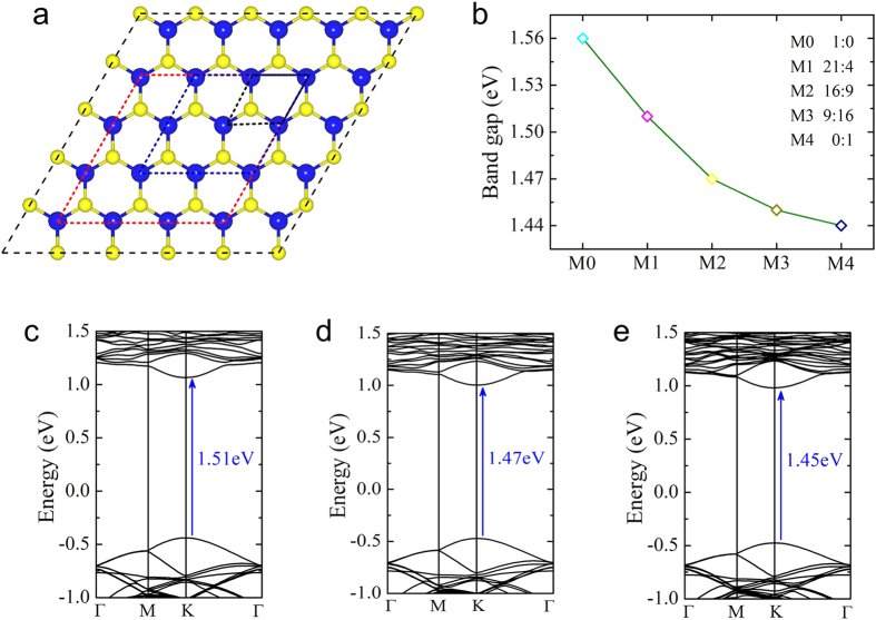
In order to compare the band structures of monolayer and bilayer MoSe2-WSe2 lateral heterostructures, we first examined the lattice constants and band structures of monolayer MoSe2-WSe2 lateral heterostructures. The optimized values of lattice constants are found to be 3.316 Å (WSe2) and 3.319 Å (MoSe2), well consistent with previously reported results33. Because the lattice constants of WSe2 and MoSe2 are very close, monolayer MoSe2-WSe2 lateral heterostructures can be constructed simply from the primitive cells of WSe2 and MoSe2 with negligible strain. A 5 × 5 supercell of WSe2 is shown in Fig. 1a. Monolayer MoSe2-WSe2 lateral heterostructures can be obtained by replacing WSe2 with MoSe2 at the rhombic area. The dashed line rhombuses with different sizes stand for the replaced area. Note that the regular doping in monolayer MoSe2-WSe2 lateral heterostructures have been achieved experimently22, different from random doping in transition metal dichalcogenide alloys34,35. Here, we consider three monolayer MoSe2-WSe2 lateral heterostructures by varying the WSe2 to MoSe2 ratio (21:4, 16:9 and 9:16), corresponding to the small, middle and big rhombuses in Fig. 1a. For simplified, the three different ratio monolayer heterostructures are named as M1, M2 and M3, and the homogeneous WSe2 and MoSe2 are denoted as M0 and M4, shown in Fig. 1b. It is seen from Fig. 1b that the band gaps of monolayer MoSe2-WSe2 lateral heterostructures can be tuned from 1.51, 1.47 to 1.45 eV as the ratio of WSe2 to MoSe2 decreases, which are between the band gaps of homogeneous WSe2 (1.56 eV) and MoSe2 (1.44 eV). The three different WSe2/MoSe2 ratio heterostructures all exhibit a direct band gap with the valence band maximum (VBM) and conduction band minimum (CBM) located at the K point (see Fig. 1c–e). Similar to the homogeneous monolayer STMDs, monolayer MoSe2-WSe2 lateral heterostructures show the direct band gap regardless of the WSe2/MoSe2 ratio.
Figure 1.
(a) The structural models of monolayer MoSe2-WSe2 lateral heterostructures. The dashed line rhombuses stand for the replaced MoSe2. The blue and yellow balls represent W and Se atoms, respectively. (b) The band gaps as a function of the WSe2 to MoSe2 ratio. (c–e) Band structures of monolayer MoSe2-WSe2 lateral heterostructures in the case of M1, M2 and M3.
Stacking Orders Induced Modification on the Electronic Properties of Bilayer MoSe2-WSe2 Lateral Heterostructures
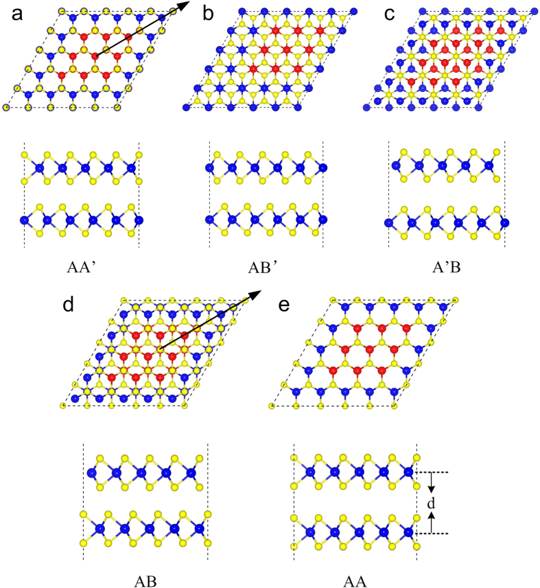
The direct band gap only occurs in monolayer STMDs, the tunable electronic properties and the direct gap in bilayer STMDs are desirable. The 2D nature of layered STMDs provides a unique opportunity to engineer their electronic properties by stacking monolayers in different ways3. Here, we stacked additional same layer on monolayer MoSe2-WSe2 lateral heterostructures. Corresponding to the WSe2/MoSe2 ratio in monolayer MoSe2-WSe2 lateral heterostructures (M1, M2 and M3), similarly, the three different ratio bilayer MoSe2-WSe2 lateral heterostructures are named as B1, B2 and B3. The five different stacking orders in bilayer MoSe2-WSe2 lateral heterostructures are proposed. Taking B2 as an example, the five high-symmetry stacking orders are depicted in Fig. 2a–e. (i) AA’ (eclipsed with W (Mo) over Se, the characteristic of the 2H phase); (ii) AB’ (staggered with W (Mo) over W (Mo)); (iii) A’B (staggered with Se over Se); (iv) AB (staggered with Se over W (Mo), the characteristic of the 3R phase); (v) AA (eclipsed with W (Mo) over W (Mo) and Se over Se). The different stacking orders can be obtained by sliding of the top layer with respect to the bottom layer: sliding from the AA’ stacking order through the AB’ to the A’B stacking order along the arrow direction in Fig. 2a, or sliding from the AB stacking order to the AA stacking order along the arrow direction in Fig. 2d.
Figure 2. The top and side views of high-symmetry stacking orders in bilayer MoSe2-WSe2 lateral heterostructures.
The arrows denote the sliding direction of the top layer in (a,d). The definition for the interlayer distance d is indicated in (e). The blue, yellow and red balls represent W, Se and Mo atoms, respectively.
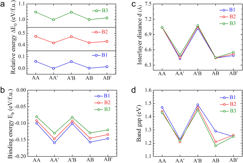
The relative stability of bilayer MoSe2-WSe2 lateral heterostructures was estimated and compared. It is evident from the relative energies of Fig. 3a that the three bilayer MoSe2-WSe2 lateral heterostructures exhibit a very similar behavior in the different stacking orders. Taking the case of B2 as an example, the lowest-energy stacking order is AA’, closely followed by the AB stacking, the latter is only by 2 meV per formula unit (f.u.) less stable than the former. The next stable stacking order is AB’, by 13 meV/f.u. less stable than the AA’ stacking. The remaining other two high-symmetry stackings, AA and A’B, are significantly less stable, which are 56 or 54 meV/f.u. higher than AA’ stacking, respectively. The relative stability of the other WSe2/MoSe2 ratio bilayer heterostructures (B1 and B3 cases) has the same trend.
Figure 3.
(a) The relative energies ΔE0 (eV/f.u., with respect to the lowest-energy stacking order AA’). (b) The binding energy Eb (eV/f.u.) of bilayer MoSe2-WSe2 lateral heterostructures. (c) The optimized interlayer distance d (Å). (d) Band gaps of bilayer MoSe2-WSe2 lateral heterostructures in the different stacking orders.
In order to further confirm the stability of these systems, we calculated the binding energies of bilayer MoSe2-WSe2 lateral heterostructures to quantitatively characterize the binding strength between interlayer. The binding energy is defined as the energy difference between bilayer heterostructures and the corresponding monolayers (Eb = Ebi − Emono1 − Emono2). Results shown in Fig. 3b reveal that the binding energy of bilayer MoSe2-WSe2 lateral heterostructures strongly depends on the stacking orders. It is clear that the binding of AA’ and AB stacked heterostructures are obviously stronger than that of the other stacked ones. Comparing the structures in Fig. 2a,d, W (Mo) and Se atoms from opposite layers sit on top of each other in both AA’ and AB stacked heterostructures, leading to stronger interlayer coupling. Among the others, A’B and AA stacked heterostructures (Fig. 2c,e) have negatively charged Se atoms stacked directly on top of each other. By Coulomb repulsion, their interlayer distance is enlarged and the coupling is reduced. It is found from Fig. 3c that the interlayer distance d is significantly larger in AA (7.04 Å) and A’B (7.06 Å) stacked heterostructures compared to AA’ (6.44 Å) and AB (6.44 Å) stacked ones. Accordingly, the interlayer coupling strength of the different stacked heterostructures is AA’≈ AB > AB’ > AA ≈ A’B, depending on the relative atomic positions of the top layer with respect to the bottom layer.
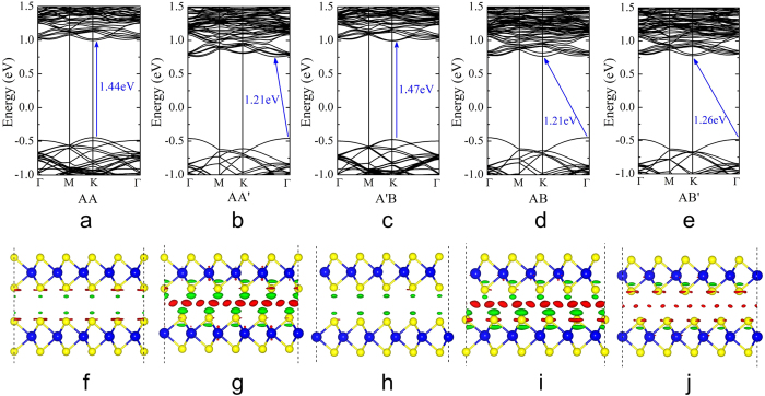
The different stacking orders and interlayer interaction are expected to have significant effect on the electronic properties of bilayer MoSe2-WSe2 lateral heterostructures. As shown in Fig. 3d, the band gaps of bilayer MoSe2-WSe2 lateral heterostructures are quite insensitive to the WSe2/MoSe2 ratio. However, we can see the obvious role of the stacking orders on their electronic properties. The band gap values of AA and A’B stacked heterostructures are significantly larger compared with those of the other stacked heterostructures (see Fig. 3d). This intriguing electronic modulation arises from the larger difference of interlayer distances induced by the different stacking orders. Taking the case of B2 as an example, band structures of the different stacked heterostructures are compared in Fig. 4a–e. It can be classified to two types: (i) AA and A’B stacked heterostructures. It is interesting to note that a direct gap behavior at the K point is observed for AA and A’B stacking orders in bilayer MoSe2-WSe2 lateral heterostructures. The direct gap changes very little, from 1.44 eV (AA stacking) to 1.47 eV (A’B stacking), which are indicated by blue arrows in Fig. 4a,c. The direct gap behavior here is distinctive from the indirect gap in the homogeneous bilayer WSe2 or MoSe2, thus widening the possibilities of applications for bilayer STMDs in the optoelectronic area. (ii) AA’, AB and AB’ stacked heterostructures. The indirect gap behavior is obtained for AA’, AB and AB’ stacking orders. The band gaps changes from 1.21 eV (AA’ and AB stackings, see Fig. 4b,d) to 1.26 eV (AB’ stacking, see Fig. 4e). The VBM is located at the Γ point, whereas the CBM switches from T point (the midpoint between Γ and K) to the K point, resulting in different types of indirect band gaps.
Figure 4.
Band structures (a–e) and charge transfer (f–j) of AA, AA’, A’B, AB, and AB’ stacked bilayer MoSe2-WSe2 lateral heterostructures in the case of B2. The isosurface value for all of the cases is 2 × 10⁻⁴ e/Å3. The red isosurface indicates an electron gain, while the green one represents an electron loss.
From the above analysis, we can summarize the five stacking orders of bilayer MoSe2-WSe2 lateral heterostructures into two classes from the interlayer coupling, binding energies and electronic properties, namely class I (AA and A’B stacking orders) and class II (AA’, AB and AB’ stacking orders). Class I has weaker interlayer coupling/larger interlayer distance and direct band gap, whereas class II has stronger interlayer coupling, shorter interlayer distance and indirect band gap. In addition, in stark contrast, the band gap of class I is larger than that of class II. The origin of the difference is due to the larger interlayer distances in class I as compared to class II, which are d = 7.04 Å and 6.44 Å for AA and AA’ stacked heterostructures respectively (see Fig. 3c). These conclusions can be further supported by the charge transfer, which is defined as the difference of the total charge of bilayer heterostructures and two monolayers (Δρ = ρtot − ρmono1 − ρmono2), as shown in Fig. 4(f–j). As expected, for AA and A’B stacked heterostructures, the small amount of charge transfer was observed, indicating the weak interaction between two monolayers. In comparison to the band gap (1.47 eV) of the corresponding monolayer MoSe2-WSe2 lateral heterostructures (see Fig. 1d), the band gap of AA (1.44 eV) and A’B (1.47 eV) stacked heterostructures are almost completely unaffected. As for AA’, AB and AB’ stacked heterostructures, increasing charge transfer happens, suggesting an enhanced interaction between two monolayers, which essentially causes the band gap decrease. The same trends are also observed in the other ratio bilayer MoSe2-WSe2 lateral heterostructures (see the Supporting Information Figures S1 and S2).
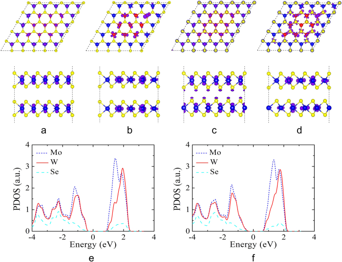
In order to get insight into the origin of the direct and indirect band gap in different stacked heterostructures, we analyze deeply the charge distribution of the VBM and CBM states at the K point of the AA (class I) and AA’ (class II) stacked heterostructures. We present in Fig. 5 the charge densities of the VBM and CBM states and the partial density of states (PDOS) for AA and AA’ stacked heterostructures. For AA stacked heterostructure, the results indicate that the VBM state is dominated by the state from the W and Mo atoms, which are distributed throughout the whole heterostructure, see Fig. 5a. In sharp contrast, the CBM state only originates from the Mo atoms and localized on the MoSe2 part, see Fig. 5b. The analysis is further demonstrated by the PDOS of the W and Mo atoms in AA stacked heterostructure, as shown in Fig. 5e. It is clear that the VBM state is due to the W and Mo atoms, but the CBM state is owed to the Mo atoms. The physical information from PDOS is consistent with those from charge density distribution, which further verify our conclusion. For AA’ stacked heterostructure, it is found that the charge density distribution is very similar to those of AA stacked heterostructure. But from side view of the charge distribution, some obvious difference between AA and AA’ stacked heterostructures can be observed. There is no charge density overlap in AA stacked heterostructure (see Fig. 5a) due to its larger interlayer distance (7.04 Å). The large interlayer distance of AA stacked heterostructure leads to the weak coupling/interaction between the two monolayers, so the band structure of AA stacked heterostructure can be simply regarded as the superposition of these two monolayers. The conclusion can be verified when we compare the band structure in Fig. 1d with that in Fig. 4a. However, the distinct charge density overlap between the interlayer is found in AA’ stacked heterostructure (see Fig. 5c) because of its smaller interlayer distance (6.44 Å), which results in the strong interlayer interaction. That leads to the energy variation of the VBM state (K point) (see Fig. 4b), so the direct band gap transfers into the indirect band gap from AA to AA’ stacked heterostructures. Our results reveal the physical reasons of the direct and indirect band gap for the different stacking orders in bilayer MoSe2-WSe2 lateral heterostructures. Here, the controllable direct/indirect band gap provides new opportunities for engineering the electronic properties of bilayer STMDs. Moreover, the novel direct band gap in bilayer MoSe2-WSe2 lateral heterostructures can be used to achieve the strong photoluminescence and provides possible application in optoelectronic devices.
Figure 5.
The charge densities of (a) VBM, (b) CBM, (e) PDOS of AA stacked, and (c) VBM, (d) CBM, (f) PDOS of AA’ stacked bilayer MoSe2-WSe2 lateral heterostructures in the case of B2. The isosurface value is set to be 0.001e/Å3.
Sliding Barrier of Different Stacking Orders in Bilayer MoSe2-WSe2 Lateral Heterostructures
The above results demonstrated that the structural stability of bilayer MoSe2-WSe2 lateral heterostructures are significantly sensitive to the stacking orders and their electronic properties can widely be tuned from direct to indirect band gap. The weak vdW interaction between interlayer makes it susceptible to stacking in the layered materials. The energy barrier of different stacking orders is usually small, so that the sliding of one layer with respect to the other can occur. In order to understand the sliding behavior in bilayer MoSe2-WSe2 lateral heterostructures, taking the case of B2 as an example, we further carried out the sliding barrier calculations for bilayer MoSe2-WSe2 lateral heterostructures. The sliding barriers were evaluated using the same approach for bilayer BN36,37 and MoX2 (X = S, Se, Te)38. A set of lateral shifts of one layer with respect to the other layer were performed. At each shifted configuration we calculate the total energy of the bilayer heterostructures. Note that the interlayer distance is fixed at 6.44 Å in this set of calculations, starting from the low-energy stacking orders (AA’ and AB). The calculated sliding barriers between different stacking orders are 0.10 eV, 0.12 eV, 0.13 eV per formula unit from AB’ to A’B, AA’ to A’B, AB to AA, respectively, presented in Fig. 6. The result demonstrated that the sliding barrier of different stacking orders is small enough, which indicates that stacking orders of bilayer MoSe2-WSe2 lateral heterostructures can be easily formed by sliding one layer with respect to the other. Experimentally, bilayer MoSe2-WSe2 lateral heterostructures with AA’, AB and AB’ stackings are possible and observed in the bilayer regions of the samples. While less stable AA and A’B stackings can be obtained by folding monolayer or sliding one layer with respect to the other artificially. The recent experimental work30 has shown that MoS2 bilayers with different stacking orders can be produced by folding MoS2 monolayer. Our results provide a feasible strategy to obtain artificial STMDs bilayers by sliding.
Figure 6. The sliding barriers of the different stacked bilayer MoSe2-WSe2 lateral heterostructures in the case of B2.
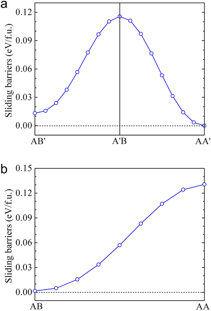
The total energies of AA’ stacking are set to be zero as references, marked by a dotted line.
Discussion
We investigated the stacking orders induced modification on the electronic properties of bilayer MoSe2-WSe2 lateral heterostructures. The direct band gap can be achieved in bilayer MoSe2-WSe2 lateral heterostructures by alternating stacking orders. Specifically, the five stacking orders of bilayer MoSe2-WSe2 lateral heterostructures can be summarized into class I (AA and A’B stacking orders) and class II (AA’, AB and AB’ stacking orders) from the interlayer coupling, binding energies and electronic properties. Class I shows weaker interlayer coupling, larger interlayer distance and direct band gap, whereas class II exhibits stronger interlayer coupling, shorter interlayer distance and indirect band gap. The results elucidated the importance of stacking orders in controllably tuning the band gap of bilayer MoSe2-WSe2 lateral heterostructures, suggesting that the stacking orders is an effective strategy to induce and tune the band gap of layered STMDs. The novel direct band gap in bilayer MoSe2-WSe2 lateral heterostructures provides a promising candidate for applications in optoelectronic devices.
Methods
Our calculations were performed using plane-wave density functional theory (DFT), as implemented in the VASP package39,40. The projector-augmented-wave (PAW) potentials were used to account electron-ion interactions41,42, while the electron exchange-correlation interactions were treated using generalized gradient approximation (GGA) in the scheme of Perdew-Burke-Ernzerhof (PBE)43. Van der Waals corrections were included through Grimme’s DFT-D2 method as implemented in VASP44,45. A kinetic energy cutoff was set to 500 eV. The atomic positions were relaxed until forces were converged to less than 0.02 eV/Å. A k-point sampling of 9 × 9 × 1 was used for the structural relaxations, and a vacuum region of 17 Å was introduced to avoid interaction between periodic images of slabs.
Additional Information
How to cite this article: Hu, X. et al. Stacking orders induced direct band gap in bilayer MoSe2-WSe2 lateral heterostructures. Sci. Rep. 6, 31122; doi: 10.1038/srep31122 (2016).
Supplementary Material
Acknowledgments
This work is supported by the National Natural Science Foundation of China (Nos. 61274114, 51420105003, 11327901 and 11525415), the Natural Science Foundation of Jiangsu Province (No. BK20160694), and China Postdoctoral Science Foundation (No. 2014M561549).
Footnotes
Author Contributions X.H. proposed the idea, performed calculations and wrote the manuscript. L.K. and L.S. discussed the results, contributed with ideas and revised the paper.
References
- Castro Neto A. H., Guinea F., Peres N. M. R., Novoselov K. S. & Geim A. K. The electronic properties of graphene. Rev. Mod. Phys. 81, 109–162 (2009). [Google Scholar]
- Rao C. N. R., Sood A. K., Subrahmanyam K. S. & Govindaraj A. Graphene: the new two-dimensional nanomaterial. Angew. Chem. Int. Ed. 48, 7752–7777 (2009). [DOI] [PubMed] [Google Scholar]
- Geim A. K. & Grigorieva I. V. Van der Waals heterostructures. Nature 499, 419–425 (2013). [DOI] [PubMed] [Google Scholar]
- Editorial. Chalcogenides fill the gap. Nat. Mater. 13, 1073 (2014). [DOI] [PubMed]
- Ma Y., Kou L., Li X., Dai Y., Smith S. C. & Heine T. Quantum spin Hall effect and topological phase transition in two-dimensional square transition-metal dichalcogenides. Phys. Rev. B 92, 085427 (2015). [Google Scholar]
- Ma Y., Kou L., Li X., Dai Y. & Heine T. Two-dimensional transition metal dichalcogenides with a hexagonal lattice: Room-temperature quantum spin Hall insulators. Phys. Rev. B 93, 035442 (2016). [Google Scholar]
- Ma Y., Dai Y., Wei W., Niu C., Yu L. & Huang B. First-principles study of the graphene@MoSe2 heterobilayers. J. Phys. Chem. C 115, 20237–20241 (2011). [Google Scholar]
- Novoselov K. S. et al. Two-dimensional atomic crystals. Proc. Natl. Acad. Sci.USA 102, 10451–10453 (2005). [DOI] [PMC free article] [PubMed] [Google Scholar]
- Splendiani A. et al. Emerging photoluminescence in monolayer MoS2. Nano Lett. 10, 1271–1275 (2010). [DOI] [PubMed] [Google Scholar]
- Mak K. F., Lee C., Hone J., Shan J. & Heinz T. F. Atomically thin MoS2: a new direct-gap semiconductor. Phys. Rev. Lett. 105, 136805 (2010). [DOI] [PubMed] [Google Scholar]
- Sundaram R. S. et al. Electroluminescence in single layer MoS2. Nano Lett. 13, 1416 (2013). [DOI] [PubMed] [Google Scholar]
- Podzorov V., Gershenson M. E., Kloc C., Zeis R. & Bucher E. High-mobility field-effect transistors based on transition metal dichalcogenides. Appl. Phys. Lett. 84, 3301 (2004). [Google Scholar]
- Radisavljevic B. & Kis A. Mobility engineering and a metal-insulator transition in monolayer MoS2. Nat. Mater. 12, 815–820 (2013). [DOI] [PubMed] [Google Scholar]
- Zhang Y. J., Ye J. T., Yomogida Y., Takenobu T. & Iwasa Y. Formation of a stable p-n junction in a liquid-gated MoS2 ambipolar transistor. Nano Lett. 13, 3023–3028 (2013). [DOI] [PubMed] [Google Scholar]
- Wang H. et al. Integrated circuits based on bilayer MoS2 transistors. Nano Lett. 12, 4674–4680 (2012). [DOI] [PubMed] [Google Scholar]
- Yin Z. et al. Single-layer MoS2 phototransistors. ACS Nano 6, 74–80 (2012). [DOI] [PubMed] [Google Scholar]
- Lopez-Sanchez O., Lembke D., Kayci M., Radenovic A. & Kis A. Ultrasensitive photodetectors based on monolayer MoS2. Nat. Nanotechnol. 8, 497–501 (2013). [DOI] [PubMed] [Google Scholar]
- Shi S. & Wang F. Atomically thin p-n junctions. Nat. Nanotechnol. 9, 664–665 (2014). [DOI] [PubMed] [Google Scholar]
- Lee C. et al. Atomically thin p-n junctions with van der Waals heterointerfaces. Nat. Nanotechnol. 9, 676–681 (2014). [DOI] [PubMed] [Google Scholar]
- Gong Y. et al. Vertical and in-plane heterostructures from WS2/MoS2 monolayers. Nat. Mater. 13, 1135–1142 (2014). [DOI] [PubMed] [Google Scholar]
- Duan X. et al. Lateral epitaxial growth of two-dimensional layered semiconductor heterojunctions. Nat. Nanotechnol. 9, 1024–1030 (2014). [DOI] [PubMed] [Google Scholar]
- Huang C. et al. Lateral heterojunctions within monolayer MoSe2-WSe2 semiconductors. Nat. Mater. 13, 1096–1101 (2014). [DOI] [PubMed] [Google Scholar]
- Kośmider K. & Fernández-Rossier J. Electronic properties of the MoS2-WS2 heterojunction. Phys. Rev. B 87, 075451 (2013). [Google Scholar]
- Komsa H. & Krasheninnikov A. V. Electronic structures and optical properties of realistic transition metal dichalcogenide heterostructures from first principles. Phys. Rev. B 88, 085318 (2013). [Google Scholar]
- Amin B., Singh N. & Schwingenschlögl U. Heterostructures of transition metal dichalcogenides. Phys. Rev. B 92, 075439 (2015). [Google Scholar]
- Kou L., Frauenheim T. & Chen C. Nanoscale multilayer transition-metal dichalcogenides heterostructures: band gap modulation by interfacial strain and spontaneous polarization. J. Phys. Chem. Lett. 4, 1730–1736 (2013). [DOI] [PubMed] [Google Scholar]
- Kang J., Tongay S., Zhou J., Li J. & Wu J. Band offsets and heterostructures of two-dimensional semiconductors. Appl. Phys. Lett. 102, 012111 (2013). [Google Scholar]
- Cho D.-H., Kim J.-S., Kwon S.-H., Lee C. & Lee Y.-Z. Evaluation of hexagonal boron nitride nano-sheets as a lubricant additive in water. Wear 302, 981–986 (2013). [Google Scholar]
- Kaplan-Ashiri I. et al. On the mechanical behavior of WS2 nanotubes under axial tension and compression. Proc. Natl. Acad. Sci. USA 103, 523–528 (2006). [DOI] [PMC free article] [PubMed] [Google Scholar]
- Jiang T. et al. Valley and band structure engineering of folded MoS2 bilayers. Nat. Nanotechnol. 9, 825–829 (2014). [DOI] [PubMed] [Google Scholar]
- Terrones H., López-Urías F. & Terrones M. Novel hetero-layered materials with tunable direct band gaps by sandwiching different metal disulfides and diselenides. Sci. Rep. 3, 1549 (2013). [DOI] [PMC free article] [PubMed] [Google Scholar]
- He J., Hummer K. & Franchini C. Stacking effects on the electronic and optical properties of bilayer transition metal dichalcogenides MoS2, MoSe2, WS2, and WSe2. Phys. Rev. B 89, 075409 (2014). [Google Scholar]
- Johari P. & Shenoy V. B. Tuning the electronic properties of semiconducting transition metal dichalcogenides by applying mechanical strains. ACS Nano 6, 5449–5456 (2012). [DOI] [PubMed] [Google Scholar]
- Komsa H. & Krasheninnikov A. V. Two-dimensional transition metal dichalcogenide alloys: stability and electronic properties. J. Phys. Chem. Lett. 3, 3652–3656 (2012). [DOI] [PubMed] [Google Scholar]
- Kang J., Tongay S., Li J. & Wu J. Monolayer semiconducting transition metal dichalcogenide alloys: stability and band bowing. J. Appl. Phys. 113, 143703 (2013). [Google Scholar]
- Constantinescu G., Kuc A. & Heine T. Stacking in bulk and bilayer hexagonal boron nitride. Phys. Rev. Lett. 111, 036104 (2013). [DOI] [PubMed] [Google Scholar]
- Marom N. et al. Stacking and registry effects in layered materials: the case of hexagonal boron nitride. Phys. Rev. Lett. 105, 046801 (2010). [DOI] [PubMed] [Google Scholar]
- Zhao Z. et al. Pressure induced metallization with absence of structural transition in layered molybdenum diselenide. Nat. Commun. 6, 7312 (2015). [DOI] [PMC free article] [PubMed] [Google Scholar]
- Kresse G. & Furthmüller J. Efficient iterative schemes for ab initio total-energy calculations using a plane-wave basis set. Phys. Rev. B 54, 11169–11186 (1996). [DOI] [PubMed] [Google Scholar]
- Kresse G. & Furthmuller J. Efficiency of ab initio total energy calculations for metals and semiconductors using a plane-wave basis set. Comput. Mater. Sci. 6, 15–50 (1996). [DOI] [PubMed] [Google Scholar]
- Blöchl P. E. Projector augmented-wave method. Phys. Rev. B 50, 17953–17979 (1994). [DOI] [PubMed] [Google Scholar]
- Kresse G. & Joubert D. From ultrasoft pseudopotentials to the projector augmented-wave method. Phys. Rev. B 59, 1758–1775 (1999). [Google Scholar]
- Perdew J. P., Burke K. & Ernzerhof M. Generalized gradient approximation made simple. Phys. Rev. Lett. 77, 3865–3868 (1996). [DOI] [PubMed] [Google Scholar]
- Grimme S. Semiempirical GGA-type density functional constructed with a long-range dispersion correction. J. Comput. Chem. 27, 1787–1799 (2006). [DOI] [PubMed] [Google Scholar]
- Bučko T., Hafner J., Lebègue S. & Ángyán J. G. Improved description of the structure of molecular and layered crystals: ab-initio DFT calculations with van der Waals corrections. J. Phys. Chem. A 114, 11814–11824 (2010). [DOI] [PubMed] [Google Scholar]
Associated Data
This section collects any data citations, data availability statements, or supplementary materials included in this article.


