

Abstract
An improved electrode geometry is proposed to study thin ion conducting films by impedance spectroscopy. It is shown that long, thin, and closely spaced electrodes arranged interdigitally allow a separation of grain and grain boundary effects also in very thin films. This separation is shown to be successful for yttria stabilized zirconia (YSZ) layers thinner than 20 nm. In a series of experiments it is demonstrated that the extracted parameters correspond to the YSZ grain boundary and grain bulk resistances or to grain boundary and substrate capacitances. Results also show that our YSZ films produced by pulsed-laser deposition (PLD) on sapphire substrates exhibit a bulk conductivity which is very close to that of macroscopic YSZ samples.
Keywords: Thin films, Ion conduction, YSZ, Pulsed-laser deposition, Impedance spectroscopy, Grain boundaries
Research highlights
► Improved method to measure ion conductivity in thin films by impedance spectroscopy. ► Optimized electrode geometry to separate bulk and grain boundary impedances. ► Successful separation even for 20 nm thin YSZ films.
1. Introduction
Recently, the number of publications dealing with ion conducting thin films strongly increased [1], [2], [3], [4], [5], [6], [7], [8], [9], [10], [11], [12], [13], [14], [15], [16], [17], [18], [19], [20], [21], [22], [23], [24], [25], [26]. This is partly due to novel phenomena appearing when reducing the size ("nano-ionics"), but also due to the possible application of thin layers in several electrochemical cells such as batteries or fuel cells. Oxide ion conducting thin films, for example, are tested in micro-solid oxide fuel cells (SOFC) [1], [2] and improved properties may partly be caused by the increased role of interfaces in thin films compared to bulk samples. Numerous studies have been published focusing on different oxides such as yttria stabilized zirconia (YSZ) [2], [3], [4], [5], [6], [7], [8], [9], gadolinium doped ceria (GDC) [2], [10], [11], [12], [13], [14], and scandia stabilized zirconia (SSC) [15]. Different preparation methods (PLD [4], [16], [17], magnetron [18] or electron-beam sputtering [9], chemical vapour deposition [8], [19]), substrate materials, and preparation parameters have been employed to produce films of different microstructure and thickness. Important information on the influence of interfacial strain on ionic conductivity is given in Refs. [20] and [27]. However, finding comprehensive relations between structure and ionic conductivity has not yet been possible as different studies showed a variety of different results which are partly even contradictory. Especially the effect of interfaces is controversially discussed, as some groups report conductivity enhancements [6], [21], [22], [23] compared to macroscopic data, while others see no or opposite effects [2], [19], [24]. A decrease in conductivity is sometimes attributed to impeded ion migration across grain boundaries [18], [25], [26], [28].
Blocking grain boundaries are well known for macroscopic ion conducting samples and often investigated by impedance spectroscopy [29], [30]. However, measurement of grain boundary effects in thin films by impedance spectroscopy is rather difficult. A severe problem is the large stray capacitance, particularly of the substrate, which masks the intrinsic properties of the layer. Recently, a detailed study on grain-size effects and aforementioned problems has been published in Ref. [5]. However, in this study rather thick (> 200 nm) layers and large grain sizes were used, which simplifies the measurement, as will be explained later.
In the present study it is shown that optimizing the electrode geometry allows a separation of grain and grain boundary contributions even in very thin YSZ layers and for small grain sizes. A comparison with results obtained for conventional electrode geometries reveals the distinct improvement. The temperature dependent bulk and grain boundary conductivity of our thin films is determined and compared to that of macroscopic YSZ samples.
2. Experimental
YSZ-targets were prepared from 8% Y2O3 doped ZrO2 (Tosoh, Japan) and YSZ thin films were then deposited on (0001)-oriented single crystalline sapphire substrates (Crystec, Germany) using pulsed-laser deposition (PLD) at 0.04 mbar oxygen background pressure. During deposition the substrate temperature was ~ 670 °C, measured by a pyrometer (Heitronics, Germany). A KrF excimer laser (Coherent Lambda Physics, Germany) with a pulse frequency of 5 Hz and a pulse length of 50 ns was used to ablate the YSZ-target. The fluence on the target was estimated to be about 1.5 Jcm−2 per pulse. The distance between target and substrate amounts to 6 cm and different deposition times were employed to obtain various film thicknesses.
8% YSZ (Tosoh, Japan) polycrystals and 9.5% YSZ single crystals (Crystec, Germany) were used as macroscopic reference samples.
X-ray diffraction measurements were performed on a X'Pert PRO system (PANalytical, Germany), with primary and secondary Soller slits of 0.04 rad, a fixed divergence slit of 0.5°, a fixed antiscatter-slit of 1° and a 200 mm goniometer radius. Measuring time was 60 min between 5 and 135° in 2° intervals. A X'Celerator detector (PANalytical, Germany) with a Ni K filter was used in Bragg-Brentano geometry with Cu Kα radiation. Final structural refinements were carried out with TOPAS 4.2 (Bruker, Germany).
Electrodes consisted of 400 nm thin gold films on a 10 nm thin chromium adhesion layer both deposited by magnetron sputtering. Micropatterning of the electrodes in order to prepare interdigital structures was performed by using lift-off photolithography. Impedance spectroscopic studies were carried out by means of an Alpha-A high-performance frequency analyzer (Novocontrol, Germany) in the frequency range of 1 MHz to 1 Hz with an amplitude of 1 V. Owing to the large number of grain boundaries in the films this voltage was still in the linear regime but allowed improved data quality. The sample was placed on a heating stage and electric contact was provided by micro-manipulators (Suss Microtec, Germany) clamping gold coated steel tips (Pierenkemper, Germany). Spectra were usually recorded in 50 °C intervals between 200 °C and 500 °C. Impedance data evaluation and simulation were done with ZView software (Scribner Associates Inc., USA).
Grain diameters of the columnar grains of PLD films were derived from atomic force microscopy. Measurements were performed with a NanoScope V multimode AFM (Veeco Metrology Group, Santa Barbara, CA, USA) with a J-piezo scanner (maximum scan range: 120 × 120 μm²) in tapping, constant amplitude mode using silicon cantilevers with integrated silicon tips (Arrow NC cantilevers, NanoWorld, Switzerland, spring constant of 42 N/m, resonance frequency of ~ 285 kHz) under ambient conditions. The size of all images was 512 × 512 pixels and the images were recorded at a scanning rate of 2 Hz. In order to determine the YSZ film thickness a crater was sputtered down to the YSZ/sapphire interface, controlled by time of flight secondary ion mass spectrometry (TOF-SIMS, Iontof, Germany). The resulting sputter crater depth was measured with digital holographic microscopy (DHM, Lyncée tec, Switzerland). Finite element calculations to simulate the substrate stray capacitances for the different electrode geometries were done with COMSOL multiphysics software (Comsol AB, Sweden).
3. Theoretical considerations
Electrical current flow in macroscopic polycrystalline bulk samples, i.e. charge transport through grain bulk and grain boundaries and partly also electrode reactions can be modeled with consecutive meshes of a resistor R parallel to a capacitor C for each process [30], [31]. If the characteristic frequencies ωp = 1/RC of these R–C elements are sufficiently different, each process can be well resolved in the total impedance spectrum. Impedance contributions of the setup (wires, etc.) are often of minor importance.
In the case of a thin film on an insulating substrate, however, one has also to consider the unavoidable substrate and setup impedance, mainly by adding parallel stray capacitances to the basic equivalent circuit. One stray capacitance (CSubstrate) represents capacitive displacement current between the two electrodes through substrate (and also air). Another stray capacitor refers to the geometrical capacitance between the contacting wires, in the setup of Fig. 1(a) represented by contact tips (CWiring). The total stray capacitance CStray is thus given by
| (1) |
Fig. 1.

(a) Sketch of the measurement setup. L denotes the length of the electrodes, B their width, and D the distance between them. The thickness of the layer is referred to as h, the grain size is labelled dg, and the electrical grain boundary thickness as dgb. (b) Equivalent circuit representing a thin ion conducting layer on an insulating substrate. (c) Modified equivalent circuit used to fit all recorded impedance spectra in this study; capacitances are replaced by constant phase elements.
These capacitances, if large enough, can make a separation of the above mentioned impedance contributions impossible. In Fig. 1(b) the resulting equivalent circuit for modelling lateral charge transport in an ion conducting thin film is plotted. It is obvious that in case of a large substrate capacitance compared to the bulk and grain boundary capacitances (CBulk and CGB) only one effective RC element remains which includes both resistors and does not give any information on RBulk and RGB.
In the following we discuss typical sizes of all capacitors and thus identify parameter regimes in which CGB is at least of a similar size as CStray, and thus a separation of the bulk and grain boundary resistances (RBulk and RGB) becomes feasible. Using the symbols of geometrical parameters (L, h, D) in Fig. 1(a) one can quantify the capacitance of the grain bulk by
| (2) |
The symbol εYSZ denotes the bulk permittivity of YSZ. According to the brick layer model [31], [32] the capacitance of the grain boundaries is given by
| (3) |
with dg and dgb denoting grain size and grain boundary thickness. It shall be noted that only the part of the layer between the electrodes is considered in Eqs. (2), (3), while additional lateral current beneath the electrodes is neglected. However penetration of the current beneath the electrodes is of minor importance for very thin layers (h ≪ D) considered in this contribution. An exact treatment of interdigital electrodes on electroceramic thin films can be found in Refs. [33] and [34].
The substrate stray capacitance is described by
| (4) |
with εSubstrate being the substrate permittivity which is assumed to be much larger than the vacuum value. The additional displacement current through air is thus neglected. Any effect of the YSZ film on CSubstrate is also neglected, as the film is thin compared to the spacing between the electrodes. The geometry factor fGeometry in Eq. (4) only depends on the ratio of B/D and takes account of the in-plane arrangement of the electrodes. CSubstrate thus strongly depends on the ratio between width and distance of the electrodes.
The capacitance of the contact tips or wires is more difficult to estimate. However, it is clear that it depends on distance and size of the tips/wires and how they are positioned to each other, but it is not affected by the electrode geometry. The electrode capacitance on ion conductors (CElectrodes), finally, can often be considered as a kind of double layer capacitance and is thus the largest in the system. It usually exceeds the others by several orders of magnitude and the frequency range in which it is relevant does not interfere with that of the other capacitances. For more information on the size of a typical electrode capacitance of Au on YSZ see for example Ref. [35].
It was already mentioned above that separability of bulk and grain boundary effects is expected to require a grain boundary capacitance with a size similar or larger than that of the stray capacitance. In order to achieve such situations the importance of the contact tips/wires can be minimized by using long electrodes, as CWiring is the only capacitance, which does not scale with the electrode length while CGB linearly increases with L. For simultaneously maximizing the ratio
| (5) |
i.e. to reduce the importance of the substrate stray capacitance, the width of the electrodes B has to be reduced. In order to keep fGeometry constant and, moreover, from a practical point of view it is advisable to simultaneously reduce the distance between the electrodes, as this results in lower total resistances. All together, long and thin electrodes with a small distance should strongly help in separating bulk and grain boundary impedance effects.
For more quantitative statements with estimates of the absolute values of the capacitances, a model YSZ layer (εYSZ = 27·ε0, ε0 is the vacuum permittivity) of 100 nm thickness with columnar grains of 20 nm diameter on a 1 × 1 cm² sapphire substrate (εSapphire = 10·ε0) is considered. A width of the grain boundaries of 4 nm is used, as proposed in Ref. [36]. The specific grain boundary conductivity is assumed to be two orders of magnitude lower than the bulk conductivity in accordance with Ref. [5]. From the results in Ref. [35], the electrode double layer capacitance can be estimated to be ~ 1.6 Fm−2 in case of 8YSZ.
With these assumptions several electrode geometries were tested in terms of their ability to separate the different impedance contributions. The approach of pasting metal electrodes to the small faces of the sample [4], [6], [15], [16], [37] will not be considered, as this leads to very pronounced stray capacitance effects. In Ref. [18] painted Ag-electrodes with a spacing of 2 mm were used and we consider such a geometry assuming that the entire remaining surface is covered with silver (Fig. 2(a)): Geometry (1), large area. The electrodes used in Ref. [5] were stripes of 100 μm × 4 mm with a spacing of 68 μm and such a situation is represented by Geometry (2), in Fig. 2(b) (wide stripes). These two typical geometries are compared to one of the electrode designs used in this paper, namely 5 μm broad electrodes with a spacing of 10 μm; several hundred of 400 μm long parallel stripes are connected to an interdigital electrode with a total electrode length of more than 10 cm (Fig. 2(c)): Geometry (3), narrow stripes/interdigital.
Fig. 2.

Schematic sketches of the different electrode geometries, images are not to scale. (a) Geometry (1) according to Ref. [18]: two large area electrodes that cover the whole sample surface (1 × 1 cm2), except a gap of 2 mm. A similar geometry is used in the present experimental work with a spacing of only 500 μm. (b) Geometry (2) according to Ref. [5]: two wide electrodes (4 mm long, 100 μm wide) with a spacing of 68 μm. (c) Geometry (3) applied in the present experimental study: narrow interdigital stripe electrodes connected to current collectors. Effective length of the individual finger is 400 μm. Spacings are 25 μm or 10 μm and electrode width of 10 μm or 5 μm. Usually several hundred fingers are connected in parallel leading to effective lengths of about 10 cm.
In Table 1 the calculated capacitances are listed for all electrode configurations. Values are normalized to the electrode length. The geometric factor fGeometry needed in Eq. (4) was numerically evaluated using finite element calculations. CWiring was assumed to be negligible. In Ref. [5] the substrate stray capacitance of Geometry (2) was measured to be 80 pF/m, which is in good agreement with the calculated value in Table 1. The results in Table 1 clearly show that by using an optimized geometry the ratio of grain boundary to substrate stray capacitance can be significantly improved, and thus a separation of both effects becomes feasible even for very thin films and small grains. The electrode capacitance is at least five orders of mangitude larger than any other contributing capacitance, making it easily distinguishable.
Table 1.
Calculated capacitances for a 100 nm thick YSZ layer with a grain size of 20 nm and an electrical grain boundary width of 4 nm on a 0.5 mm thick sapphire single crystal. The capacitances are normalized to the electrode length.
| Electrode geometry | CBulk [pF/m] | CGrain boundary [pF/m] | CSubstrate [pF/m] | CGrain boundary/CSubstrate | CElectrode [μF/m] |
|---|---|---|---|---|---|
| (1) Large area | 0.012 | 0.060 | 17.4 | 0.003 | 6400 |
| (2) Wide stripes | 0.352 | 1.76 | 74.9 | 0.023 | 160 |
| (3) Narrow stripes/interdigital | 2.39 | 12.0 | 69.0 | 0.174 | 8.00 |
Fig. 3 displays the corresponding calculated impedance spectra. For better comparability the resistances of bulk and grain boundaries are set to the same values for all cases. The Nyquist plot in Fig. 3(a) does not show any clear difference between the spectra. The vertical response at low frequencies is due to the large electrode capacitance and the semicircle diameter reflects the sum of the grain boundary (RGB = 2GΩ) and bulk resistance (RBulk = 0.1 GΩ). Also in the high frequency range almost no deviation from a semicircle can be seen (inset in Fig. 3(a)). Separation of grain and grain boundary effects seems to be impossible for all three geometries.
Fig. 3.

Simulated impedance spectra according to the equivalent circuit in Fig. 1(b) in the frequency range from 1 MHz to 0.001 Hz with 10 points per decade for a 1 cm long electrode. The capacitances used in (a), (b) (c), and (d) are listed in Table 1. The bulk and grain boundary resistances for (a) and (b) were set to Rbulk = 0.1 GΩ and RGB = 2 GΩ and to Rbulk = 0.5 GΩ and RGB = 2 GΩ for (c) and (d). In (a) and (c) the Nyquist plots are shown. In (b) and (d) the complex modulus plots are depicted, the inset in (b) has another scaling to show all spectra in one graph. The red, blue, and green lines are fits to the equivalent circuit in Fig. 1(c).
However, when looking at the complex modulus plot in Fig. 3(b) the effect of the different electrode geometries becomes obvious. While the grain boundary and bulk capacitances for Geometry (1) are completely masked by the large stray capacitance, a very small additional semicircle can already be seen in the high frequency range for a setup with Geometry (2). The most pronounced separation, however, is achieved with Geometry (3). The high frequency arc in this modulus plot is mainly caused by the grain boundary capacitance. However, owing to the parallel connection of CGB and CStray, the corresponding diameter is not given by (CGB)−1. Obviously, even for a total grain boundary capacitance being a factor of 6 smaller than the substrate capacitance a very clear separation of bulk and grain boundaries becomes visible in the modulus plot, though not in the impedance (Nyquist) plot.
Unfortunately, in real experiments the situation is less straightforward. First, the capacitive impedances hardly behave like ideal capacitors and for a better description, constant phase elements have to be used instead. Moreover, according to our experience keeping Cbulk or the corresponding constant phase element in the equivalent circuit does not lead to any meaningful fitting values and unrealistic exponents n of the constant phase element CPE with impedance ZCPE = Q−1(iω)−n of 0.1–0.5 are often found for our measurements. Accordingly CBulk (or CPEBulk) is often simply used by the fit algorithm to optimize other parts of the spectrum. This was caused by the extremely low bulk capacitance compared to any CStray measured or considered in this study. Hence, a modified circuit with constant phase elements for grain boundaries and stray effects but without CBulk (Fig. 1(c)) is employed to fit measured as well as simulated spectra (see in Fig. 3). Since electrode contributions to the impedance spectra (CElectrode and RElectrode) are well separated and not in the focus of our interest, the modified equivalent circuit does also not account for them. According to Eq. (1) CWiring and CSubstrate can be represented by one stray capacitance CStray or a corresponding constant phase element.
The effect of all these modifications will be demonstrated by using the reduced circuit in Fig. 1(c) to fit the data simulated with the circuit in Fig. 1(b). For the optimized electrode Geometry (3) suggested here the deviation of fit results from the set values of the grain boundary capacitance is 13% while 5% result for the stray capacitance, which is acceptable. The grain boundary resistance is 4.3% lower than the set value, which consequently causes the bulk resistance to be 43% higher while the total resistance is fitted correctly. This is a considerable deviation and indicates that we are at the limit of a reasonable separation of bulk and grain boundary contributions by using the equivalent circuit in Fig. 1(c). On the other hand the results of the present study suggest an electric grain boundary width of only about 1 nm, causing the grain boundary capacitance to be almost equal to the stray capacitance for Geometry (3). In such a case the separation of the arcs in the modulus plots is even better. Moreover, this leads to much lower relative errors, with the largest deviation of roughly 10% for the bulk resistance.
In Fig. 3(c) and (d) further calculated spectra assuming equal grain boundary and stray capacitances are shown as Nyquist and modulus plots. Absolute capacitance values are listed in Table 1; grain and grain boundary resistances are 0.5 and 2 GΩ respectively. In these diagrams also the strong effect of the non-ideality of the grain boundary capacitance is illustrated. When using ideal capacitances the two arcs are very well separated in the modulus plot and even a slight shoulder can be seen in the Nyquist plot at high frequencies. When replacing the grain boundary capacitance in the circuit of Fig. 1(b) by a constant phase element and setting n to 0.7 the shape of the spectrum changes to a single depressed semicircle in the Nyquist plot and to much less separated arcs in the modulus plot. However, the quality of the fit is not affected by this change and still grain and grain boundary contributions can be separated. These and many other simulations showed that for grain boundary capacitances being similar or higher than the stray capacitance, a separation of bulk and grain boundary becomes indeed possible and grain boundary contributions are easily visible in the modulus plot even for non-ideal grain boundary capacitances (i.e. constant phase elements). This will be exemplified in the following experimental study.
4. Experimental results and discussion
4.1. Microstructure of the YSZ thin films
Three YSZ layers were investigated and are denoted in the following as layers A, B, and C. The layer thicknesses determined by DHM were 105 nm ± 1 nm for layer A, 18 nm ± 3 nm for layer B, and 32 nm ± 1 nm for layer C. The corresponding XRD patterns are shown in Fig. 4(a), (b) and (c). All layers are oriented in the (1 1 1) direction of the cubic fluorite structure. However, the signal intensity is much higher in case of the 105 nm thick layer A (Fig. 4(a)), which indicates a high crystallinity of this film. In Fig. 4(b) and (c) the patterns of the as-prepared samples are compared to those measured after annealing at 1000 °C for 5 h. The reduction of the half-width of the peaks is attributed to crystal growth during the heat treatment. Structure refinement suggests an increase of the crystallite size from 15 nm to 21 nm for layer B and from 22 nm to 43 nm for layer C. The crystallite size for layer A determined by structural refinement before any annealing was 72 nm. It is important to note that these crystallite sizes do not correspond to the grain sizes used in the discussion of the electrical properties. Due to the high texture of the layers and the use of the Bragg-Brentano geometry, only statements can be made about the (1 1 1) direction. YSZ layers prepared by PLD are expected to have columnar structure (see Ref. [2]), hence the crystallite sizes determined by XRD give an information about the height of these columns, but not on their diameter. The increasing crystallite size (column height) fits well to the increasing film thickness of layers B, C, and A. The deviation of these crystallite sizes from the exact layer thicknesses determined by DHM may be related to strain present in the thin layers. However, these strain effects are not easily evaluated, due to the few peaks present in the XRD patterns. A slight shift to higher diffraction angles is observed in the patterns of the annealed samples, which indicates a decrease of the lattice parameter of the cubic YSZ. In layer B the parameter changes from 0.517 nm to 0.512 nm and in layer C from 0.516 nm to 0.512 nm. In layer A the lattice parameter is 0.515 nm. All these values are close to the lattice parameter of macroscopic polycrystalline 8YSZ of 0.514 nm (see Ref. [38]).
Fig. 4.

XRD patterns of as-prepared (a) layer A (105 nm thin), (b) layer B (18 nm) and (c) layer C (32 nm). In the legend L.C. means the lattice constant of the cubic YSZ layer and C.S. the crystallite size in the (1 1 1) direction. In (b) and (c) the red line corresponds to a measurement after annealing at 1000 °C for 5 h. The inlay in (b) and (c) shows a magnification of the (1 1 1) reflex.
In order to probe the diameter of the PLD grown YSZ columns of the layers, AFM images were recorded (Fig. 5). Fig. 5 shows the surface morphology of sample A. The very narrow size distribution of distinct grains allows an easy determination of the mean grain column diameter (19 ± 3 nm). AFM measurements on the very thin layers B and C revealed a trend towards smaller grain sizes, however, determination of quantitative values for the grain column diameters was not possible owing to the broad size distribution and partly insufficient contrast.
Fig. 5.

AFM image of the surface of layer A.
4.2. Electrical measurements
4.2.1. Effect of electrode geometries
Interdigital electrodes were prepared with a broad current collector at both sides as sketched in Fig. 2(c) and shown in an image of the prepared electrodes (Fig. 6). Despite their large area the current collectors exhibit only a very small contribution to the overall substrate capacitance (< 5%). The effective length of the individual fingers was nominally 400 μm and they ended at a distance of 50 μm from the opposite current collector. Several different electrode configurations were deposited on layer A with 25 μm or 10 μm spacings (D) between the electrodes and a stripe width (B) of 10 μm or 5 μm. The effective length (L) of the electrodes was calculated by multiplying the number of intact fingers with the length of an individual finger. For comparison also electrodes according to Geometry (1) in Fig. 2(a) were deposited on the sample. These were intentionally poorly designed with a spacing of 500 μm and a total length of about 8 mm. The electrode width was approximately 5 mm, which is half the sample width.
Fig. 6.

Several interdigit electrode geometries on layer A. The broad perpendicular stripes are the current collectors.
Fig. 7 compares impedance data obtained for this geometry with those measured on electrodes designed according to Geometry (3). The latter interdigital geometry was optimized as far as possible in terms of the stray capacitance and had a finger distance of 10 μm, an effective length of 14.40 cm, and an electrode width of 5 μm. The different shapes of the spectra clearly illustrate the effect of the reduced importance of the stray capacitance for electrodes manufactured according to Geometry (3). The spectrum measured on the poorly designed electrode can be fitted to a simple R–CPE equivalent circuit, thus not allowing any separation of grain and grain boundary contributions. In case of the optimized electrode only the circuit in Fig. 1(c) leads to an acceptable fit result. A single R–CPE element severely fails in fitting the experimental data which is particularly visible in the modulus plot. Even when the geometry was less optimized (10 μm broad, 25 μm spaced electrodes), two contributions could be observed in the modulus plot and fitted to the circuit in Fig. 1(c).
Fig. 7.
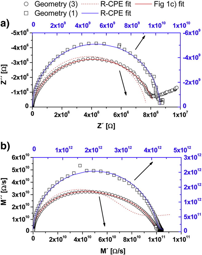
Impedance spectra measured on layer A (105 nm thin) with two different electrode geometries at 300 °C. Frequency range was 1 MHz to 1 Hz with 10 points per decade. Diagram (a) is a Nyquist plot, and (b) is a modulus plot of the data. Geometry (3) is an interdigital electrode (Fig. 2c) with 5 μm broad fingers having a distance of 10 μm, the effective electrode length was measured to be 14.40 cm. Geometry (1) consists of approximately 5 mm broad, 500 μm spaced stripes of 8 mm length (Fig. 2(a)). For easier comparison of the different shapes of the spectra different scales are used for Geometry (3) (black) and Geometry (1) (blue). The red lines are fitting results for Geometry (3) with an R–CPE equivalent circuit (dotted line) and the circuit in Fig. 1(c) (solid line). The solid blue line is a fit to data from Geometry (1) with a single R–CPE equivalent circuit (n ≈ 1). The arrows indicate the appropriate axis scales.
Strongly overlapping rather than well separated arcs (cf. Fig. 3(d)) can be attributed to the constant phase elements with exponents being smaller than 1. The values determined from the measurements usually varied between n = 0.7 and 0.8 for the grain boundary capacitance, while for the substrate stray capacitance n was very close to 1. To calculate capacitances from the constant phase element of the grain boundaries
| (6) |
was used (see Ref. [39]). These observations already indicate a successful separation of grain and grain boundary effects. However, for further verification several different interdigital electrode geometries were investigated on layer A (105 nm thick). The results of the measured capacitances and the numerically calculated substrate capacitances are summarized in Table 2. For comparison, macroscopic measurements on a YSZ polycrystal and a YSZ single crystal are also included. The resulting conductivities are plotted in an Arrhenius diagram in Fig. 8. The appropriateness of the resulting geometry dependence of the fit elements will be discussed in the following.
Table 2.
Capacitance values averaged over the temperature range from 200 °C to 400 °C, resistance values obtained at 300 °C and activation energies, all determined on layer A (105 nm thick) for different electrode geometries. For comparison, calculated substrate capacitances and activation energies of poly- and single crystalline YSZ are shown. Capacitances and resistances are normalized to the electrode length. Measured stray capacitances are averaged over values of Q with n > 0.98 for the constant phase element in Fig. 1(c).
| Electrode geometry |
CGB [pF/m] | CStray [pF/m] | CSubstrate calculated [pF/m] | RBulk at 300 °C [MΩcm] | RGB at 300 °C [MΩcm] | Ea bulk [eV] | Ea GB [eV] | ||
|---|---|---|---|---|---|---|---|---|---|
| Distance [μm] | Width [μm] | Length [cm] | |||||||
| 10 | 5 | 14.40 | 91 ± 6 | 85 ± 7 | 69 | 34.0 ± 0.8 | 85 ± 1 | 0.99 | 1.10 |
| 10 | 10 | 12.76 | 80 ± 10 | 94 ± 9 | 88 | 42.5 ± 0.8 | 103 ± 1 | 0.98 | 1.14 |
| 25 | 5 | 10.08 | 39 ± 5 | 69 ± 6 | 51 | 75 ± 2 | 190 ± 2 | 0.95 | 1.17 |
| 25 | 10 | 9.20 | 45 ± 6 | 89 ± 5 | 64 | 52 ± 2 | 164 ± 3 | 0.97 | 1.14 |
| 500 | 5000 | 0.8 | – | 33 ± 4 | 47 | – | – | 1.12 | |
| YSZ polycrystal | – | – | – | – | – | 1.05 | 1.17 | ||
| YSZ single crystal | – | – | – | – | – | 1.11 | –- | ||
Fig. 8.

Arrhenius plot of the conductivities measured with different electrode geometries on layer A (105 nm thin). In the caption the corresponding distances (D) and widths (B) are specified in μm. The solid red (9.5% YSZ single crystal) and dotted green (8% YSZ polycrystal) lines are macroscopic bulk measurements plotted for comparison. The solid black line is the effective total conductivity of the film measured with Geometry (1).
Calculated and measured values for the stray capacitances are in acceptable agreement for all the geometries and follow the predicted trend, even though the simulated values are somewhat lower than the measured ones. This might be explained by two factors: firstly, the calculated values are based on a two dimensional simulation, which neglects additional capacitive contributions of the interdigital design, for example caused by the current collectors. Secondly, the capacitive contribution of the surrounding air was not included in the simulation either. A combination of these effects can explain an underestimation of about 15%, which is close to the measured deviation. Hence, we conclude that the simulation is very useful in predicting electrode configurations for which a separation becomes feasible and that the fit parameter CStray is indeed the stray capacitance.
According to Eq. (3) the grain boundary capacitance should only depend on the spacing of the electrodes, when being normalized to the electrode length. When comparing the grain boundary capacitances in Table 2, the averaged measured ratio for 25 μm and 10 μm spaced electrodes is about 2. This shows the predicted trend of the electrode distance even though that the value of 2.5 expected from Eq. (3) is not exactly met. Partly this might be due to the simplified electrode geometry used in the modelling and Eq. (3) (e.g. neglecting displacement current beneath the electrodes, see Refs. [33], [34]). Also neglecting CBulk in the equivalent circuit (see above) may play a role. The capacitance of the contacting needles and the setup (CWiring) was measured to be 25 fF, which is at least two orders of magnitude smaller than the grain boundary capacitance; it should thus be of no importance in our case.
The grain boundary thickness was calculated from the measured values of CGB in Table 2 with Eq. (3) and an averaged value of dgb = 1.0 nm results for the grain size dg = 19 nm. This value for the grain boundary thickness is in the range of the structural width of the interface and significantly smaller than values obtained on macroscopic samples and also on thicker layers: in Ref. [5] dgb = 5.4 nm for dg ≥ 232 nm is reported. For polycrystalline samples the values are in the same range (dgb = 5 nm independent of dg [25]; dgb = 5.4 nm for dg > 350 nm [26]). Using the nanograin composite model dgb = 4.2 nm for dg = 26 nm is reported in Ref. [36]. However, in all these cases the grains are of more or less "isotropic" shape and randomly oriented, while in the present case highly textured columnar grains in PLD layers are studied. While inaccuracies in the measurements and the simplified model used for fitting the impedance data might contribute to the small value calculated in the present study, we would also not exclude that a grain boundary width of about 1 nm is indeed a true property of the layer. However, more experimental data is needed to confirm or reject this hypothesis.
The measured (fitted) grain and grain boundary resistances at 300 °C as well as the corresponding activation energies are given in Table 2. Grain boundary and bulk resistances at the same temperatures and corrected to the electrode length are indeed almost indirectly proportional to the electrode distance. A resistance increase by a factor of approximately 1.9 for the grain boundaries and of 1.7 for the bulk is found. Deviations from the value of 2.5 (ratio of the electrode distance) might originate from slight temperature variations of a few degrees on the sample surface; also in this case the simplified model neglecting CBulk may have an effect, as well as the idealized treatment of the interdigital electrodes [33], [34].
The activation energy for ion conduction in the grain bulk of our film (ca. 0.98 eV) is in good agreement with the value of our macroscopic polycrystalline material of 1.05 eV or 1.08 eV as given in Ref. [5]. The absolute value of the bulk conductivity, calculated from RBulk and the geometrical parameters h, D, L according to
| (7) |
correlates quite well with macroscopic values of poly- or single crystalline samples (Fig. 8). This means that the lower overall conductivity of our YSZ films (indicated in Fig. 8 by the effective conductivities of Geometry (2) with D = 500 μm and B = 5000 μm) is indeed only due to blocking grain boundaries. Bulk properties are hardly changed even in a film of 100 nm thickness and a grain size of approximately 20 nm. The deviations obtained at higher temperatures are explained by the fact that the high relaxation frequencies of the bulk make the fit data less accurate.
Transport through the grain boundaries with an activation energy of 1.14 eV is in accordance with that of the macroscopic reference of 1.17 eV and the value in Ref. [5] of about 1.15 eV. The associated conductivity (Fig. 8) was calculated according to
| (8) |
with dg = 19 nm and dgb = 1.0 nm. As in Eqs. (2), (3), (7) this relation neglects current beneath the electrodes but proves to be a good approximation for all films considered here (h ≪ D) [33], [34]. The grain boundary conductivity is about two orders of magnitude smaller than the corresponding bulk values, which is again the same ratio as in Ref. [5]. All together, the geometry dependence of all fit parameters, the absolute values of grain boundary thickness and bulk conductivity and the reasonable activation energies indicate that indeed bulk and grain boundaries were successfully separated in a 100 nm thick YSZ layer of 20 nm grain size.
4.2.2. Effect of film thickness and crystallinity
The following section illustrates the influence of grain size and film thickness on the capacitances and resistances in our system. The samples B (18 nm thick) and C (32 nm thick) were quartered and three of the equally sized pieces were annealed for 1, 3, and 5 h at 1000 °C. Subsequently, impedance spectra were recorded for each of these pieces. A geometry with 5 μm broad and 25 μm spaced interdigital electrodes was used in these investigations. As the measurements on the as-prepared (non-annealed) samples did not yield meaningful results in terms of grain and grain boundary separation, they are not included in the discussion. In Fig. 9 the spectra of layer C, annealed for 1 and 5 h, are compared and the corresponding fit functions are plotted. Again a good approximation by the reduced equivalent circuit in Fig. 1(c) is possible and even a slight change in the overall shape of the spectra is visible.
Fig. 9.

Modulus plot of impedance spectra recorded on layer C (32 nm thin) at 300 °C. Please note the different scalings used for the spectra in order to allow easier comparison. The open circles (black axis scale) correspond to 1 h annealing time at 1000 °C, the open squares (blue axis scale) to 5 h at 1000 °C. The solid red and blue lines represent the corresponding fit functions obtained by using the equivalent circuit depicted in Fig. 1(c). In both cases the electrode geometry consisted of 25 μm spaced 5 μm broad electrodes. The arrows indicate the appropriate axis scales.
The change of the grain boundary capacitances with annealing time is illustrated in Fig. 10(a). The capacitance increases with annealing time, probably due to an increase in grain size dg caused by crystallization (see Eq. (3)). Since the increase of the grain boundary capacitance is about a factor of 2 for layer C, the grain size should also have doubled provided that the grain boundary thickness remains constant. However, such an increase in grain size could not be verified by AFM. Thus, also chemical or crystallographic changes at the grain boundaries decreasing the electrical grain boundary width dgb cannot be excluded. The ratio of the grain boundary capacitances for different film thickness but identical annealing times amounts to Cgb(C)/Cgb(B) = 1.4 (1 h) and 1.6 for (5 h), and hence approaches the ratio of the layer thicknesses (1.8). This is a very reasonable result since exactly 1.8 can only be expected, if after annealing both layers had equal dg/dgb ratio.
Fig. 10.

(a) Change of grain boundary capacitance and (b) substrate stray capacitance with annealing time for layer B and C at 1000 °C. The solid lines in (a) are linear fits of the data. The stray capacitances plotted in (b) are not calculated by Eq. (6), but values of Q were taken for n > 0.98. The values and the error bars in (a) and (b) are calculated from several spectra recorded at temperatures from 250 to 550 °C. The open symbols in (a) and (b) at 0 h annealing indicate that meaningful fit results could not be obtained in that case.
The normalized stray capacitance is plotted in Fig. 10(b) and does not change with annealing time. This is in agreement with our model and Eq. (4), where the stray capacitance only depends on the electrode geometry, which is the same for both layers. It thus further supports the correct interpretation of the elements in the reduced equivalent circuit.
Comparing the resistances of the different annealing states of layers B and C is more complicated. Firstly, the layers may have crystallized to a different degree after the same annealing time and, secondly, grain size and thus also grain boundary width is unknown. The normalized resistances obtained after 1 and 5 h of annealing at 1000 °C for grain bulk and grain boundaries of layers B and C are listed in Table 3. The ratio of the bulk resistances, RBulk(C)/RBulk(B), for the shorter annealing time is about 0.25, and therefore smaller than the ratio of the inverse layer thickness of about 0.56. However, for longer annealed samples, a ratio of 0.52 is measured, which suggests that then both layers have crystallized to a comparable degree and exhibit the same bulk conductivity. This is in very good agreement with the XRD analysis, which resulted in the same lattice parameter for both annealed samples. The ratio of normalized grain boundary resistances changes from 0.5 to 0.25 with increasing annealing time, which reflects an opposite trend compared to the bulk resistance. This means that the grain boundary resistance of the thinner layer is indeed larger, but does not simply scale with the inverse thickness. Rather, also the grain boundary conductivity might differ for annealed films of different thickness. Grain size and grain boundary thickness variations are less probable, because the capacitance ratio is almost correct.
Table 3.
Stray and grain boundary capacitances as well as activation energies for transport through grain bulk and grain boundaries (GB) and the corresponding resistances at 300 °C measured on layers B and C with different annealing times. Capacitances and resistances are normalized to the electrode length. Measured stray capacitances are averaged over values of Q with n > 0.98 for the constant phase element in Fig. 1(c).
| Sample | Annealing time at 1000 °C [h] | CGB [pF/m] | CStray [pF/m] | RBulk at 300 °C [GΩcm] | RGB at 300 °C [GΩcm] | Ea bulk [eV] | Ea GB [eV] |
|---|---|---|---|---|---|---|---|
| B (18 nm thickness) | 0 | 40 ± 20 | 55 ± 6 | 7.3 ± 0.1 | 7.9 ± 0.2 | 0.82 | 0.890 |
| 1 | 16 ± 4 | 54 ± 3 | 1.95 ± 0.05 | 4.64 ± 0.05 | 0.99 | 1.12 | |
| 3 | 20 ± 10 | 54 ± 6 | 1.66 ± 0.05 | 5.75 ± 0.05 | 0.88 | 1.18 | |
| 5 | 23 ± 3 | 66 ± 6 | 0.69 ± 0.04 | 4.01 ± 0.06 | 0.87 | 1.10 | |
| C (32 nm thickness) | 0 | 14 ± 6 | 81 ± 10 | 0.44 ± 0.05 | 5.11 ± 0.05 | 0.85 | 1.38 |
| 1 | 22 ± 6 | 57 ± 6 | 0.53 ± 0.03 | 2.17 ± 0.03 | 0.88 | 1.21 | |
| 3 | 30 ± 10 | 52 ± 6 | 0.49 ± 0.02 | 1.46 ± 0.02 | 0.93 | 1.11 | |
| 5 | 38 ± 9 | 63 ± 4 | 0.36 ± 0.01 | 1.18 ± 0.01 | 0.91 | 1.13 |
The Arrhenius plot in Fig. 11 shows the bulk conductivities calculated from the fit results. The results after 5 h annealing time are very close to the bulk conductivities of macroscopic samples again supporting the conclusion that the separation into resistive contributions works and that after 5 h annealing at 1000 °C films are sufficiently crystalline. Reasons for the deviation of the film conductivities from macroscopic samples at higher temperatures have already been mentioned above. Bulk as well as grain boundary activation energies are summarized in Table 3 and again reflect the trend well known from macroscopic polycrystals [29]: the grain boundary activation energy of about 1.1–1.2 eV is larger than that of the bulk (ca. 0.9 eV). All together, also the measurements on films of different thickness and annealing time confirm that a separation into grain and grain boundary impedance contributions can be successful with optimized electrodes even on films as thin as ca. 18 nm.
Fig. 11.
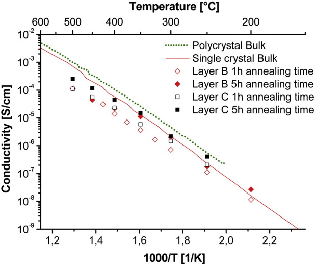
Arrhenius plot of the grain bulk conductivities measured on layers B (18 nm thickness) and C (32 nm) with different annealing times at 1000 °C. Bulk conductivities of macroscopic samples are plotted for comparison (9.5% YSZ single crystal and 8% YSZ polycrystal).
5. Conclusions
Modelling with finite element calculations, analytical considerations and simulation of impedance spectra illustrate that measurements using the generally employed electrode geometries usually result in high stray capacitances, which hinder separation of grain and grain boundary effects. Such considerations also suggest that an optimized electrode geometry may enable separation of grain and grain boundary contributions to electrical impedance spectra even for very thin ion conducting layers. The optimization strategy consists of preparing long, thin, and closely spaced stripe electrodes, which strongly reduce the masking effect of the substrate stray capacitance. This can most easily be realized when arranging the electrodes interdigital. Even though in Nyquist plots separation may not be seen, modulus plots show distinct grain and grain boundary contributions.
In order to experimentally test the suggested approach, YSZ thin films were deposited on sapphire single crystals using pulsed-laser deposition and were characterized by impedance spectroscopy. The drastic effect of different electrode geometries on the stray capacitance, and thus on the shape of the spectrum (particularly in the modulus plot), was demonstrated on a fully crystalline layer. The influence of layer thickness and grain size was studied on films annealed for different times. All recorded spectra could be fitted by the suggested equivalent circuit (Fig. 1(c)) and the resulting bulk conductivities correlate well with bulk values obtained on macroscopic reference samples. The grain boundary capacitance showed the expected dependency on electrode geometry and film thickness and yielded a grain boundary thickness of 1 nm. The stray capacitance did only depend on electrode geometry and was neither influenced by the annealing time nor by the YSZ film thickness. Consequently, the properties of all fit elements support the initial considerations.
Hence, we conclude that a separation of grain and grain boundary effects can be achieved in YSZ layers as thin as 20 nm by means of impedance spectroscopy and that this method is a promising tool for further studies also on other ion conducting thin films.
Acknowledgement
The authors gratefully acknowledge Erich Halwax for XRD measurements, Stefan Krivec for DHM measurements, and the financial support of the Austrian Science Fund (FWF) project "Ion transport in thin oxide films" P19348-N17.
References
- 1.Muecke U.P., Beckel D., Bernard A., Bieberle-Hutter A., Graf S., Infortuna A., Muller P., Rupp J.L.M., Schneider J., Gauckler L.J. Adv. Funct. Mater. 2008;18(20):3158. [Google Scholar]
- 2.Infortuna A., Harvey A.S., Gauckler L.J. Adv. Funct. Mater. 2008;18(1):127. [Google Scholar]
- 3.Heiroth S., Lippert T., Wokaun A., Dobeli M. Appl. Phys. Mater. 2008;93(3):639. [Google Scholar]
- 4.Joo J.H., Choi G.M. Solid State Ionics. 2006;177(11–12):1053. [Google Scholar]
- 5.Peters C., Weber A., Butz B., Gerthsen D., Ivers-Tiffee E. J. Am. Ceram. Soc. 2009;92(9):2017. [Google Scholar]
- 6.Kosacki I., Rouleau C.M., Becher P.F., Bentley J., Lowndes D.H. Solid State Ionics. 2005;176(13–14):1319. [Google Scholar]
- 7.Gmucova K., Hartmanova M., Kundracik F. Ceram. Int. 2006;32(2):105. [Google Scholar]
- 8.Wang H.B., Xia C.R., Meng G.Y., Peng D.K. Mater. Lett. 2000;44(1):23. [Google Scholar]
- 9.He X.D., Meng B., Sun Y., Liu B.C., Li M.W. Appl. Surf. Sci. 2008;254(22):7159. [Google Scholar]
- 10.Fergus J.W. J. Power Sources. 2006;162(1):30. [Google Scholar]
- 11.Chiodelli G., Malavasi L., Massarotti V., Mustarelli P., Quartarone E. Solid State Ionics. 2005;176(17–18):1505. [Google Scholar]
- 12.Chen L., Chen C.L., Chen X., Donner W., Liu S.W., Lin Y., Huang D.X., Jacobson A.J. Appl. Phys. Lett. 2003;83(23):4737. [Google Scholar]
- 13.Suzuki T., Kosacki I., Anderson H.U. Solid State Ionics. 2002;151(1–4):111. [Google Scholar]
- 14.Kosacki I., Suzuki T., Petrovsky V., Anderson H.U. Solid State Ionics. 2000;136–137:1225. [Google Scholar]
- 15.Joo J.H., Choi G.M. Solid State Ionics. 2008;179(21–26):1209. [Google Scholar]
- 16.Joo J.H., Choi G.M. J. Eur. Ceram. Soc. 2007;27(13–15):4273. [Google Scholar]
- 17.Pryds N., Toftmann B., Bilde-Sorensen J.B., Schou J., Linderoth S. Appl. Surf. Sci. 2006;252(13):4882. [Google Scholar]
- 18.Sillassen M., Eklund P., Sridharan M., Pryds N., Bonanos N., Bottiger J. J. Appl. Phys. 2009;105(10) [Google Scholar]
- 19.Chun S.Y., Mizutani N. Appl. Surf. Sci. 2001;171(1–2):82. [Google Scholar]
- 20.Schichtel N., Korte C., Hesse D., Janek J. Phys. Chem. Chem. Phys. 2009;11(17):3043. doi: 10.1039/b900148d. [DOI] [PubMed] [Google Scholar]
- 21.Cheikh A., Madani A., Touati A., Boussetta H., Monty C. J. Eur. Ceram. Soc. 2001;21(10–11):1837. [Google Scholar]
- 22.Brossmann U., Knoner G., Schaefer H.E., Wurschum R. Rev. Adv. Mater. Sci. 2004;6(1):7. [Google Scholar]
- 23.Knoner G., Reimann K., Rower R., Sodervall U., Schaefer H.E. P. Natl Acad. Sci. USA. 2003;100(7):3870. doi: 10.1073/pnas.0730783100. [DOI] [PMC free article] [PubMed] [Google Scholar]
- 24.De Souza R.A., Pietrowski M.J., Anselmi-Tamburini U., Kim S., Munir Z.A., Martin M. Phys. Chem. Chem. Phys. 2008;10(15):2067. doi: 10.1039/b719363g. [DOI] [PubMed] [Google Scholar]
- 25.Guo X., Zhang Z.L. Acta Mater. 2003;51(9):2539. [Google Scholar]
- 26.Verkerk M.J., Middelhuis B.J., Burggraaf A.J. Solid State Ionics. 1982;6(2):159. [Google Scholar]
- 27.Kushima A., Yildiz B. J. Mater. Chem. 2010;20(23):4809. [Google Scholar]
- 28.Ning X.J., Li C.X., Li C.J., Yang G.J. Mat. Sci. Eng. Struct. 2006;428(1–2):98. [Google Scholar]
- 29.Guo X., Waser R. Prog. Mater. Sci. 2006;51(2):151. [Google Scholar]
- 30.Bauerle J.E. J. Phys. Chem. Solids. 1969;30(12):2657. [Google Scholar]
- 31.Maier J. Ber. Bunsen. Phys. Chem. 1986;90(1):26. [Google Scholar]
- 32.Fleig J., Maier J. J. Eur. Ceram. Soc. 1999;19(6–7):693. [Google Scholar]
- 33.Kidner N.J., Homrighaus Z.J., Mason T.O., Garboczi E.J. Thin Solid Films. 2006;496(2):539. [Google Scholar]
- 34.Kidner N.J., Meier A., Homrighaus Z.J., Wessels B.W., Mason T.O., Garboczi E.J. Thin Solid Films. 2007;515(11):4588. [Google Scholar]
- 35.Hendriks M.G.H.M., ten Elshof J.E., Bouwmeester H.J.M., Verweij H. Solid State Ionics. 2002;146(3–4):211. [Google Scholar]
- 36.Perry N.H., Kim S., Mason T.O. J. Mater. Sci. 2008;43(14):4684. [Google Scholar]
- 37.Kosacki I. Nato Sci. Ser. Ii Math. 2005;202:395. [Google Scholar]
- 38.Jang J.W., Kim H.K., Lee D.Y. Mater. Lett. 2004;58(7–8):1160. [Google Scholar]
- 39.Fleig J. Solid State Ionics. 2002;150(1–2):181. [Google Scholar]