Abstract
Biologically sensitive field-effect transistors (BioFETs) are one of the most abundant classes of electronic sensors for biomolecular detection. Most of the time these sensors are realized as classical ion-sensitive field-effect transistors (ISFETs) having non-metallized gate dielectrics facing an electrolyte solution. In ISFETs, a semiconductor material is used as the active transducer element covered by a gate dielectric layer which is electronically sensitive to the (bio-)chemical changes that occur on its surface. This review will provide a brief overview of the history of ISFET biosensors with general operation concepts and sensing mechanisms. We also discuss silicon nanowire-based ISFETs (SiNW FETs) as the modern nanoscale version of classical ISFETs, as well as strategies to functionalize them with biologically sensitive layers. We include in our discussion other ISFET types based on nanomaterials such as carbon nanotubes, metal oxides and so on. The latest examples of highly sensitive label-free detection of deoxyribonucleic acid (DNA) molecules using SiNW FETs and single-cell recordings for drug screening and other applications of ISFETs will be highlighted. Finally, we suggest new device platforms and newly developed, miniaturized read-out tools with multichannel potentiometric and impedimetric measurement capabilities for future biomedical applications.
Keywords: field-effect-based biosensors, field-effect transistors, silicon nanowire sensors
Introduction
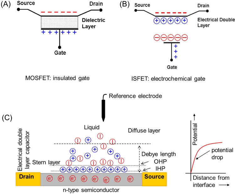
Field-effect transistor (FET) biosensors are typically fabricated using silicon or metal oxides. Since the inception of silicon technology it became the primary choice of semiconductor material in biosensing because of its mature development in the computer industry [1]. Since 1971, silicon-based FETs have been deployed in chemosensory applications such as pH-sensing in electrolyte solutions [2]. A typical semiconductor possesses a net surface charge when in contact with an electrolyte solution due to protonation and de-protonation of surface functional groups at the solid/liquid interface, which has a direct effect on the effective gate voltage and hence on the charge-carrier flow through the channel. An FET device can therefore translate (bio-)chemical binding events or ionic concentration changes on its surface into a measureable electronic signal related to the surface properties of the gate input [3]. The underlying principle of the transduction mechanism in ISEFTs is shown in Figure 1.
Figure 1. Schematic representation of the operation principle of MOSFETs and ISFETs.
(A) The three-electrode configuration in a MOSFET with a dielectric insulator material sandwiched between the channel and gate electrodes. (B) In transistors made from metal oxides or in graphene-based FETs the EDL can replace the high dielectric insulator material of the standard ISFET configuration. (C) Microscopic representation of the formation of the EDL and electrical double layer capacitance on a solid–liquid interface of an ISFET. IHP, inner Helmholtz plane; OHP, outer Helmholtz plane.
When applying a bias voltage, charge-carriers flow from the source to the drain electrode forming the drain-source current. The flow of charge-carriers in the FET channel is controlled by applying an electrical field from a third electrode called a gate. Applying a positive or negative voltage at the gate can increase or decrease the number of charge-carriers in the channel, thereby switching the FET on or off. This is realized by the gate-source voltage, which generates an electrical field in the transistor channel and hence influences the channel's conductance. The mechanism of exerting an electrical field in the conductive channel varies in different FET types. The gating efficiency is related to the intrinsic properties of the material used in the architecture determining the device's properties such as conductivity, on/off ratio or cut-off frequency. In metal-oxide semiconductor field-effect transistors (MOSFETs) a material with a high dielectric constant (k) is sandwiched between the channel and the gate electrode and serves as aplanar capacitor. This configuration, consisting of an insulated gate transistor and controlling the channel by purely capacitive coupling, is the standard design used in today's integrated circuits of the computer industry.
Depending on the method of applying the gate voltage and on the design and material of the gate and channel region, insulated gate FETs can be categorized into different types such as junction field-effect transistors (JFET), ion-sensitive field-effect transistors (ISFETs), metal-semiconductor field-effect transistors (MESFETs), etc. Although the basic principle of controlling the channel conductance is similar in all FETs, the mechanism of the gate coupling can differ significantly. For sake of brevity, in this review we will focus our discussion only on ISFETs [2].
In ISFETs, the insulator-gate mechanism responsible for the operation of MOSFETs is replaced by an electrochemical gating effect [2]. There are two main differences in this insulator-gate mechanism. In the classical form of ISFETs, a dielectric insulator is present (e.g. SiO2 or other oxide dielectrics). In this case, the capacitive coupling is dominated by the gate dielectrics itself and the capacitance of the electrical double layer (EDL) can be neglected. If the gate insulator is omitted, as is the case for many carbon and metal-oxide FETs, the insulation of the gate is defined by the creation and composition of the EDL, which arises from the redistribution of the ions in the solution in the vicinity of the surface and exerts a capacitance on the channel called an electrical double layer capacitance (EDLC). There are also intermediate forms possible [4], where only a thin and non-perfect insulator is left (such as natural silicon oxide), which is then characterized by high gate leakage currents. In general, the EDLC can be controlled by applying a potential in the liquid (Figure 1C) [5,6]. In electrochemically gated ISFETs, the EDLC can be calculated by using the capacitance model as for MOSFETs. The thickness and other electrostatic properties of the EDL are influenced by the ionic composition of the solution and by the voltage applied to the structure.
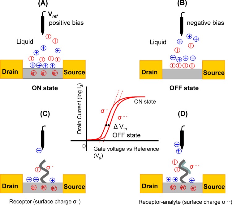
The polarity of the EDL can be changed by switching the bias voltage in the solution and therefore varying the number of charge-carriers in the channel bringing the ISFET into the ON or OFF state (Figures 2A and 2B). Generally, an electrochemical reference electrode (most of the time a liquid-gated Ag/AgCl electrode) is used to apply and precisely control this bias voltage in solutions. The functionalization of charged biomolecules (receptors) on the surface and selective binding of analyte molecules will lead to alterations of the surface charge and therefore a net change of the effective gate voltage is needed to switch the ISFET into the ON or OFF state (Figures 2C and 2D). For further details on the operation of ISFETs, readers are encouraged to consult the book by Besselink and Bergveld on ISFET-based affinity biosensors [2].
Figure 2. Principle of the operation of an ISFET- and FET-based transducer.
(A and B) Applying positive and negative bias at the Ag/AgCl reference electrode change the polarity of the electrical double layer. (C and D) Change in the net charge-carrier density on an ISFET surface modified with a receptor biomolecule before and after binding with an analyte molecule. The change in the net surface charge shifts the field-effect curve as shown in the graph in the centre.
Biologically sensitive field-effect transistors (BioFETs)
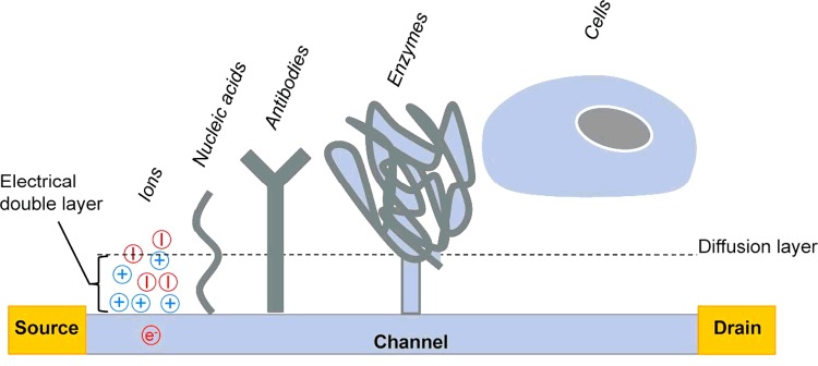
BioFETs are ISFETs which are sensitive towards a selection of biomolecules or chemical analytes due to the introduction of a bio-recognition layer at their surface. This layer is chemically or electrostatically bound to the transducer surface. The choice of this bio-recognition layer is critical to the biosensor performance and should provide specific interaction with target molecules, minimize non-specific binding and, in some cases, facilitate a charge transfer. The nature of the recognition layers varies depending on the application (Figure 3).
Figure 3. Schematic representation of a biologically sensitive ISFET and different types of analytes with variable sizes in relation to the thickness of the EDL (analyte size is not to scale).
Only DNA molecules present charges inside the EDL, whereas only fractions of the much larger antibody and enzyme molecules directly affect the EDL (only in the case of diluted buffer concentrations). In the case of cells, the cellular membrane is clearly outside this range, since typical average distances between the cellular membrane and the surface are in the range 50–100 nm.
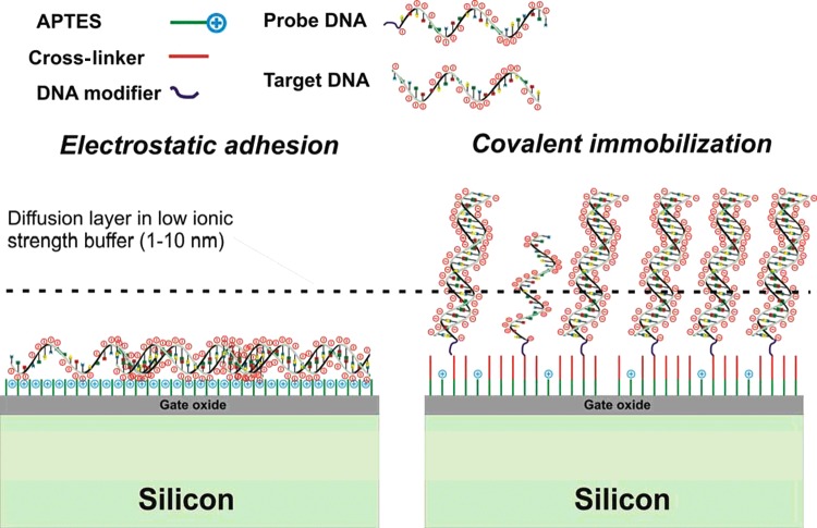
The inherent surface charge-sensitivity of ISFETs can also be exploited for the direct label-free detection of charged molecules such as DNA, RNA and peptides. The detection works by the ‘lock and key’ model for receptor–analyte interactions. These specific molecular interactions on the transducer surfaces affect the charge-transport characteristics of the FET. In BioFETs for DNA detection, single-stranded capture DNAs are immobilized using electrostatic or covalent functionalization methods (Figure 4) [7,8]. The determination of methods to assemble a highly defined and uniform supramolecular architecture of the probe biomolecules has always been of considerable interest. Covalent functionalization methods for probes using silanes and other methods such as ED–NHS coupling allow robust anchoring, efficient charge transfer and help retain the bioactivity of the receptor molecules [9,10].
Figure 4. Different strategies for the immobilization of probe DNA.
On the left, the DNA molecules are attached to the aminosilane layer by electrostatic immobilization. This usually leads to high FET signal amplitudes for the immobilization process because the oligonucleotides are very closely attached to the gate oxide. The hybridization efficiency, however, is not very high in these experiments. On the right, the probe single-stranded DNA (ssDNA) is covalently attached utilizing a cross-linker in combination with end-functionalized ssDNA. Generally, the double-stranded molecules are stiffer and longer compared with the unoccupied ssDNA molecules. For alternative silane layers other cross-linkers and covalent linking strategies are used.
For the electrical detection of biomolecules in solutions using ISFETs, different read-out strategies have been proposed. For small and charged biomolecules in low ionic strength solutions, a simple potentiometric read-out usually serves the purpose. The detection of biomolecules such as proteins, however, was reported to be very difficult and most of the time unreliable. In this context, the direct current (DC) as well as the alternating current (AC) read-out of the FETs has been elaborated and the influence of a biomembrane attached to the transistor gate structure has been described [11]. For the detection of slightly bigger molecules extending beyond the EDL in physiological solutions, a more sophisticated impedimetric read-out (AC measurement) was introduced, where the transfer function for BioFETs provides more accurate information [12–14]. In very recent work, a theoretical foundation has also been provided and AC recordings at very high frequency (>10 MHz) with a capacitive coupling approach has shown superior performance compared with DC recording or AC recording at lower frequency levels (about 10 kHz) [13].
Cell-based BioFETs
The ability of BioFETs to address living cells and read biological information has been one of the major applications that have the potential to gain insight into many different areas such as drug screening, interactions of biochemical compounds with living systems, their effect and classification. BioFETs are also deployed for studying neuronal networks and other cellular pathways. Coupling different kinds of cells on to electronic sensor platforms has led to a number of cell-based biosensor concepts [15]. Among other applications, BioFETs have been on the forefront for recording extracellular signals from electrogenic cells in vitro.
The first FETs for the recording of electrical cell signals were developed by the group of Bergveld [16]. Later, several groups developed FETs for the recording of neurons and cardiac cells [17,18]. Most of these sensor chips were operated as potentiometric ISFETs at higher sampling rates (>3 kHz) to read the full spectral information of cellular action potentials [19–21]. The most sophisticated platforms, with ultrahigh integration density and high sampling rates per channel, were realized over the last decade in industrial complementary metal-oxide-semiconductor (CMOS) processes and were offered commercially for interfacing with neuronal cultures [22–24].
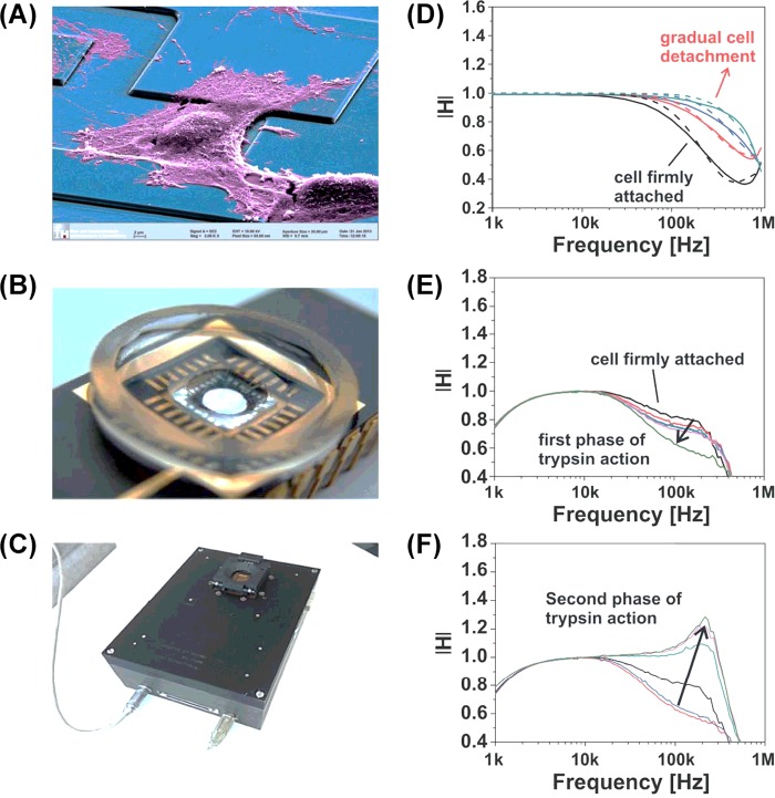
Ingebrandt et al. [12] used a differential AC read-out method for FET microarrays to detect DNA, which was based on the biomembrane formed on top of the gate oxide of an ISFET. This technique was described earlier, but was applied to test the reliability of the device's encapsulation material [25] or to detect the binding of biomolecules and/or changes in the properties of biological membranes attached to the gate structure of the FETs [26]. The same method has been extended and optimized to record the adhesion status of cellular membranes or individual cells attached at the gate of ISFETs [27,28]. An example of such a BioFET used for single cell–substrate adhesion tests is shown in Figure 5. Using these ISFETs, a novel technique for the impedimetric sensing of cellular adhesion was introduced, which might have the potential to supplement the well-known electrical cell–substrate impedance sensing (ECIS) in cell culture assays [29–31]. In other examples, three histologically different cell lines were cultivated in fluidic chambers on top of the FET devices and subjected to a microscopic analysis of gate coverage and cell adhesion using a transistor-transfer function (TTF) technique comparable with the ECIS methods. The frequency spectra depend on the morphologies of the cells and cell-related parameters [29]. Such cell-based assays could be performed using the new BioFETs designs incorporated into a pharmacological platform for studying the effects of chemical and therapeutic compounds on a variety of cells from different histological backgrounds [30]. Similarly, BioFETs were used to determine the interactions between cytotoxic T-lymphocytes and their target cells while circumventing the conventional immunofluorescence imaging methods, which are tedious and time-consuming [32]. High-density FET-arrays could potentially be further deployed to study intercellular interactions such as neuronal networks [33].
Figure 5. Monitoring of the influence of cell-related parameters at a single-cell level using impedance spectra measured with silicon-based BioFETs.
(A) A human embryonic kidney (HEK)-293 cell sitting on top of the BioFETs. (B and C) The cell-culture chamber on top of the silicon chip and the miniaturized measurement platform. (D–F) The transfer function spectra after cells were treated with trypsin while following the cell-detachment process over time [29].
Nanoscale BioFETs
With the introduction of nanomaterials and scalable nanostructuring methods, nanoscale ISFETs have taken centre stage in the development of novel biosensor platforms. Miniaturization, high sensitivity and unique material properties at the nanoscale have the potential to yield highly integrated versatile sensor platforms with multiplex and multiple read-out possibilities, crucial for the development of next-generation point-of-care (PoC) systems. In this quest, the last few decades have marked the discovery of nanomaterials used for the realization of high-performance nanoscale BioFETs. The rediscovery of carbon nanotubes (CNTs) in 1991 by Sumo Injima [34] as one-dimensional structures with unique electrical characteristics and a high surface-to-volume ratio perhaps brought the most important turnaround for the realization of high-sensitivity nanoelectronic devices [35]. CNTs were subsequently deployed for biomolecular sensing. After the discovery and implementation of CNTs into biosensor platforms, researchers began to use silicon nanowires (SiNWs) grown by chemical vapor deposition (CVD) and apply them in bottom-up approaches as transducer elements in modern, nanoscale biosensors. A large number of articles were published in this field and interested readers should consult published studies performed in the laboratory of C. Lieber [36,37]. Parallel to this, researchers applied standard silicon technology to realize top-down processed SiNW platforms [38–41]. Techniques such as e-beam lithography and etching processes for prototyping new device architectures with controllable electronic properties of SiNWs (unlike CNTs) emerged as a reliable platform for biomedical signalling purposes [42]. The use of SiNW- and CNT-based BioFETs for the label-free detection of biomolecules was catapulted into a myriad of applications such as detection of glucose, enzymes, proteins and hormones, and many of these research groups picked up ideas that had been elaborated upon in the 1980s and early 1990s with microsized ISFETs.
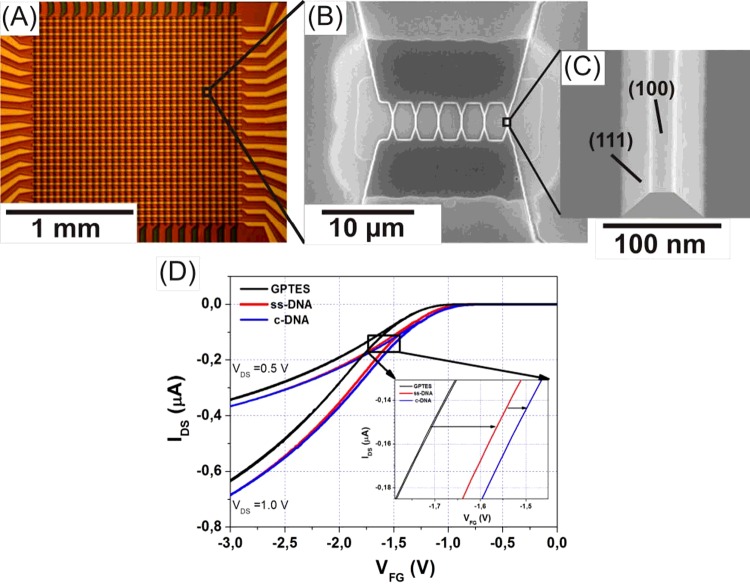
In the race towards the realization of high-performance BioFETs, DNA biomarkers have always been at the forefront [7,37,40]. Ingebrandt et al. [42] presented a novel approach for a large-scale SiNW array fabrication where nanoimprint lithography was combined with standard CMOS processing on 10 cm silicon-on-insulator (SOI) wafers. Such SiNW FETs with superior sensor characteristics implemented in a differential read-out demonstrated the reliable detection of biomolecules (Figure 6) [42].
Figure 6. Detection of immobilized DNA on SiNW FETs.
(A–C) A high-density SiNW FET chip with a detailed structural view taken by scanning electron microscopy. (D) Transfer characteristics before (left curve) and after DNA immobilization (middle curve), and after hybridization (right curve). DNA was site-selectively immobilized on some channels of the array using a micro-spotter. Depending on the grafting density of the molecules and on the hybridization efficiency typical shifts of 10–200 mV are recorded with the silicon nanowire devices. This is much larger than typical signals recorded with ISFETs [42].
There is a currently a strong drive in this field, but most groups are using DC read-outs for the assays. As discussed above, this transducer principle is usually reliable in DNA assays with detection in diluted buffer solutions so that the charged-based sensing can be exploited. For the detection of larger molecules, however, the detection schemes generally become unstable and more difficult to control.
Future trends and novel transducer principles for BioFETs
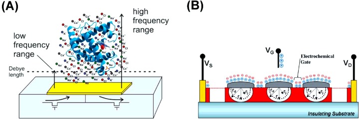
In this section, new device architectures and new transducer principles to deal with the above-mentioned fundamental limitations of the sensor platforms are discussed. For example, one of the major disadvantages of traditional charge-based molecular detection approaches that work at low frequencies is that they are only sensitive to the biomolecules that are a short distance (∼1 nm) away. This is related to the Debye screening of electronic charges caused by counter-ions in the buffer solutions. In contrast with this, new platforms such as CMOS nanocapacitors as shown in Figure 7(A) can operate at much higher frequencies (up to 50 MHz) and reach further into the solution [13]. Similarly, such screening and Debye length issues can also be tackled by changing the surface architecture of the sensor devices such as nanowire-nanoparticle hybrids forming so-called ion-sensitive metal-semiconductor field-effect transistors (ISMESFETs) with enhanced performance as demonstrated earlier (Figure 7B) [43].
Figure 7. CMOS nanocapacitors (A) and ISMESFETs (B) are new concepts in measurement methods and device architectures.
The massive parallel sequence analysis of biomolecules such as nucleic acids and their use in genetics, medicine and drug discovery has led to a broad interest in PoC diagnostics. In this regard, miniaturized amplifier systems are required that are able to integrate nanoscale devices and provide low-noise and stable electrical signals from the sensor. In our recent projects, we fabricated and applied such a PoC system demonstrator for different biomedical applications. Two independent frequency-selective amplifiers were included for simultaneous DC and AC read-outs, which enable a total of 16 parallel channels providing an alternative operation of one 16-channel or two eight-channel SiNW chips. The transfer function scan is carried out by feeding a sinusoidal test signal with 10 mV amplitude and varying the frequency to the reference electrode from 1 Hz to 100 kHz. Test signals of exact amplitude, frequency and phase are provided by a direct-digital-synthesis device. A frequency-selective amplification is confirmed via a frequency multiplier device, which is built in to a capacitive decoupled amplification cascade.
The resulting recordings in AC mode were explained using a behavioural Personal Simulation Program with Integrated Circuit Emphasis (PSPICE) model for SiNW FET biosensors suitable to simulate frequency domain measurements. The operational model was divided into two parts: first an electrochemical part representing the liquid/solid interface at the gate input, and secondly a FET part, which simulates the SiNW characteristics. The model provides better understanding of frequency domain measurements with SiNW sensors, offers the possibility to optimize the SiNW design, and forms a basis to include and explain sensing events in future biomedical assays with our platform [44]. Very recently, a handheld PoC demonstrator which was able to measure four channels simultaneously was built and included a 32-bit PIC microcontroller. User-friendly software written in LabVIEW communicates with the hardware to record and display the measurement results.
Such advanced read-out systems with DC and AC measurement capabilities in combination with different nanoscale devices might have the potential to bring nanowire FET sensors closer to PoC applications in the near future [45].
Summary
Biologically sensitive field-effect transistors (BioFETs) have great potential in today's biomedical applications.
The combination between continuous development of nanofabrication technologies and the parallel evolution of read-out systems have great potential for revolutionary biosensor platforms in the near future, which will provide high-throughput tools for novel biomolecular assays faster than ever and push the limits of biosensor concepts.
The discovery of new nanomaterials such as graphene and other two-dimensional materials, as well as hybrid nanomaterial systems such as nanowire–nanoparticle hybrids may provide novel solutions to the current need for fast reliable cost-effective high-throughput PoC detection and push the limits of label-free biosensors in terms of sensitivity and dynamic ranges.
Standard biosensor platforms such as SiNW FETs are expected to add real value towards future biomedical applications and offer remarkable sensitivity to detect biomolecular binding events or metabolic reactions at the interface of living systems and electronics.
Abbreviations
- AC
alternating current
- BioFET
biologically sensitive field-effect transistor
- CMOS
complementary metal oxide semiconductor
- CNT
carbon nanotube
- DC
direct current
- ECIS
electrical cell.substrate impedance sensing
- EDL
electrical double layer
- EDLC
electrical double layer capacitance
- FET
field-effect transistor
- ISMESFET
ion-sensitive metal-semiconductor field-effect transistor
- JFET
junction field-effect transistor
- MESFET
metal-semiconductor field-effect transistor
- MOSFET
metal-oxide semiconductor field-effect transistor
- PoC
point-of-care
- SiNW
silicon nanowire
Funding
We acknowledge funding from the European Commission Framework Programme 7 through the Marie Curie Initial Training Network PROSENSE [grant number 317420, 2012—2016]. In addition the position of V.P. was funded by EUROIMMUN AG (www.euroimmun.com).
Competing Interests
The Authors declare that there are no competing interests associated with the manuscript.
References
- 1.Nishi Y., Doering R. Handbook of Semiconductor Manufacturing Technology. 2nd edn. Boca Raton: CRC Press; 2007. [Google Scholar]
- 2.Besselink G.A.L., Bergveld P. ISFET affinity sensor. In: Rogers K.R., Mulchandani A., editors. Affinity Biosensors: Techniques and Protocols. Totowa: Springer Humana Press; 1998. pp. 173–185. [Google Scholar]
- 3.Sze S.M., Ng K.K. Physics of Semiconductor Devices. 3rd edn. Hoboken: Wiley; 2006. [Google Scholar]
- 4.Zhang G-J., Chua J.H., Chee R-E., Agarwal A., Wong S.M., Buddharaju K.D., et al. Highly sensitive measurements of PNA-DNA hybridization using oxide-etched silicon nanowire biosensors. Biosens. Bioelectron. 2008;23:1701–1707. doi: 10.1016/j.bios.2008.02.006. [DOI] [PubMed] [Google Scholar]
- 5.Thirsk H.R., Rangarajan S.K. The electrical double layer. Electrochemistry. 1980;7:203–256. doi: 10.1039/2050-9413. [DOI] [Google Scholar]
- 6.Groot R.D. The Structure, Dynamics and Equilibrium Properties of Colloidal Systems. Berlin: Springer; 1990. Recent theories on the electrical double layer; pp. 801–812. [Google Scholar]
- 7.Uslu F., Ingebrandt S., Mayer D., Böcker-Meffert S., Odenthal M., Offenhäusser A. Label-free fully electronic nucleic acid detection system based on a field-effect transistor device. Biosens. Bioelectron. 2004;19:1723–1731. doi: 10.1016/j.bios.2004.01.019. [DOI] [PubMed] [Google Scholar]
- 8.Han Y., Offenhäusser A., Ingebrandt S. Detection of DNA hybridization by a field-effect transistor with covalently attached catcher molecules. Surf. Interface Anal. 2006;38:176–181. doi: 10.1002/sia.2157. [DOI] [Google Scholar]
- 9.Brzoska J.B., Ben Azouz I., Rondelez F. Silanization of solid substrates: a step toward reproducibility. Langmuir. 1994;10:4367–4373. doi: 10.1021/la00023a072. [DOI] [Google Scholar]
- 10.M-Banuls J., Puchades R., Maquieira Á. Chemical surface modifications for the development of silicon based label-free integrated optical biosensors. Anal. Chim. Acta. 2013;777:1–16. doi: 10.1016/j.aca.2013.01.025. [DOI] [PubMed] [Google Scholar]
- 11.Schasfoort R.B.M., Streekstra G.J., Bergveld P., Kooyman R.P.H., Greve J. Influence of an immunological precipitate on DC and AC behaviour of an ISFET. Sens. Actuators. 1989;18:119–129. doi: 10.1016/0250-6874(89)87012-X. [DOI] [Google Scholar]
- 12.Ingebrandt S., Han Y., Nakamura F., Poghossian A., Schöning M.J., Offenhäusser A. Label-free detection of single nucleotide polymorphisms utilizing the differential transfer function of field-effect transistors. Biosens. Bioelectron. 2007;22:2834–2840. doi: 10.1016/j.bios.2006.11.019. [DOI] [PubMed] [Google Scholar]
- 13.Laborde C., Pittino F., Verhoeven H.A., Lemay S.G., Selmi L., Jongsma M.A., et al. Real-time imaging of microparticles and living cells with CMOS nanocapacitor arrays. Nat. Nanotechnol. 2015;10:791–795. doi: 10.1038/nnano.2015.163. [DOI] [PubMed] [Google Scholar]
- 14.Ingebrandt S. Bioelectronics: sensing beyond the limit. Nat. Nanotechnol. 2015;10:734–735. doi: 10.1038/nnano.2015.199. [DOI] [PubMed] [Google Scholar]
- 15.Clemons P.A., Tolliday N.J., Wagner B.K., editors. Cell-Based Assays for High-Throughput Screening: Methods and Protocols. Totowa: Springer Humana Press; 2009. [DOI] [Google Scholar]
- 16.Bergveld P., Wiersma J., Meertens H. Extracellular potential recordings by means of a field-effect transistor without gate metal called OSFET. IEEE Trans. Biomed. Eng. 1976;23:136–144. doi: 10.1109/TBME.1976.324574. [DOI] [PubMed] [Google Scholar]
- 17.Fromherz P., Offenhäusser A., Vetter T., Weis J. A neuron-silicon junction: a retzius cell of the leech on an insulated-gate field-effect transistor. Science. 1991;252:1290–1293. doi: 10.1126/science.1925540. [DOI] [PubMed] [Google Scholar]
- 18.Offenhäusser A., Sprössler C., Matsuzawa M., Knoll W. Field-effect transistor array for monitoring electrical activity from mammalian neurons in culture. Biosens. Bioelectron. 1997;12:819–826. doi: 10.1016/S0956-5663(97)00047-X. [DOI] [PubMed] [Google Scholar]
- 19.Sprössler C., Richter D., Denyer M., Offenhäusser A. Long term recording system based on field-effect transistor arrays for monitoring electrogenic cells in culture. Biosens. Bioelectron. 1998;13:613–618. doi: 10.1016/S0956-5663(98)00016-5. [DOI] [Google Scholar]
- 20.Sprössler C., Denyer M., Knoll B., Offenhäusser A. Electronic recordings from rat cardiac muscles using field-effect transistors. Phys. Rev. E. 1999;60:2171–2176. doi: 10.1103/PhysRevE.60.2171. [DOI] [PubMed] [Google Scholar]
- 21.Voelker M., Fromherz P. Signal transmission from individual mammalian nerve cell to field-effect transistor. Small. 2005;1:206–210. doi: 10.1002/smll.200400077. [DOI] [PubMed] [Google Scholar]
- 22.Eversmann B., Jenkner M., Paulus C., Hofmann F., Brederlow R., Holzapfl B., et al. A 128x128 bio-sensor array for extracellular recording of neural activity. IEEE J. Solid State Circ. 2003;38:2306–2317. doi: 10.1109/JSSC.2003.819174. [DOI] [Google Scholar]
- 23.Heer F., Franks W., Blau A., Taschini S., Ziegler C., Hierlemann A., et al. CMOS microelectrode array for the monitoring of electrogenic cells. Biosens. Bioelectron. 2004;20:358–366. doi: 10.1016/j.bios.2004.02.006. [DOI] [PubMed] [Google Scholar]
- 24.Berdondini L., Imfeld K., Maccione A., Tedesco M., Neukom S., Koudelka-Hep M., et al. Active pixel sensor array for high spatio-temporal resolution electrophysiological recordings from single cell to large scale neuronal networks. Lab. Chip. 2009;9:2644–2651. doi: 10.1039/b907394a. [DOI] [PubMed] [Google Scholar]
- 25.Chovelon J.M., Jaffrezicrenault N., Fombon J.J., Pedone D. Monitoring of ISFET encapsulation aging by impedance measurements. Sens. Actuator B Chem. 1991;3:43–50. doi: 10.1016/0925-4005(91)85006-5. [DOI] [Google Scholar]
- 26.Pogorelova S.P., Kharitonov A.B., Willner I., Sukenik C.N., Pizem H., Bayer T. Development of ion-sensitive field-effect transistor-based sensors for benzylphosphonic acids and thiophenols using molecularly imprinted TiO2 films. Anal. Chim. Acta. 2004;504:113–122. doi: 10.1016/S0003-2670(03)00532-4. [DOI] [Google Scholar]
- 27.Kiessling V., Müller B., Fromherz P. Extracellular resistance in cell adhesion measured with a transistor probe. Langmuir. 2000;16:3517–3521. doi: 10.1021/la991157b. [DOI] [Google Scholar]
- 28.Schäfer S., Eick S., Hofmann B., Dufaux T., Stockmann R., Wrobel G., et al. Time-dependent observation of individual cellular binding events to field-effect transistors. Biosens. Bioelectron. 2009;24:1201–1208. doi: 10.1016/j.bios.2008.07.003. [DOI] [PubMed] [Google Scholar]
- 29.Susloparova A., Koppenhöfer D., Law J.K.Y., Vu X.T., Ingebrandt S. Electrical cell-substrate impedance sensing with field-effect transistors is able to unravel cellular adhesion and detachment processes on a single cell level. Lab. Chip. 2015;15:668–679. doi: 10.1039/C4LC00593G. [DOI] [PubMed] [Google Scholar]
- 30.Koppenhöfer D., Susloparova A., Law J.K.Y., Vu X.T., Ingebrandt S. Electronic monitoring of single cell-substrate adhesion events with quasi-planar field-effect transistors. Sens. Actuators B Chem. 2015;210:776–783. doi: 10.1016/j.snb.2015.01.034. [DOI] [Google Scholar]
- 31.Susloparova A., Koppenhöfer D., Vu X.T., Weil M., Ingebrandt S. Impedance spectroscopy with field-effect transistor arrays for the analysis of anti-cancer drug action on individual cells. Biosens. Bioelectron. 2013;40:50–56. doi: 10.1016/j.bios.2012.06.006. [DOI] [PubMed] [Google Scholar]
- 32.Law J.K.Y., Susloparova A., Vu X.T., Zhou X., Hempel F., Qu B., et al. Human T cells monitored by impedance spectrometry using field-effect transistor arrays: a novel tool for single-cell adhesion and migration studies. Biosens. Bioelectron. 2015;67:170–176. doi: 10.1016/j.bios.2014.08.007. [DOI] [PubMed] [Google Scholar]
- 33.Koppenhöfer D., Kettenbaum F., Susloparova A., Law J.K.Y., Vu X.T., Schwab T., et al. Neurodegeneration through oxidative stress: Monitoring hydrogen peroxide induced apoptosis in primary cells from the subventricular zone of BALB/c mice using field-effect transistors. Biosens. Bioelectron. 2015;67:490–496. doi: 10.1016/j.bios.2014.09.012. [DOI] [PubMed] [Google Scholar]
- 34.Ijima S. Helical microtubules of graphitic carbon. Nature. 1991;354:56–58. doi: 10.1038/354056a0. [DOI] [Google Scholar]
- 35.Vashista S.K., Zhenga D., Al-Rubea K., Luonge J.H.T., Sheu F.-S. Advances in carbon nanotube based electrochemical sensors for bioanalytical applications. Biotechnol. Adv. 2011;29:169–188. doi: 10.1016/j.biotechadv.2010.10.002. [DOI] [PubMed] [Google Scholar]
- 36.Cui Y., Wei Q., Park H., Lieber C.M. Nanowire nanosensors for highly sensitive and selective detection of biological and chemical species. Science. 2001;293:1289–1292. doi: 10.1126/science.1062711. [DOI] [PubMed] [Google Scholar]
- 37.Patolsky F., Zheng G., Lieber C.M. Nanowire sensors for medicine and the life sciences. Nanomedicine. 2006;1:51–65. doi: 10.2217/17435889.1.1.51. [DOI] [PubMed] [Google Scholar]
- 38.Stern E., Klemic J.F., Routenberg D.A., Wyrembak P.N., Turner-Evans D.B., Hamilton A.D., et al. Label-free immunodetection with CMOS-compatible semiconducting nanowires. Nature. 2007;445:519–522. doi: 10.1038/nature05498. [DOI] [PubMed] [Google Scholar]
- 39.Stern E., Wagner R., Sigworth F.J., Breaker R., Fahmy T.M., Reed M.A. Importance of the Debye screening length on nanowire field effect transistor sensors. Nano Lett. 2007;7:3405–3409. doi: 10.1021/nl071792z. [DOI] [PMC free article] [PubMed] [Google Scholar]
- 40.Gao Z.Q., Agarwal A., Trigg A.D., Singh N., Fang C., Tung C.H., et al. Silicon nanowire arrays for label-free detection of DNA. Anal. Chem. 2007;79:3291–3297. doi: 10.1021/ac061808q. [DOI] [PubMed] [Google Scholar]
- 41.Vu X.T., Eschermann J.F., Stockmann R., GhoshMoulick R., Offenhäusser A., Ingebrandt S. Top-down processed silicon nanowire transistor arrays for biosensing. Phys. Status Solidi A. 2009;206:426–434. doi: 10.1002/pssa.200880475. [DOI] [Google Scholar]
- 42.Vu X.T., GhoshMoulick R., Eschermann J.F., Stockmann R., Offenhäusser A., Ingebrandt S. Fabrication and application of silicon nanowire transistor arrays for biomolecular detection. Sens. Actuators B Chem. 2010;144:354–360. doi: 10.1016/j.snb.2008.11.048. [DOI] [Google Scholar]
- 43.Pachauri V., Kern K., Balasubramanian K. Field-effect based chemical sensing using nanowire-nanoparticle hybrids: The ion-sensitive metal-semiconductor field-effect transistors. Appl. Phys. Lett. 2013;102:023501–023505. doi: 10.1063/1.4775579. [DOI] [Google Scholar]
- 44.Nguyen T.C., Vu X.T., Freyler M., Ingebrandt S. PSPICE model for silicon nanowire field-effect transistor biosensors in impedimetric measurement mode. Phys. Status Solidi A. 2013;210:870–876. doi: 10.1002/pssa.201200919. [DOI] [Google Scholar]
- 45.Nguyen T.C., Schwartz M., Vu X.T, Blinn J., Ingebrandt S. Handheld readout system for field-effect transistor biosensor arrays for label-free detection of biomolecules. Phys. Status Solidi A. 2015;212:1313–1319. doi: 10.1002/pssa.201431862. [DOI] [Google Scholar]


