

Abstract
In real-time catheter based 3D ultrasound imaging applications, gathering data from the transducer arrays is difficult as there is a restriction on cable count due to the diameter of the catheter. Although area and power hungry multiplexing circuits integrated at the catheter tip are used in some applications, these are unsuitable for use in small sized catheters for applications like intracardiac imaging. Furthermore, the length requirement for catheters and limited power available to on-chip cable drivers leads to limited signal strength at the receiver end. In this paper an alternative approach using Analog Time Division Multiplexing (TDM) is presented which addresses the cable restrictions of ultrasound catheters. A novel digital demultiplexing technique is also described which allows for a reduction in the number of analog signal processing stages required. The TDM and digital demultiplexing schemes are demonstrated for an intracardiac imaging system that would operate in the 4 MHz to 11 MHz range. A TDM integrated circuit (IC) with 8:1 multiplexer is interfaced with a fast ADC through a micro-coaxial catheter cable bundle, and processed with an FPGA RTL simulation. Input signals to the TDM IC are recovered with −40 dB crosstalk between channels on the same micro-coax, showing the feasibility of this system for ultrasound imaging applications.
1 Introduction
Catheter based real-time 3D imaging, such as used in 3D transesophageal echography (TEE), requires data to be captured from many transducer elements simultaneously to avoid motion artefacts [1]. Direct connection to each of the elements in the 2D arrays is either impossible or very limiting due to size of the catheter, especially in the case of small sized catheters for intracardiac echography (ICE) [2]. It is partially because of these limitations that current 3D ICE probes do not have a large field of view [3]. Furthermore, current ICE and TEE catheters are used in conjunction with harmful X-ray imaging (fluoroscopy) for navigation [4].
To realize an ICE catheter that can be used under MRI guidance avoiding ionizing radiation, the cable count needs to be reduced significantly so as to reduce RF induced heating of the metal conductors [5]. Therefore, cable reduction techniques with electronics complexity, area, and power requirements suitable for integration at the tip of an ICE catheter would have a significant impact in catheter based ultrasound imaging applications, both in terms of implementing large field of view ICE catheters, and by eliminating the need for fluoroscopy. These techniques can then be implemented using monolithic CMUT-on-CMOS, or ICs integrated with CMUT or piezoelectric transducer arrays in a multi-chip package [6] [7] [8] [9].
In this paper, a TDM approach with relatively simple electronics on the catheter tip along with a direct digital modulation scheme at the back end for signal recovery is demonstrated. After a review of channel multiplexing methods motivating the need for this approach, details of the TDM system are presented along with the IC implementation in CMOS. Real-Time Direct Digital Demodulation (DDD) as realized in an FPGA is described and finally experimental results on the overall system are presented.
2 Channel Multiplexing Methods
In developing the proposed TDM scheme, several methods for reducing cable count were considered. Using on-chip digital multiplexing techniques would provide a method of reducing cable count while maintaining signal integrity as a digital output would be less prone to noise than transmitting the observed echo responses directly. However, such a system would require Analog to Digital (A/D) conversion of the signals individually for every receiver element. While research into lower power and smaller size ADCs continues [10], even with the current state of the art technologies, for example a 35 MSPS SAR ADC consuming 54 mW of power and using 0.239 mm2 area [11], having one ADC per element on-chip for a 96 element transducer would still use upwards of 22 mm2 area and consume over 5 W of power. In a size and power constrained system, such as an imaging catheter, this would be simply unfeasible to implement.
Another approach, which has been demonstrated in [12] [13] [14] [15] and [16], involves performing partial beamforming (μ-Beamforming) with analog delay chains in the transducer. By performing delay-sum beamforming in the transducer, fewer cables are required as the raw signals from every element do not need to be transferred to front end for processing. This approach requires a large number of capacitors and switches for each channel in order to achieve the required analog delays, which makes it unsuitable for systems with size restrictions. This method would also be incompatible with systems which make use of advanced imaging techniques requiring all of the echo raw data.
A third approach for cable reduction is Frequency Division Multiplexing (FDM) [17]. One such method of FDM, using Analog Modulation (AM) has been shown to be feasible for ICE applications and could be applicable to other ultrasound applications. This design uses AM to multiplex multiple signals on to each cable allowing all of the raw data to be transferred by making better use of the channel bandwidth. However this approach requires multiple analog filters and mixers to produce the multiplexed output. Compact implementations of these electronic circuits on silicon are sensitive to silicon process variations which means using the technique in applications with hundreds of elements would be difficult to ensure uniformity across all channels. Furthermore, FDM would also require complex digital signal processing hardware and software to demodulate and recover the signals prior to image reconstruction, especially if real-time imaging or high element counts are required.
Multiplexing the channels in time is also a possibility for reducing the cable count for the system. The approach allows multiple channels to share the same cable by assigning each channel a time slot in which to transmit. Time-Division Multiplexing (TDM) can be performed using many schemes, the versatility and simplicity of which has resulted in extensive use in communications and telephony applications [18] [19] [20], and also for applications in ultrasound systems.
An approach with potential for small area, low element count ultrasound applications is to convert the analog data directly to a digital PWM signal, encoding the analog voltage as the duty cycle – essentially performing on-chip digitization without the need for an ADC [21]. The downside of this approach is the massive bandwidth requirements for the transmission channel when scaled to larger element counts. The bandwidth is directly proportional to not only the number of elements, and the sampling frequency, but also increases exponentially to the number of bits of analog resolution required. A system with 16 transducer elements each sampled at 20 MSPS with a 10 bit resolution would require over 300 GHz of bandwidth to send down a single cable, which is simply not feasible.
Analog TDM requires a relatively small amount of hardware at the transmitter compared with the other schemes discussed here. At the bare minimum, only an analog multiplexer and simple digital counting logic is required to multiplex analog data streams. The sequencing approach of the transducer elements can be varied, allowing for different options in assigning time slots based on the application.
In one approach the time slots are assigned on a per-firing basis whereby each element in the array is connected to the cable for a full firing. On each subsequent firing the next element is connected, and so on until data for each element has been collected. This approach is has been demonstrated in several systems [22] [23] [24]. While this approach does allow for cable reduction, it requires multiple firings to collect the information as only one element per cable can be sampled in a given firing. For very high element counts this will reduce the maximum possible frame rate for imaging, and can lead to more prominent motion artefacts as the time over which the image is collected is increased.
In cases where data must be collected for all channels simultaneously, perhaps due to high element counts, or if high frame rates are required, the multiplexing scheme can be designed so that the time slots are made short enough that each channel can be sampled at above the Nyquist rate. In this approach, rather than changing channel on each firing, instead the multiplexer scans through every element in turn using a sampling clock which is at least n times the Nyquist rate (where n is the number of channels). This approach was briefly presented in [25] in which 12 channels were multiplexed onto a single cable using this technique. The approach has since been demonstrated in [26] and [27] in which 8:1 and 4:1 reduction in cable counts were achieved respectively.
3 Simultaneous Collection TDM Scheme
In this paper, the TDM approached for simultaneous collection of data from all elements is discussed in detail, building on the system demonstrated in [26]. There are two key areas of focus, the multiplexing electronics which would be located with the transducer, and the direct digital demultiplexing design which makes up the receiver.
A minimal TDM transmit system requires only an analog multiplexer and a buffer for each channel and so requires much less space to implement than the other channel reduction schemes considered. At the receiver end the signals then need to be demultiplexed which requires additional hardware. If done in the analog domain this would require the high frequency multiplexed signals to be passed through a synchronous demultiplexer, filtered, and then passed into an ADC dedicated to each channel. Each of these stages would add noise to the system, would present additional complexity in matching the circuits across all channels, and would require a large number of ADCs.
As there is now increasingly widespread availability of very high speed ADCs with effective number of bits on the order of 10 or more [28] [29], and also FPGAs capable of performing complex DSP functions on many channels in parallel, much of the receiver hardware complexity can be eliminated by moving all of the demultiplexing requirements from the analog domain into an FPGA and allowing demultiplexing to be done directly in the digital domain.
The clock frequency of the multiplexer will be much higher than the sampling frequency for each channel, in an 8 channel 25 MSPS design as an example, the clock frequency would be 200 MHz. The analog signals are modulated onto pulses which must rise and stabilize fast enough that the amplitude can be extracted by the ADC correctly. The cables connecting the multiplexer and ADC need sufficient bandwidth to limit the amount of distortion of the high frequency TDM signals.
In Fig. 1 an overview of the simplified TDM scheme is shown. The receiver end consists only of an LNA and ADC in the analog path, which is then followed by an FPGA to perform the digital demultiplexing. The transmitter end consists of an analog front end (AFE) followed by a sample and hold (S/H) capacitor for each channel, each of which is then connected to an analog multiplexer. The Time-Gain Compensation (TGC) in the AFE can be controlled via a single cable to digitally cycle through fixed levels, or alternatively controlled using an analog reference signal for finer adjustment.
Figure 1.

Analog TDM Scheme using Direct Digital Demultiplexing - AFE CMOS IC Placed with Transducer Array to Multiplex Signals
The multiplexing is controlled by digital circuitry which generates sample clocks for each channel, and control signals for the multiplexer. This circuitry is controlled by a clock signal generated by the receiver and transmitted over an additional cable. The ADC clock is synchronized to this same clock signal to ensure that each ADC sample corresponds exactly to one channel in the multiplexed data. As a result of this synchronization, demultiplexing theoretically becomes a simple task of separating the data into groups consisting of every nth sample.
4 Mixed Signal Multiplexer Design
The multiplexing circuitry is to be placed with the transducer to receive the signals and connect them with a reduced number of connections to the back end electronics. To directly interface with the transducers an AFE is required which is suited to the technology. For example a Transimpedance Amplifier (TIA) based AFE would be suitable for CMUT designs [22]. Also required is an anti-aliasing filter prior to the signals being sampled. Additional electronics such as integrated TX/RX switches may also be needed in the front end.
Following the AFE is the sampling circuitry. This consists of a sample and hold buffer, an analog multiplexer, and sequencing logic. An overview of this is shown in Fig. 2. The sequencing logic generates sample clock and multiplexer select signals for each channel based on a counter which keeps track of which channel is to be connected. The sequencing signals are demonstrated in Fig. 3.
Figure 2.

TDM Multiplexer Design and Control Signaling
Figure 3.

Control Signal Timing for (a) Sample/Hold and (b) Multiplexer
When a given channel is not being driven on to the cable, the S/H capacitor is connected via a pass transistor to the output of the TGC. This gives time for the capacitor to match the signal voltage and sample the signal (Fig. 3a). Once it is time for that channel to be connected to the output, the S/H capacitor is disconnected from the input, and after a short dead time, is then connected via a buffer and the multiplexer to the cable driver (Fig. 3b).
The S/H circuitry has been included in the transmitter to ensure the signals are correctly sampled and transmitted. Sampling in the transmitter ensures that during each time period on the cable, a constant value is sent. This means that the high speed cable driver can settle to a constant value after a short switching transient rather than having to precisely follow a time varying signal during each period. This should ensure that an accurate sample is quantized by the ADC for that time period.
A key part of the TDM scheme is alignment between the ADC and the multiplexer. Two types of alignment are required to ensure that the samples are correctly digitized: channel alignment and phase alignment. The former is required to ensure the sample for channel 1 on the multiplexer is known to be channel 1 when demultiplexing – without this alignment the elements could get mixed up during demultiplexing. The latter is used to ensure that the TDM and ADC clocks are correctly phase aligned to account for propagation delays in the cabling. This phase alignment is critical to ensure the ADC is taking samples when the signal on the cable has stabilized rather than during switching transients.
Both alignment requirements are satisfied during an initialization sequence which consists of a training pattern being generated by the multiplexer and analyzed in the FPGA. During the training sequence, the inputs to the multiplexer are internally tied to bias voltages, with the first channel connected to one voltage level, and all other channels connected to a second voltage level as shown in Fig. 4. By analyzing the converted data it is possible to correctly align the system.
Figure 4.

(a) Link Training Waveform to Locate First Multiplexer Channel (b) Edge Detection Scheme Used for Phase Alignment
The alignment starts with channel 1 being identified by way of the quantized codes being significantly different in one sample than the others as illustrated in Fig. 4a. After this the phase of the TDM clock is adjusted to find the optimal phase shift between the ADC and TDM clocks. The TDM clock phase can be adjusted using a Phase-Locked Loop (PLL) in the FPGA to determine the optimum alignment, as shown in Fig. 4b. Initially the phase shift is increased to locate the point at which the difference between channel 1 and the others is reduced by half, ΦL. The phase difference is then reduced until the point at which the difference drops to the same amount, ΦR. These two points identify at which phases the switching transients are occurring, so the optimal phase where the sampling should be performed, ΦO, must be the midpoint.
5 Multiplexer Implementation in CMOS
A prototype TDM multiplexer stage for 8 channels, comprised of a single 8:1 multiplexer, has been fabricated in 0.35 μm 2P4M TSMC process and operates from a 3.3 V supply. The implemented circuitry, shown in Fig. 5, occupies an area of 0.80 mm x 0.26 mm (without the bond pads). The chip consumes on average 3.9 mW of power, assuming a 10% duty cycle on time. The circuitry was designed to run at 200 MHz, sampling each channel at 25 MSPS. Furthermore, as it was designed solely for testing the TDM scheme only, there is no AFE present in the design. Instead the input stage is a unity gain buffer.
Figure 5.

Micrograph of CMOS Implementation of TDM Multiplexer Design
The input buffer drives the signal into the S/H capacitor via a pass transistor which allows the input to be sampled when connected, and then disconnected to hold the value ready to be multiplexed. The S/H capacitor has a capacitance of 400 fF and is implemented as a Poly-to-Poly (PIP) device, 19 μm x 19 μm in size. Each input buffer also has a controllable resistor, either pull-up or pull-down, which are enabled when the sequencing logic is switched into link training mode in order to generate the required pulse sequence.
Next, the S/H capacitors are buffered and connected to a analog multiplexer which consists of a pair of pass transistors for each channel. A digital Gray code counter is implemented which generates control signals for these pass transistors to sequence selection of each channel. Dead time is generated between channels using digital delay chains in the sequencing logic to delay the rising edge of the control signal separately from the falling edge. The final output stage is a current feedback buffer adopted from [30] which has an output bandwidth of 450 MHz when driving a 75 Ω||15 pF load.
6 Digital Demultiplexer Design
Demultiplexing is performed using an FPGA to replicate in the digital domain all of the filtering that would be required in a traditional analog TDM scheme using DSP techniques. For imaging purposes, a large number of receive elements are used which means that multiple TDM channels would be required and so to achieve real-time processing of the data, a high performance FPGA is required. Fig. 6 shows an overview of the operations which the FPGA is configured to perform with the incoming data from the ADCs.
Figure 6.

Direct Digital Demultiplexing Design Overview of FPGA
The firmware has been designed to interface with the high speed ADCs required for the TDM scheme, to complete link training, and to perform demultiplexing. The firmware must also beamform the data streams and to transfer images to a display. In the case of this design, the ADC interface is performed using the JESD204b protocol, which is a recently standardized protocol [31] becoming common with high speed ADCs. By using a standard interface, then if a higher sample rate or channel count is required, faster ADCs (or more of them) can be simply substituted in to the design. Transfer of image data is also done using a standardized protocol, in this case a PCIe link to a workstation computer from which images can be displayed, or further processing such as 3D rendering can be performed.
One of the key roles for the FPGA is demultiplexing the TDM streams. This on the face of it should be a simple task, basically a case of taking each sample from the ADC and splitting it apart on a cyclic basis so that every n samples contains one sample for each of the different channels. However the task is actually somewhat more complex due to the way in which the channels are sampled by the multiplexer. Referring back to Fig. 3a, it is apparent that the samples for each channel are not taken simultaneously. While each channel is sampled at the same rate, there is a 45° phase shift from channel to channel - in fact for any multiplexing factor n, the phase shift between channels will be 360° divided by n. This is done to minimize the multiplexer circuit size and to ensure that each sample once taken is immediately driven to the cable rather than being held in a leaky capacitor for longer than necessary.
Correction of the channel to channel phase shift must be performed before beamforming can take place. If the data streams were directly summed, the phase shift would act as an unwanted beamforming delay which would be different for each channel. The phase shift must be removed for correct reconstruction, however to do so would require the data to be shifted in the digital domain by less than one sample, a fractional delay, which is difficult to remove [32].
The method used in this design approach is to perform interpolation of the data up to the TDM clock rate using a multi-rate interpolation FIR filter. Once at the TDM clock rate, the required phase shifts become an integer number of samples where the length depends on the channel – the first channel is delayed by 1 cycle, the second by 2 cycles, and so on. With the delays in place, all channels in the interpolated stream will have been realigned and the phase shift from the multiplexer removed. The resulting data stream can then be demultiplexed and, if required, decimated to reduce the volume of data.
The demultiplexer design has been developed primarily using Verilog HDL and Qsys (Altera). From this design, an RTL (Register-Transfer Level) simulation model has been generated to allow for design verification and also to allow test processing of data without the need for physical FPGA hardware. The design has also been synthesized to verify that it can be implemented in an FPGA. The design has been built around a Stratix V GS FPGA (5SGSMD5K2F40C2N) from Altera. Using a test design for a 96 channel receiver (12 cables), all of the required hardware can be fit into the design, utilizing roughly 70% of the resources of the FPGA, and capable of achieving a maximum clock frequency of around 350 MHz - more than sufficient for a 200 MHz TDM clock rate. The TDM clock PLL can run with a Voltage-Controlled Oscillator (VCO) frequency of 1.6 GHz which would afford a phase resolution of 78.125 ps when adjusting the clock phase during link training.
7 Equipment Setup
Dynamic TDM was demonstrated in an earlier paper [26] for the same sampling rate and channel count. However, the earlier setup used only post layout simulation data which was fed from an Arbitrary Waveform Generator. To properly characterize the TDM multiplexer design and verify that the approach is viable, data from manufactured silicon is required. In this paper physical silicon results have been obtained. The setup used is shown in Fig. 7.
Figure 7.
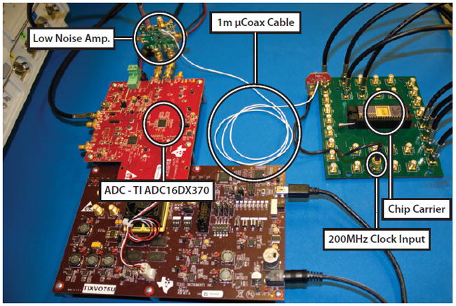
Equipment Setup for Testing TDM Multiplexing and ADC Capture Demultiplexing is Performed using RTL Simulation of FPGA
The TSMC multiplexer design described earlier in the paper has been fabricated and was used in the experimental setup. The silicon was diced and wire bonded to a chip carrier and connected to a generic PCB which brings each of the ICs connections out to SMA type connectors. The various bias voltages and power supplies required by the IC were connected to carefully decoupled power supplies to minimize noise. As the silicon design has no AFE, each of the inputs must also be biased to avoid saturation of the S/H buffers.
The output of the multiplexer was connected to a 1 m length of 48 AWG μCoax cable with 0.15 mm outer diameter, as could be used in a catheter application, to ensure the results take into account the realistic effects of a bandwidth limited channel. Furthermore, as the TDM clock signal must also be routed to the multiplexer and may potentially present crosstalk issues, the clock in this experiment was fed through a μCoax cable in the same bundle as the analog signal.
At the receiving end, a Texas Instruments LMH5401 LNA is used. This amplifier is connected using an evaluation module which has been modified to act as an active balun with 12 dB voltage gain. The amplifier input is AC coupled and configured to be single ended with input impedance approximately matched to the characteristic impedance of the cable. The impedance matching was performed in order to limit signal reflections which were causing large crosstalk issues in the earlier paper. The output of the amplifier was configured to be fully differential and connected directly to the input of a high speed ADC – a TI ADC16DX370EVM board. The ADC has an input bandwidth of 800 MHz, and a 16 bit resolution of which approximately 10 bits of resolution is used, though this will depend on the amplitude of the transducer signals.
As the hardware for interfacing the FPGA to the ADC has not yet been implemented, the data from the ADC has been captured using an evaluation module which interfaces the ADC with a PC via USB. The link training was performed by manually adjusting the phase between the ADC and TDM clocks which were produced by two high speed signal generators with a common reference clock. To complete the chain, the demultiplexing and processing of the data has been performed using the simulation model that was generated from the FPGA firmware design. The simulation model will exhibit exactly the same behavior as the targeted FPGA will, which makes the model a perfectly valid tool for processing experimental data.
For this design, a 200 MHz clock signal is used, which means that each of the 8 channels is sampled at 25 MSPS prior to being multiplexed. The frequency was chosen as a trade-off between sampling rate and the bandwidth requirements of the cable.
8 Results and Comparisons
Using the setup explained in VII, several experiments were performed in order to characterize the TDM silicon and the system as a whole. Of specific interest are two key points, firstly can ADC be synchronized correctly to allow the signals feeding the input of the TDM IC to be recovered using the direct digital demultiplexing approach, and secondly to determine how much crosstalk is present between channels as a result of distortion of the multiplexed signal through the cable.
During each test, signal generators were used to feed signals into either one channel, or multiple channels (with other channels receiving DC). Specifically, the tests involved using either a simple tone signal, or a more realistic sinc pulse. Using a tone allows for any crosstalk to be easily identified by analyzing the spectrum of each recovered signal – a spike at the frequency of the tone indicates that crosstalk is present. The sinc pulse allows for seeing the response of the system over the full bandwidth of each channel.
Fig. 8 shows the results from one of the experiments, in which only channel 1 of the eight was fed a signal, and the others tied to a DC bias. Fig. 8(a) and Fig. 8(b) show the recovered signal for the case of a 7 MHz tone, both in the time and frequency domain – the results are from the output of the FPGA simulation, which after the interpolation and decimation performed by the FPGA, are sampled at 50 MSPS. Fig. 8(c) and Fig. 8(d) show the recovered signal for the case of a sinc pulse with a bandwidth of approximately 11 MHz, again both in the time and frequency domain.
Figure 8.

Digitally Demultiplexed Experimental Results
As seen from Fig. 8(a), the tone has clearly been recovered in the demultiplexing process, with the FFT of the signal showing a clear spike at 7 MHz. There is some crosstalk occurring between channels as evidenced by the 7 MHz spike in Fig. 8(b) on the other channels which should have no signal. The level of the crosstalk signals is less than −40 dB when compared to the signal on channel 1. It should be noted that this is a measurement of the crosstalk between signals in the same μCoax cable as a result of the multiplexing scheme. The electrical crosstalk between the two separate μCoax cables in a catheter bundle was measured to be below −60 dB at frequencies up to 600 MHz, therefore it is the TDM crosstalk which represents the limiting factor in this scheme.
The frequency domain also shows clear spikes present at 3 MHz, 4 MHz, and 11 MHz, with smaller spikes at 8 MHz and 10 MHz also. It seems plausible that they are caused by aliasing within the multiplexer. For example, if the 7 MHz tone feeding the IC had some signal present at the second and third harmonics, this would account for two of the spikes (4 MHz and 11 MHz) as a result of aliasing. Investigation of into the cause of these spikes was not complete at the time the paper was submitted.
Observing the signal recovered from feeding in a sinc pulse, Fig. 8(c), the signal has also clearly been recovered correctly, with a fairly flat response across the pass band of the spectrum. The signals are band-pass filtered in the FPGA with cut-off frequencies of 3 MHz and 10 MHz resulting in the relatively empty spectrum outside this band. It is difficult to determine from the frequency domain in Fig. 8(d) what level of crosstalk is present between channels, however by measuring the peaks in the time domain, this crosstalk is roughly −36 dB – similar levels to the tone test.
These results show a significant improvement over those of the earlier work [26]. The source of this improvement is almost certainly the result of changes made at the receiving end, specifically the inclusion of an amplifier that has an input impedance closely matched to the characteristic impedance of the cable. This matching helps to reduce the amount of signal reflection in the cable which is one of the major sources of crosstalk between channels.
The crosstalk levels still appear to be large. However it is important to place these results in the context of the application. In a practical ultrasound imaging system, the input of the multiplexer would be connected to a transducer array in which each channel on the same multiplexer is an adjacent element. The variation in signal on adjacent channels of the multiplexer is much less than in these tests and as a result the channel to channel crosstalk can be significantly less. Furthermore, even at the presented crosstalk levels, the system would still provide suitable performance for ultrasound imaging catheters [33].
9 Conclusions
To produce 3D ICE catheters with large element counts, cable reduction is a key requirement not only to minimize the catheter diameter but also to allow operation under MRI where the risk of burns from induced heating in cables is a concern. While there are currently a large variety of cable reduction strategies, many of these are not suitable for this application due to size, power, or other limitations.
Time-division multiplexing coupled with direct digital demultiplexing presents an alternative reduction strategy which is well suited to the requirements of ultrasound catheters. This TDM approach has been developed and demonstrated in this paper. In the system design a cable reduction ratio of at least 8:1 can be achieved whilst allowing for simultaneous sampling of echo signals by sampling a time multiplexed signal at a very high sample rate. The signals were then in the digital domain using DSP techniques in RTL simulation of firmware for a high performance FPGA.
Experimental results have been obtained using a CMOS multiplexer fabricated in a 0.35 μm process coupled with a 1m length of narrow diameter μCoax cable and a high-speed ADC, and have been presented. These results demonstrate that the design is able to achieve a crosstalk between channels on the same cable of about −40 dB. This suggests the approach could provide suitable performance in an ultrasound imaging catheter while significantly reducing cable count.
References
- 1.Sugeng L, Shernan SK, Salgo IS, Weinert L, Shook D, Raman J, Jeevanandam V, Dupont F, Settlemier S, Savord B, Fox J, Mor-Avi V, Lang RM. Live 3-dimensional transesophageal echocardiography initial experience using the fully-sampled matrix array probe. J Am Coll Cardiol. 2008 Aug;52(6):446–449. doi: 10.1016/j.jacc.2008.04.038. [DOI] [PubMed] [Google Scholar]
- 2.Dausch DE, Gilchrist KH, Carlson JB, Hall SD, Castellucci JB, von Ramm OT. In vivo real-time 3-D intracardiac echo using PMUT arrays. IEEE Transactions on Ultrasonics, Ferroelectrics, and Frequency Control. 2014 Oct;61(10):1754–1764. doi: 10.1109/TUFFC.2014.006452. [DOI] [PubMed] [Google Scholar]
- 3.Brysiewicz N, Mitiku T, Haleem K, Bhatt P, Al-Shaaraoui M, Clancy JF, Marieb MA, Sugeng L, Akar JG. 3D Real-Time Intracardiac Echocardiographic Visualization of Atrial Structures Relevant to Atrial Fibrillation Ablation. J Am Coll Cardiol. 2014 Jan;7(1):97–100. doi: 10.1016/j.jcmg.2013.09.018. [DOI] [PubMed] [Google Scholar]
- 4.Ralovich K, John M, Camus E, Navab N, Heimann T. 6DoF Catheter Detection, Application to Intracardiac Echocardiography. 2014:17th International ConferenceMedical Image Computing and Computer-Assisted Intervention; 2014. pp. 635–642. [DOI] [PubMed] [Google Scholar]
- 5.Dempsey MF, Condon B, Hadley DM. Investigation of the factors responsible for burns during MRI. Journal of Magnetic Resonance Imaging. 2001;13(4):627–631. doi: 10.1002/jmri.1088. [DOI] [PubMed] [Google Scholar]
- 6.Gurun G, Tekes C, Zahorian J, Xu T, Satir S, Karaman M, Hasler J, Degertekin FL. Single-chip CMUT-on-CMOS front-end system for real-time volumetric IVUS and ICE imaging. IEEE Transactions on Ultrasonics, Ferroelectrics, and Frequency Control. 2014 Feb;61(2):239–250. doi: 10.1109/TUFFC.2014.6722610. [DOI] [PMC free article] [PubMed] [Google Scholar]
- 7.Bhuyan A, Choe JW, Lee BC, Wygant I, Nikoozadeh A, Oralkan O, Khuri-Yakub BT. 3D volumetric ultrasound imaging with a 32x32 CMUT array integrated with front-end ICs using flip-chip bonding technology. 2013 IEEE International Solid-State Circuits Conference Digest of Technical Papers (ISSCC); Feb 2013; pp. 396–397. [Google Scholar]
- 8.Moini A, Nikoozadeh A, Oralkan O, Choe JW, Sarioglu AF, Stephens DN, de La Rama A, Chen P, Chalek C, Dentinger A, Wildes D, Smith SL, Thomenius K, Shivkumar K, Mahajan A, O’Donnell M, Sahn DJ, Khuri-Yakub PT. Volumetric intracardiac imaging using a fully integrated CMUT ring array: Recent developments. 2011 IEEE International Ultrasonics Symposium (IUS); Oct 2011; pp. 692–695. [Google Scholar]
- 9.Lu Y, Tang H, Fung S, Wang Q, Tsai JM, Daneman M, El Boser B, Al Horsley D. Ultrasonic fingerprint sensor using a piezoelectric micromachined ultrasonic transducer array integrated with complementary metal oxide semiconductor electronics. Applied Physics Letters. 2015;106(26) [Google Scholar]
- 10.Murmann B. ADC Performance Survey 1997–2015. [Online]. Available: http://web.stanford.edu/~murmann/adcsurvey.html.
- 11.Krämer M, Janssen E, Doris K, Murmann B. 15.7 14b 35MS/S SAR ADC achieving 75dB SNDR and 99dB SFDR with loop-embedded input buffer in 40nm CMOS. 2015 IEEE International Solid-State Circuits Conference - (ISSCC); Feb 2015; pp. 1–3. [Google Scholar]
- 12.Savord B, Solomon R. Fully sampled matrix transducer for real time 3D ultrasonic imaging. 2003 IEEE Symposium on Ultrasonics; Oct 2003; pp. 945–953. [Google Scholar]
- 13.Matrone G, Savoia AS, Terenzi M, Caliano G, Quaglia F, Magenes G. A volumetric CMUT-based ultrasound imaging system simulator with integrated reception and μ-beamforming electronics models. IEEE Transactions on Ultrasonics, Ferroelectrics, and Frequency Control. 2014 May;61(5):792–804. doi: 10.1109/TUFFC.2014.6805693. [DOI] [PubMed] [Google Scholar]
- 14.Song TK, Greenleaf JF. Ultrasonic dynamic focusing using an analog FIFO and asynchronous sampling. IEEE Transactions on Ultrasonics, Ferroelectrics, and Frequency Control. 1994 May;41(3):326–332. [Google Scholar]
- 15.Stefanelli B, O’Connor I, Quiquerez L, Kaiser A, Billet D. An analog beam-forming circuit for ultrasound imaging using switched-current delay lines. IEEE Journal of Solid-State Circuits. 2000 Feb;35(2):202–211. [Google Scholar]
- 16.Yu Z, Pertijs MAP, Meijer GCM. Ultrasound beamformer using pipeline-operated S/H delay stages and charge-mode summation. Electronics Letters. 2011 Sep;47(18):1011–1012. [Google Scholar]
- 17.Rashid MW, Tekes C, Ghovanloo M, Degertekin FL. Design of frequency-division multiplexing front-end receiver electronics for CMUT-on-CMOS based intracardiac echocardiography. 2014 IEEE International Ultrasonics Symposium (IUS); Sept 2014; pp. 1540–1543. [Google Scholar]
- 18.Pahlavan K, Krishnamurthy P. Principles of Wireless Networks: A Unified Approach. Vol. 7. Prentice Hall; 2002. GSM and TDMA Technology; pp. 319–347. [Google Scholar]
- 19.Stern HPE, Mahmoud SA, Stern LE. Communication Systems: Analysis and Design. ch. 7. Pearson Prentice Hall; 2004. Multiplexing Techniques; pp. 362–387. [Google Scholar]
- 20.Spirit DM, Ellis AD, Barnsley PE. Optical time division multiplexing: systems and networks. IEEE Communications Magazine. 1994 Dec;32(12):56–62. [Google Scholar]
- 21.Lim J, Arkan EF, Degertekin FL, Ghovanloo M. Toward a reduced-wire readout system for ultrasound imaging. 2014, 36th Annual International Conference of the IEEE Engineering in Medicine and Biology Society (EMBC); Aug 2014; pp. 5080–5084. [DOI] [PMC free article] [PubMed] [Google Scholar]
- 22.Gurun G, Hasler P, Degertekin FL. Front-end receiver electronics for high-frequency monolithic CMUT-on-CMOS imaging arrays. IEEE Transactions on Ultrasonics, Ferroelectrics, and Frequency Control. 2011 Aug;58(8):1658–1668. doi: 10.1109/TUFFC.2011.1993. [DOI] [PMC free article] [PubMed] [Google Scholar]
- 23.Tekes C, Xu T, Carpenter TM, Bette S, Schnakenberg U, Cowell D, Freear S, Kocaturk O, Lederman RJ, Degertekin FL. Real-time imaging system using a 12-MHz forward-looking catheter with single chip CMUT-on-CMOS array. 2015 IEEE International Ultrasonics Symposium (IUS); Oct 2015. [Google Scholar]
- 24.Lemmerhirt DF, Borna A, Alvar S, Rich CA, Kripfgans OD. CMUT-in-CMOS 2D arrays with advanced multiplexing and time-gain control. 2014 IEEE International Ultrasonics Symposium (IUS); pp. 582–586. [Google Scholar]
- 25.Daft C, Panda S, Wagner P, Ladabaum I. Two Approaches to Electronically Scanned 3D Imaging Using cMUTs. IEEE Ultrasonics Symposium, 2006; Oct 2006; pp. 685–688. [Google Scholar]
- 26.Carpenter TM, Rashid MW, Ghovanloo M, Cowell D, Freear S, Degertekin FL. Time-division multiplexing for cable reduction in ultrasound imaging catheters. 2015 IEEE Biomedical Circuits and Systems Conference (BioCAS); Oct 2015. [Google Scholar]
- 27.Liu Q, Chen C, yao Chang Z, Prins C, Pertijs MAP. A mixed-signal multiplexing system for cable-count reduction in ultrasound probes. 2015 IEEE International Ultrasonics Symposium (IUS); Oct 2015. [Google Scholar]
- 28.Murmann B. A/D converter trends: Power dissipation, scaling and digitally assisted architectures. 2008 IEEE Custom Integrated Circuits Conference; Sept 2008; pp. 105–112. [Google Scholar]
- 29.Jonsson BE. A survey of A/D-Converter performance evolution. 2010, 17th IEEE International Conference on Electronics, Circuits, and Systems (ICECS); Dec 2010; pp. 766–769. [Google Scholar]
- 30.Manetakis K, Toumazou C, Papavassiliou C. A 120 MHz, 12 mW CMOS current feedback opamp. Proceedings of the IEEE 1998 Custom Integrated Circuits Conference; May 1998; pp. 365–368. [Google Scholar]
- 31.Serial Interface for Data Converters. JEDEC Committee JC-16 Std. 2012 Jan; [Online]. Available: http://www.jedec.org/standards-documents/results/jesd204.
- 32.Laakso TI, Valimaki V, Karjalainen M, Laine UK. Splitting the unit delay [FIR/all pass filters design] IEEE Signal Processing Magazine. 1996 Jan;13(1):30–60. [Google Scholar]
- 33.Oakley C, Mueller J, Dietz D, Kuhnke J. A minimally invasive ultrasound probe using non-coax cabling. 2001 IEEE Ultrasonics Symposium. 2001;2:1011–1016. [Google Scholar]