Abstract
This paper presents an energy-efficient oscillator for wireless sensor nodes (WSNs). It avoids short-circuit current by minimizing the time spent in the input voltage range from Vthn to [Vdd − |Vthp|]. A current-feeding scheme with gate voltage control enables the oscillator to operate over a wide frequency range. A test chip is fabricated in a 0.18 μm CMOS process. The measurements show that the proposed oscillator achieves a constant energy-per-cycle (EpC) of 0.8 pJ/cycle over the 21–60 MHz frequency range and is more efficient than a conventional current-starved ring oscillator (CSRO) below 300 kHz at 1.8 V supply voltage. As an application example, the proposed oscillator is implemented in a switched-capacitor DC–DC converter. The converter is 11%–56% more efficient for load power values ranging from 583 pW to 2.9 nW than a converter using a conventional CSRO.
Index Terms: Current starved, energy efficient, leakage based, low power, oscillator, switched-capacitor DC–DC, converter, wide frequency range, wireless sensor node (WSN)
I. Introduction
Wireless sensor nodes (WSNs) are an important part of the emerging Internet of Things [1], opening up new applications in areas related to medicine, infrastructure, and surveillance [2]-[5]. Recent trends in WSNs have focused on designing energy-efficient systems to realize energy autonomy using an energy harvester [6], [7]. For this goal, WSNs adaptively optimize themselves according to harvested energy, load power, and battery voltage condition using circuits such as voltage converters, dynamic frequency scaled circuits, and adaptive analog/RF circuits [7]-[12]. One adaptive technique involves changing the operation speed by modulating the clock frequency for optimum efficiency [10]-[12].
As an example, Fig. 1 shows a switched-capacitor DC–DC converter in a WSN with a lithium battery. It delivers power from a high battery voltage to a level where load circuits efficiently operate (e.g., 0.6 V for microprocessors [13] and 0.45 V for SRAM [14]). Its energy efficiency mainly depends on switching and conduction losses [15]. Switching loss arises from energy spent to charge (or discharge) parasitic capacitance and drive power switches. Conduction loss results from the on-resistance of power switches due to the Joule effect. As the operating frequency increases, the switching loss rises according to , whereas conduction loss decreases in the slow-switching limit (SSL) and becomes saturated in the fast-switching limit (FSL) [16]. The ideal operating point (i.e., that offering the highest efficiency) occurs at a frequency where the sum of those losses is minimized. However, this point varies according to the load power condition. For instance, the converter in [13] uses a switching frequency of 340 Hz for a 1–10 nW load power in standby mode, whereas it uses 335 kHz for 1–10μW loads in active mode.
Fig. 1.
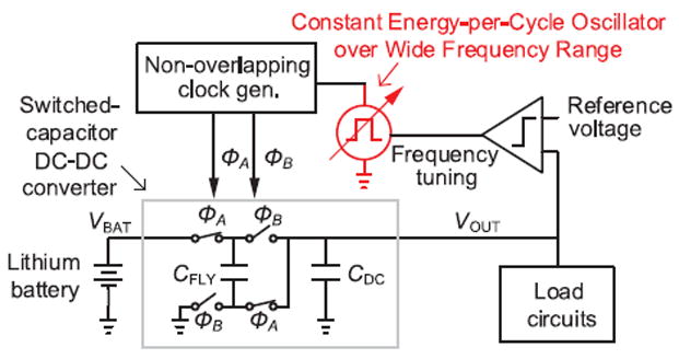
Capacitive step-down converter in a WSN with a lithium battery.
The oscillator in a WSN must not only cover a wide frequency range but also consume power proportional to the frequency, which becomes critical as the frequency is lowered. This quality ensures that the oscillator does not dominate the overall power at slow speeds and low load conditions. For this requirement, a ring oscillator is a good candidate due to its wide tuning range, small silicon area, and compact design. However, in ring oscillator circuits, the proportionality of power with frequency has not typically been considered as an important factor [17]-[23]. Although [24] proposed a ring oscillator that consumes power proportional to the frequency, the circuit was not verified in silicon, and its lowest frequency range is limited to 1.75 kHz.
This paper proposes a constant energy-per-cycle ring oscillator (CERO) in which the power is proportional to the frequency over a wide frequency range in order to maintain energy efficiency for adaptive circuits in WSNs. It is based on an oscillator topology that charges (or discharges) capacitance using the sub-threshold (weak inversion) current of a MOS transistor without short-circuit current [25]. The current and the oscillator are referred to as “leakage” and “leakage-based oscillator,” respectively, in this paper. The CERO employs a current-feeding scheme with gate voltage control in a leakage-based oscillator to efficiently control the output frequency. Due to the rapid escape from the voltage range between Vthn (NMOS threshold voltage) and [Vdd − |Vthp| (PMOS threshold voltage)], the oscillator power consumption scales linearly with the frequency by largely avoiding short-circuit current. The prototype oscillator is implemented in a standard 0.18 μm CMOS process. It achieves a constant 0.8 pJ/cycle over the 21 Hz–60 MHz frequency range at a power supply of 1.8 V, which is a higher efficiency than that of a current-starved ring oscillator (CSRO) below 300 kHz.
This paper is organized as follows. Section II describes a conventional CSRO and identifies its limitations in the targeted application space. Section III presents the proposed energy efficient oscillator, and Section IV reports the test chip measurement results. Section V shows an application example of a switched-capacitor DC–DC converter implemented with the proposed oscillator. Finally, Section VI concludes this paper.
II. Conventional CSRO
Fig. 2(a) shows a conventional CSRO [26]. Its delay stage consists of a delay generator (MX2 and MX3) and a current-starving circuit (MX1 and MX4). Charging (or discharging) current depends on the source-to-drain resistance of the current-starving circuit, which is controlled by its gate voltage (VBIASP and VBIASN). The gate voltage control enables the oscillator to tune the output clock frequency. An internal signal (N1) is connected to a logic inverter (MB1 and MB2) to buffer the output.
Fig. 2.
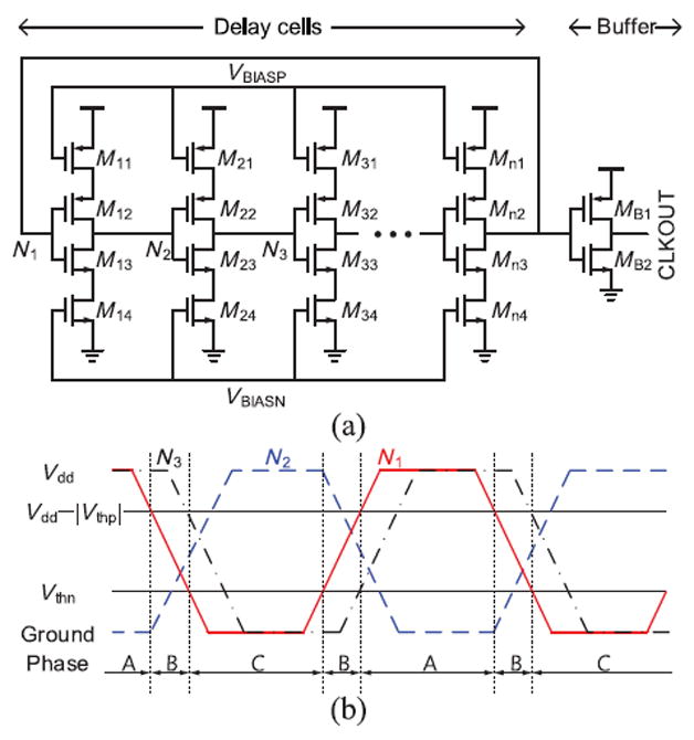
CSRO. (a) Circuit diagram. (b) Internal node waveforms.
Fig. 2(b) shows the simplified waveform of the internal nodes (N1, N2, and N3) in steady state. In Phases A and C, the first delay cell uses current only for charging or discharging its load capacitance since either M12 or M13 is turned off. In Phase B, however, V (N1) lies between Vthn and [Vdd − |Vthp|] and turns on both transistors, causing short-circuit current.
The current through the delay cells is limited by the current-starving transistor, and the limited current is proportional to the output clock frequency. Thus, the increased average power due to the short-circuit current through the delay cell scales with frequency and is acceptable, although the absolute power consumption is increased. However, the short-circuit current through the inverter buffer is not limited and significantly increases oscillator power consumption, as shown in Fig. 3. The output buffer dominates the total oscillator power below 1 MHz, since the short-circuit current through the buffer does not scale down at slower frequencies. For example, at 1.56 kHz clock generation, the buffer consumes 99.9% of the oscillator power. Thus, circuits using this oscillator cannot reduce their power consumption below 130 nW, even in a low-power standby mode.
Fig. 3.
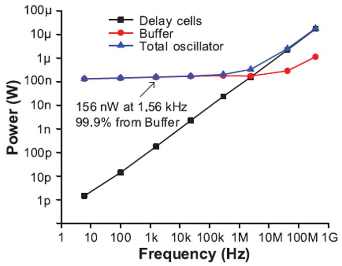
Simulated power consumption of a seven-stage CSRO with an inverter output buffer across frequencies.
III. Proposed Energy-Efficient Oscillators
A. Proposed CERO
To overcome the poor power scalability over frequency of CSROs, we propose a CERO, for which power scales linearly with frequency. Fig. 4(a) shows the circuit diagram of the delay cell. It uses leakage-based oscillator topology, which was initially designed for a fixed, slow frequency (e.g., 100 Hz with 10 pW) [25]. To adjust the output clock speed, a gate voltage control scheme is introduced.
Fig. 4.
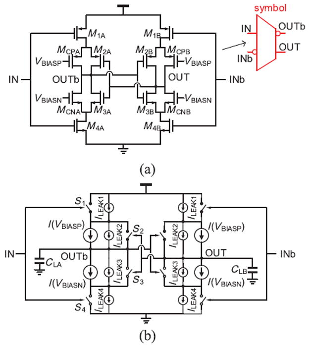
Delay cell of proposed CERO. (a) Circuit diagram. (b) Simplified model.
The delay cell includes input transistors (M1A, M1B, M4A, and M4B) and back-to-back inverters (M2A, M2B, M3A, and M3B). The input and output signals use differential configurations. The back-to-back inverters accelerate the changing output status to reduce short-circuit current. In addition, current control transistors (MCPA, MCPB, MCNA, and MCNB) are added to change the switching frequency by adjusting the charging and discharging currents.
The CSRO and CERO modulate their output frequencies in opposite manners. Specifically, CSRO changes its output frequency by limiting current, whereas the proposed approach for the CERO injects more current to change the frequency. To achieve a higher clock frequency, more charging (or discharging) current is added via the current control transistors. The oscillator frequency can potentially be modified using different load capacitances and transistor sizes, but a gate voltage control scheme is selected to minimize the overhead from additional capacitance.
Fig. 4(b) shows a simplified model of a delay cell of the proposed oscillator. The current control transistors are represented by current sources of I(VBIASP) and I(VBIASN), and the input transistors and back-to-back inverters are modeled by ideal switches with leakage current sources ILEAK1–4. CLA and CLB are the sum of the parasitic capacitance charged or discharged.
Fig. 5(a) shows the three-stage proposed oscillator as an example of a CERO. Two inverters are added as buffers for balanced output transitions. To better explain circuit operation, the condition without additional current (I(VBIASX) ≈ 0 A) is first discussed for simplicity. Based on the model shown in Fig. 4 (b), Fig. 5(b) and (c) shows the oscillator internal signals in steady state and the circuit behavior of the first stage delay cell, respectively. Here, N1A, N1B, N2A, and N2B are IN, INb, OUTb, and OUT of the first-stage delay cell in the oscillator, respectively. For simplification, only the left half of the circuit is displayed.
Fig. 5.
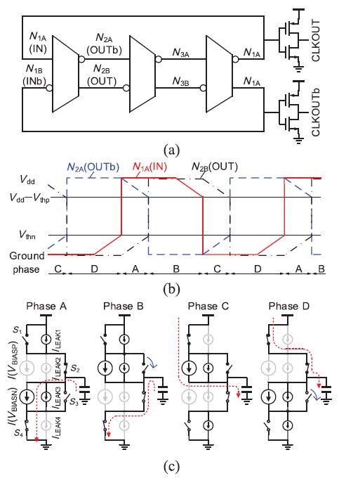
Three-stage proposed CERO. (a) Oscillator implementation. (b) Internal nodes. (c) Circuit status of a delay cell.
In Phase A, N2B (OUT) is lower than Vthn, and N1A (IN) becomes equal to the supply voltage. Thus, S2 and S4 are connected, whereas S1 and S3 are disconnected. There are two leakage paths: 1) comes from ILEAK3 and S4 and 2) derives from ILEAK1 and S2. Since Vds of M3A is larger than Vsd of M1A due to the high N2A (OUTb), the leakage path to ground dominates. Fig. 6(a) shows the simulated drain current of a minimum-size NMOS transistor with Vgs = 0 V. It shows that Ids = 0 A at Vds = 0 V, while Ids = 21 fA at Vds = Vdd − |Vthp|. The dependency of Ids on Vds can be found in the subthreshold current equation of the EKV model [27] (letting Vgs = 0 V) expressed as follows:
| (1) |
Fig. 6.
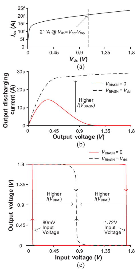
Simulated single delay cell. (a) Ids versus Vds (minimum-size transistor). (b) Output discharging current across output voltages. (c) Voltage transfer curve (Input: IN/Output: OUTb).
Here, μ is the mobility, Cox is the oxide capacitance, W is the transistor width, L is the transistor length, n is the slope factor (n ≡ dVg/dVp, where Vp is the pinchoff voltage), and UT is the thermal voltage (kT/q). Furthermore, the current can increase due to drain-induced barrier lowering (DIBL) and gate-induced drain leakage (GIDL) in advanced technologies.
Fig. 6(b) shows the output discharging current (the difference between the pull-down and pull-up current) in the single delay cell [Fig. 4(a)] when IN and INb are the supply voltage and ground, respectively. As the output voltage (OUTb) changes from the supply voltage to ground, the output discharging current is always positive, which guarantees the output voltage transition to ground. Similarly, the opposite input condition (0 V IN and 1.8 V INb) drives OUTb to the supply voltage. With higher additional bias current, I(VBIASN) or I(VBIASP), the current does not change its sign but only increases the amplitude, decreasing the charging or discharging time. The period of the oscillator mainly depends on the discharging current (ILEAK3 + IBIASN − ILEAK1), along with the output charging current (ILEAK2 + IBIASP − ILEAK4) in Phase C, which is the complementary of Phase A.
Fig. 6(c) shows the voltage transfer curve of the single delay cell. Its hysteresis becomes larger (up to 91% of the supply voltage) as the bias current is reduced. The output voltage transition happens when one of the input transistors becomes weaker than the transistors of the back-to-back inverters. For example, when N1A (IN) becomes 1.72 V in the beginning of Phase A, ILEAK1 equals ILEAK3. As N1A (IN) increases above 1.72 V, N2A (OUTb) decreases since M1A becomes weaker, and ILEAK1 < ILEAK3. Due to the hysteresis, the output transition is stable as the input voltage changes.
Phase B begins when N2A (OUTb) drops below [Vdd −|Vthp|] and N2B (OUT) rises above Vthn, turning on S3 (Fig. 5). Since N1A (IN) is still higher than [Vdd − |Vthp|], S4 is connected, whereas S1 is disconnected. This situation leads to the immediate discharging of CLA and charging of CLB (Fig. 4). S2 is connected in the beginning of the phase but disconnected as N2B (OUT) is charged above [Vdd − |Vthp|]. However, this situation does not affect the output voltage transition since the pull-down current is larger than the pull-up current, which is limited by ILEAK1 and turned off S1. The discharged output voltage (N2A, OUTb) increases the strength of M2B and raises the speed at which the complementary output voltage (N2B, OUT) is pulled up. The higher N2B (OUT) enhances the conductance of M3A and increases the speed at which N2A (OUTb) is pulled up. This positive feedback is formed by the back-to-back inverters that work as a latch and enable the rapid voltage transition. It helps effectively avoid short-circuit current in the oscillator itself and buffers by minimizing the time spent in the input voltage range between Vthn and [Vdd − |Vthp|]. Note that the short-circuit current through a buffer degrades energy efficiency in the conventional CSRO. Phases C and D are complementary to Phases A and B, respectively.
Since the voltage transition time in Phases B and D is negligible, the clock period of this oscillator is dictated by the sum of the discharging time of OUTb from Vdd to [Vdd − |Vthp|] (the charging time of OUT from ground to Vthn) during Phase A and the charging time of OUTb from ground to Vthn (the discharging time of OUT from Vdd to [Vdd − |Vthp|]) during Phase C. Due to the small leakage currents employed, this oscillator generates a clock with a long period. It can generate a slow clock with higher energy efficiency than CSRO since the short-circuit current issue is resolved, as described above.
To cover a wide frequency range, including higher frequencies, the oscillator output frequency can be modulated by controlling VBIASP and VBIASN and thus changing I(VBIASP) and I(VBIASN), respectively. This changes the charging (or discharging) slope of the internal voltages shown in Fig. 5(b) in the voltage range below Vthn or above [Vdd − |Vthp|]. As shown in Fig. 5(c), the supplemented current paths through the additional transistors increase the discharging current in Phase A and the charging current in Phase C. Hence, the discharging and charging currents become [ILEAK3 + I(VBIASN)− ILEAK1] and [ILEAK2 + I(VBIASP)− ILEAK4], respectively. Fig. 7 shows the simulated power consumption of the proposed CERO across frequencies, which demonstrates its power proportionality with frequency. Compared with the conventional CSRO (Fig. 3), the CERO achieves a constant energy-per-cycle (EpC) (0.3 pJ/cycle from 7.5 Hz to 128 MHz in simulation) by avoiding the short-circuit current through the buffer. Here, the EpC is the amount of required energy for one clock cycle, which is a commonly used figure-of-merit for energy-efficient oscillators [28], [29].
Fig. 7.
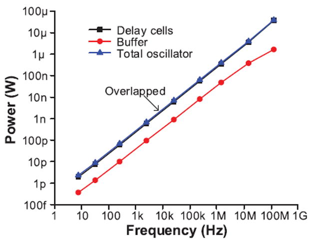
Simulated power consumption of a seven-stage proposed CERO with an inverter output buffer across frequencies.
B. Extension To CERO (Hybrid CERO)
The CERO achieves a power consumption that scales directly with the frequency. Compared with CSRO, however, its load capacitance is 7.7-fold larger (Fig. 8) due to the additional transistors and differential structure. Thus, as shown in Fig. 9, the CERO power is higher than that of CSRO above 1 MHz, where dynamic power dominates over short-circuit current.
Fig. 8.
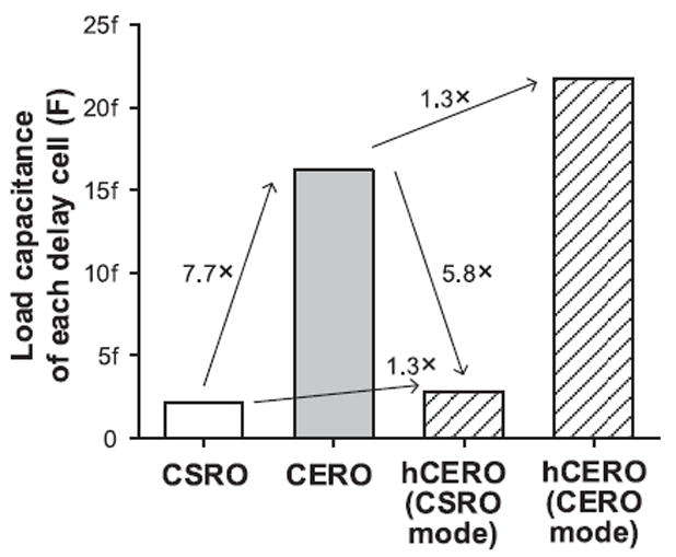
Simulated capacitance of each delay cell in CSRO, CERO, and hCERO.
Fig. 9.
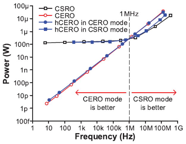
Simulated power consumption of CSRO, CERO, and hCERO across frequencies.
To address the higher energy consumption of the CERO at high frequencies, we therefore propose an extension to the CERO using a hybrid scheme referred to as the hCERO. The hCERO approach selectively employs one of two oscillator topologies by changing switch configuration, thereby achieving improved energy efficiency at high frequencies at the cost of additional complexity and area. Fig. 10(a) shows a delay cell for the hCERO. Five transistors (MS1 – MS5) are added to the basic CERO delay cell. By connecting all the switches in the CERO mode [Fig. 10(b)], this oscillator becomes equivalent to the CERO. In contrast, by disconnecting the switches in the CSRO mode [Fig. 10(c)], the circuit operates like CSRO. Half of a delay cell is disabled by a power gating switch (MS5), and back-to-back inverters are disassembled by disconnecting MS1 and MS2. The remaining active parts are the input and current control transistors, which provide CSRO functionality.
Fig. 10.
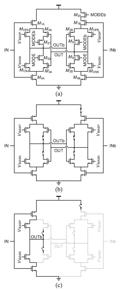
Proposed extension to the CERO (hCERO). (a) Circuit diagram of a delay cell. (b) CERO mode. (c) CSRO mode.
In the CSRO mode, the hCERO switches a 5.8 × lower load capacitance than the CERO (Fig. 8) due to the single-ended scheme. Due to the reduced switching capacitance, the hCERO in the CSRO mode is more efficient than the CERO above 1 MHz, where the impact of short-circuit current is not significant (shown in Fig. 9). The frequency breakpoint to switch between modes can be set when the oscillator is designed and placed in a simple lookup table.
C. Circuit Design
The oscillator maximum and minimum output frequencies depend on the size of the current control transistors. At the same time, additional switching capacitance reduces energy efficiency. Minimum width and length devices offer near-ideal maximum frequency with minimal EpC, as shown in Fig. 11. Note that using a 2 × larger transistor offers only a 2% increase in the maximum frequency at the expense of 17% in energy efficiency. Thus, the current control transistors are designed with the minimum width and length size. Furthermore, to reduce leakage current and switching capacitance, transistors for the inputs, back-to-back inverters, and mode switches are also implemented with the minimum size in both the CERO and the hCERO.
Fig. 11.
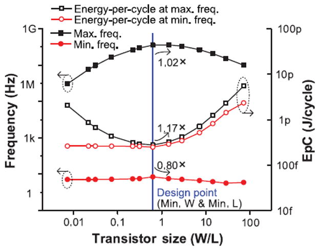
Simulated frequency and EpC of CERO across current control transistor sizes.
In the proposed oscillator, bias voltages are needed to set the voltage-controlled currents and hence the frequency. Fig. 12 shows the output frequency and generated bias current across the bias voltages. Of the frequency range in the log domain, 87% is covered by ≤ 0.8 V bias voltage since transistors operate in the weak-inversion region (Vth ≈ 0.7 V).
Fig. 12.
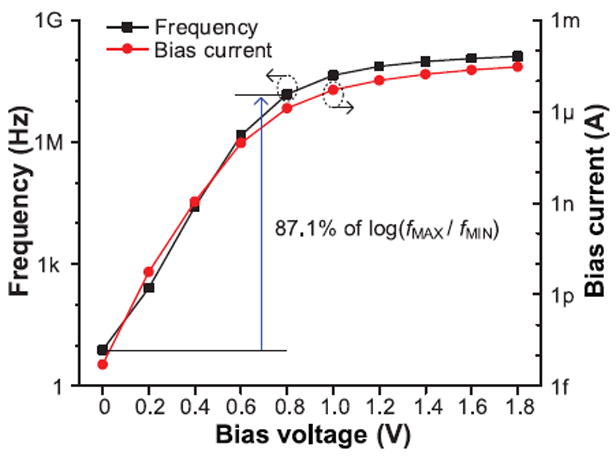
Simulated frequency and bias current of CERO across bias voltages.
Fig. 13 shows a simple bias voltage generator based on a voltage divider. The voltage divider uses stacked diode-connected transistors to generate different voltages that are used for bias voltages. One of the taps is connected to the gates of the current control transistors through a transmission gate-based multiplexer. In this design, same-sized transistors are used for the voltage division to minimize device mismatch.
Fig. 13.
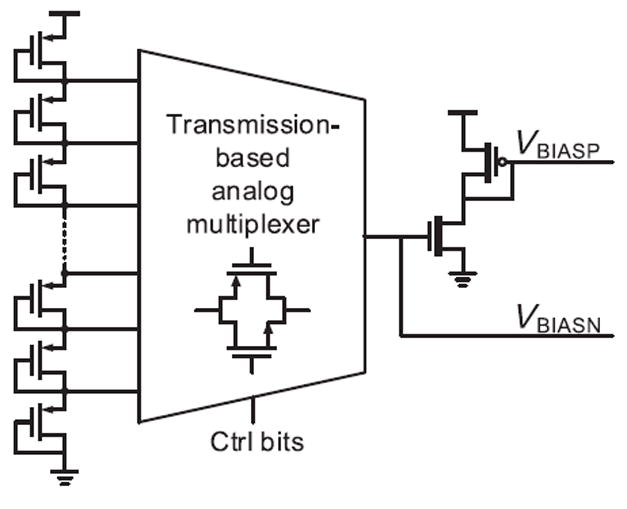
Voltage divider-based bias voltage generator.
Fig. 14 shows the bias voltage steps for different numbers of diode stacks and the frequency change per step at a bias voltage of ~ 0.35 V. The supply voltage and number of diode stacks determine the bias voltage step size. Considering an analog multiplexer implementation, 63 diode-connected transistors are used for the voltage divider, which offers a 28.6 mV voltage step and 1.97 × frequency change per step. The bias voltage generator is designed with high Vth transistors sized at 0.5/0.185 μm (W/L) and consumes 1.7 pW. With this low-power bias generator, the total power scales down with the frequency to 32 Hz, while maintaining an EpC between 0.27 and 0.33 pJ/cycle in simulation.
Fig. 14.
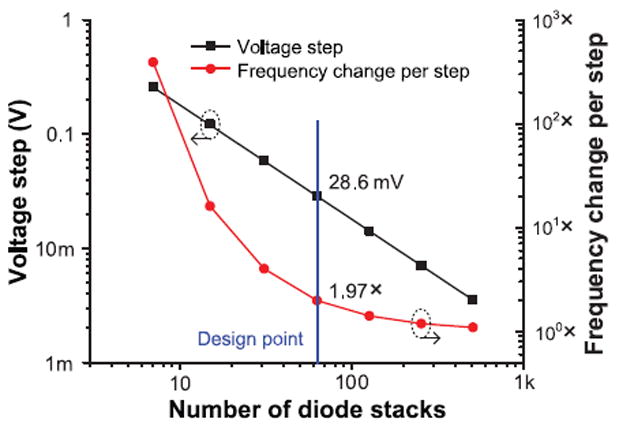
Simulated voltage step and frequency change per step of voltage divider-based bias voltage generator across numbers of diode stacks.
The voltage divider-based bias voltage generator achieves power scalability at low frequencies due to its extremely low power, but it results in significant variation in the output clock frequency in the face of temperature variation (551 × change across 0 °C–100 °C at a bias voltage of 0 V) and supply voltage change (1.31 M × across 0.3–3.3 V at bias voltage), as shown in Fig. 15. However, compared to CSRO with the same bias voltage generator, the frequency of the CERO demonstrates a similar sensitivity to temperature (< 0.98×) and supply voltage variation (< 1.34×). Three bias voltages are selected to set the output frequency to different levels. A voltage of 0 V is only used for the CERO, since the CSRO does not work without bias current.
Fig. 15.
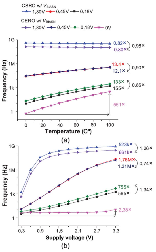
Simulated frequency variation on CSRO and CERO using a voltage divider-based bias voltage generator by (a) temperature variation (1.8 V supply voltage and TT corner) and (b) supply voltage variation (27 °C and TT corner).
Fig. 16 shows the output frequency and EpC from different corner simulations. The output frequency of the CERO [Fig. 16(a)] is sensitive to global process variation and can be changed by 171×. Compared to the CSRO, the CERO has a similar sensitivity to process variation (up to 2% ratio increase). On the other hand, the EpC of the CERO [Fig. 16(b)] is less sensitive to process variation (0.07 × at 0.18 V VBIASN) than the EpC of the CSRO due to the characteristics of a constant EpC. Although the output frequency changes, the EpC is maintained because the power consumption is proportional to the frequency. In addition, the CERO achieves a lower EpC than the CSRO at 0.18 and 0.45 V VBIASN by avoiding the short-circuit current through the output buffer; however, its EpC is higher at 1.8 V VBIASN due to more switching capacitance.
Fig. 16.
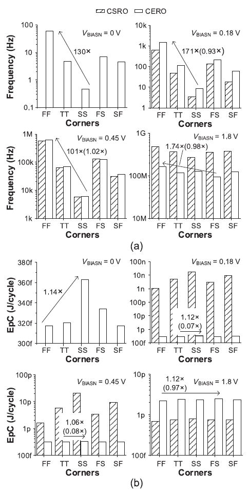
Corner simulations of CSRO and CERO (27 °C and 1.8 V supply voltage). (a) Oscillator frequency. (b) EpC [(): [Max./Min.] of CERO/[Max./Min.] of CSRO].
Fig. 17 shows the Monte Carlo simulation results with 1 k samples for each data point, including global process and local mismatch variation. The CSRO and CERO have the same size transistors. As shown in Fig. 17(a), the relative variations of the oscillator frequency (σ/μ) are similar for these two types of oscillators, with a higher σ/μ at lower bias voltage due to the deeper weak-inversion operating region of the transistors. Here, the logarithmic value of frequency is used, since its spread is closer to a normal distribution [Fig. 17(c)] than that of the raw value. The variation can be similar in the CERO and the CSRO since they have similar dominant variation sources in the slow frequency range, the current-starving transistors in the CSRO (MX1 and MX4 in Fig. 2) and current-controlling transistors in the CERO (MCPA, MCPB, MCNA, and MCNB). The CERO exhibits slightly less frequency variation than the CSRO (0.72 × at 0.18 V VBIASN), since the differential structure mitigates the impact of the variation. As shown in Fig. 17(b), the CERO has significantly less EpC variation than the CSRO due to the constant EpC across the oscillator frequencies. Fig. 17(c) and (d) shows the distribution of the frequency and EpC at 0.45 V VBIASN as examples.
Fig. 17.
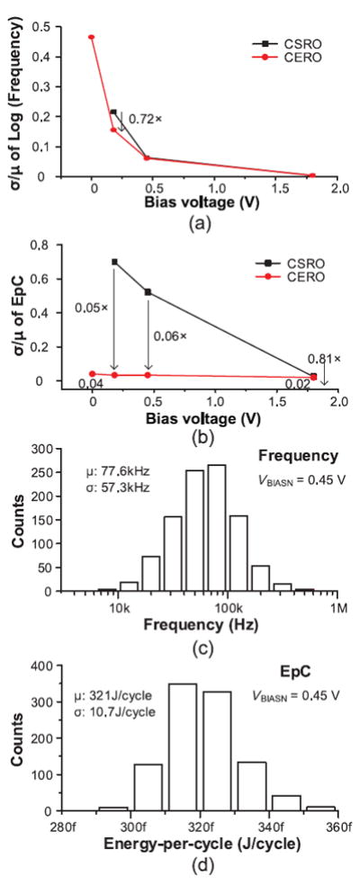
Monte Carlo simulations of CSRO and CERO (27 °C and 1.8 V supply voltage). (a) σ/μ of oscillator frequency. (b) σ/μ of EpC. (c) Histogram of oscillator frequency at 0.45 V VBIASN. (d) Histogram of EpC at 0.45 V VBIASN.
Compared to the CSRO, the CERO shows a similar sensitivity of the output frequency to temperature, supply voltage, process variation, and device mismatch. The frequency variation can be tolerated by a closed-loop design. For example, as seen in Fig. 1, the output voltage of a switched-capacitor DC–DC converter is compared to the desired reference voltage, and the clock frequency is updated to maintain the proper output voltage [10]. As will be seen later, the closed loop is implemented with off-chip equipment for a prototype switched-capacitor DC–DC converter, and the control bits of the multiplexer in the bias voltage generator are adjusted to find the desired oscillator frequency.
IV. Measurement Results
Prototype oscillators are fabricated in a 0.18 μm CMOS technology, including a seven-stage conventional CSRO and the proposed ring oscillators (CERO and hCERO) with inverter buffers for comparison (Fig. 18). A diode stack with PMOS transistors and a 64-input analog multiplexer using transmission gates are implemented to provide bias voltages for the oscillators. The oscillator outputs are connected to a frequency divider to allow for direct observation through a pad. The output frequency is manually changed by reconfiguring the control bits of the bias voltage generator shown in Fig. 13.
Fig. 18.
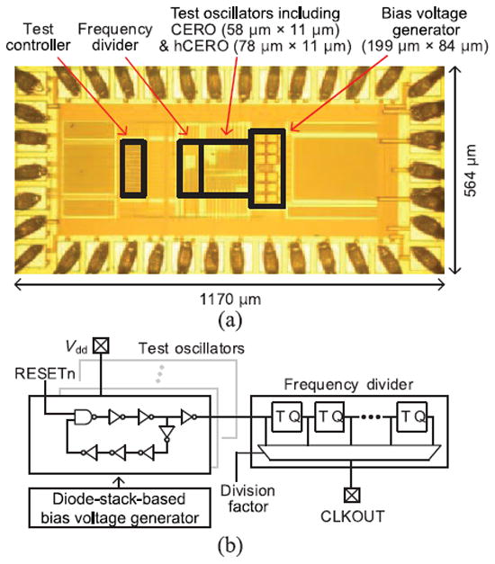
Test chip for oscillators. (a) Die photograph. (b) Test structure.
Fig. 19 shows the measured transient waveforms of the CERO. In Fig. 19(a), the minimum output frequency of 1.26 Hz is measured. In Fig. 19(b), the maximum frequency of 1.83 kHz is measured with the frequency divisions of 215, and the oscillator frequency is 60.0 MHz.
Fig. 19.
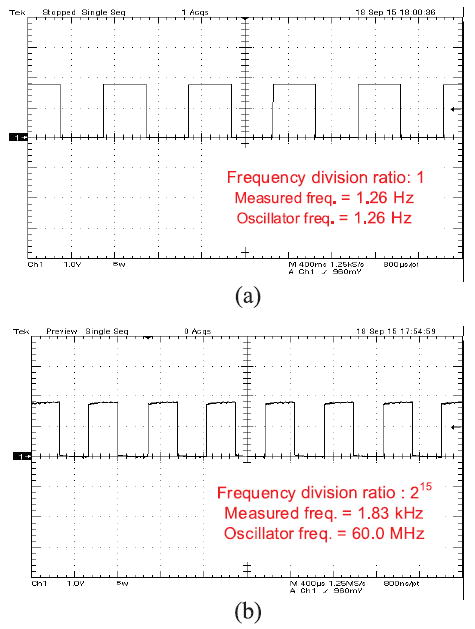
Measured waveforms from CERO. (a) Slowest output frequency with 0 V VBIASN. (b) Fastest output frequency with 1.8 V VBIASN.
Fig. 20 shows the measured power and EpC of the CSRO and the CERO. In Fig. 20(a), the CERO shows linearly scaled power consumption from 1.2 Hz to 60 MHz (fMAX/fMIN = 5 × 10⁷). In contrast, the CSRO power consumption has a floor at 144 nW due to short-circuit current through the buffer. In addition, it cannot effectively scale below 300 kHz, thereby excluding ultra-low frequency applications. This results in a much worse EpC for the CSRO at lower frequencies, as seen in Fig. 20(b). In contrast, the CERO shows a constant EpC of 0.8 pJ/cycle from 21 Hz to 60 MHz, which is enabled by the rapid transition through the voltage region causing short-circuit current. Below 300 kHz, the CERO requires less EpC than the CSRO, since the large short-circuit current through the buffer in the CSRO becomes dominant over dynamic energy. The difference between the simulated EpC (0.3 pJ/cycle, Fig. 16) and measured EpC (0.8 pJ/cycle, Fig. 20) results from the wire and coupling capacitance (91% increase, post-parasitic extraction) and higher ILEAK1 or ILEAK4 (Fig. 4) in fabricated devices compared with SPICE models.
Fig. 20.
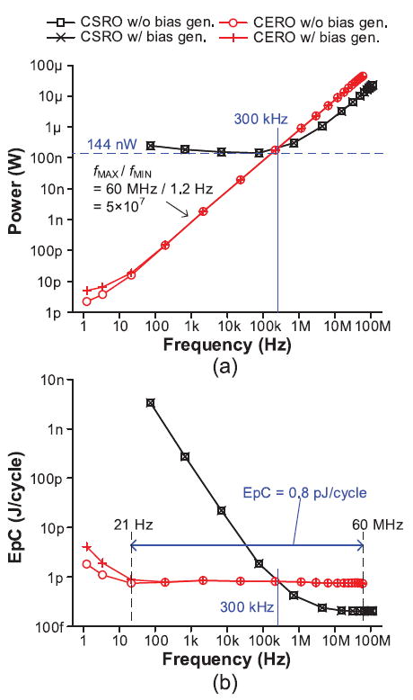
Measured power and EpC of CSRO and CERO. (a) Power. (b) EpC.
Fig. 21 shows the measured bias voltage profile of the CERO for a wide frequency generation. Most of the frequency range is covered at bias voltages less than the threshold voltage (~ 0.7 V) of the devices that control charging (or discharging) current. The high drain current sensitivity on gate voltage in the subthreshold region results in 1.14 × Hz/mV of frequency sensitivity on the gate voltage from 21 Hz to 1.2 MHz. Thus, this range should be well covered with fine steps by the bias voltage generator.
Fig. 21.
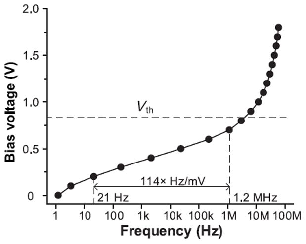
Measured bias voltage profile of CERO across frequencies.
Fig. 22 shows the measured maximum and minimum oscillator frequencies across temperatures or supply voltages. As shown in Fig. 22(a), the minimum frequency significantly changes (1147×) over the temperature range due to sub-threshold operation compared with the maximum frequency. This behavior results in a reduction in the frequency range (fMAX/fMIN) at higher temperatures, as shown in Fig. 22(b). In Fig. 22(c), the CERO operates down to 0.3 V, whereas the maximum supply voltage is limited by the process technology. For supply voltages above Vth, the maximum frequency becomes less sensitive to changes in the supply voltage, since the transistors begin to work in the strong-inversion region. As shown in Fig. 22(d), the frequency range increases from 101.5 to 107.8 as the supply voltage increases from 0.3–1.8 V, and it begins to saturate for supply voltages above 1.2 V.
Fig. 22.
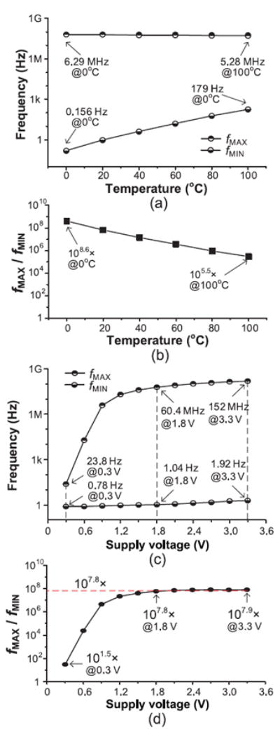
Measured frequency range of CERO. (a) fMAX and fMIN across temperatures (1.8 V supply voltage). (b) fMAX/fMIN across temperatures. (c) fMAX and fMIN across supply voltages (ambient temperature). (d) fMAX/fMIN across supply voltages.
Fig. 23(a) shows the measured oscillator frequencies from 10 different chips. Compared with the CSRO, the CERO has less frequency spread (< 83%). Fig. 23(b) shows the measured spread of EpC at 0.45 V VBIASN. The CERO has only 8% of the EpC spread observed with the CSRO due to the characteristics of a constant EpC as shown in the corner and Monte Carlo simulation results (Figs. 16 and 17).
Fig. 23.
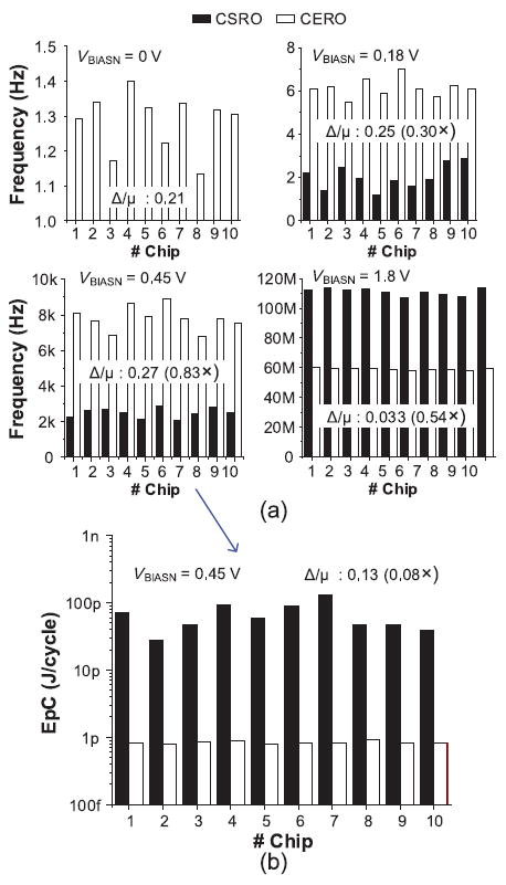
Measured CSRO and CERO from 10 chips (ambient temperature and 1.8 V supply voltage). (a) Oscillator frequency. (b) EpC [Δ: Max.–Min., (): Δ of CERO/ Δ of CSRO].
Fig. 24 shows the measured transient waveforms of hCERO. In Fig. 24(a), the minimum output frequency of 2.57 Hz is measured without frequency division in the CERO mode. In Fig. 24(b), the maximum frequency of 1.83 kHz is measured with frequency divisions of 215 in the CSRO mode. Thus, the oscillator frequency is 60.0 MHz.
Fig. 24.
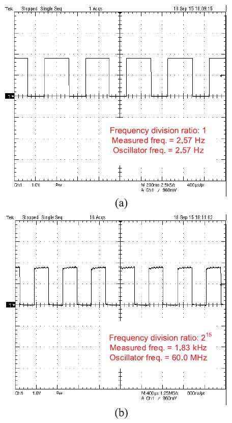
Measured waveforms from hCERO. (a) Slowest output frequency with 0 V VBIASN in CERO mode. (b) Fastest output frequency with 1.8 V VBIASN in CSRO mode.
Fig. 25 shows the measured power and EpC of the hCERO in the two different modes. Similar to the CERO, the hCERO in the CERO mode maintains an EpC of 0.7–1.2 pJ/cycle over the frequency range 35 Hz–51 MHz. Although the power reaches a minimum at 131 nW below 53 kHz, the CSRO mode is more efficient than the CERO mode above 200 kHz. Hence, the hCERO mode switches at 200 kHz to achieve lower EpC values.
Fig. 25.
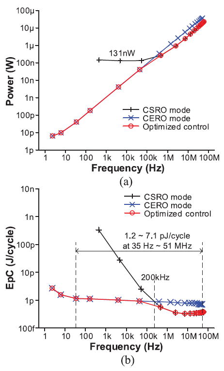
Measured performance of hCERO across frequencies. (a) Power. (b) EpC.
Fig. 26 shows the measured EpC of the CSRO, CERO, and optimized hCERO. Below 80 kHz, the hCERO has a higher EpC than the CERO by up to 38% (180 Hz). This finding results from 1.3× increased switching capacitance from additional transistors that control the mode change (Fig. 8). Above 80 kHz, the hCERO uses up to 56% less (7 MHz) EpC than the CERO. This is achieved by disabling half of the circuits in the delay cells, which reduces switching capacitance by 5.8×. However, although the hCERO operates in a similar manner as the CSRO, it is slightly less efficient than the CSRO at high frequencies due to the 1.3× capacitance penalty.
Fig. 26.
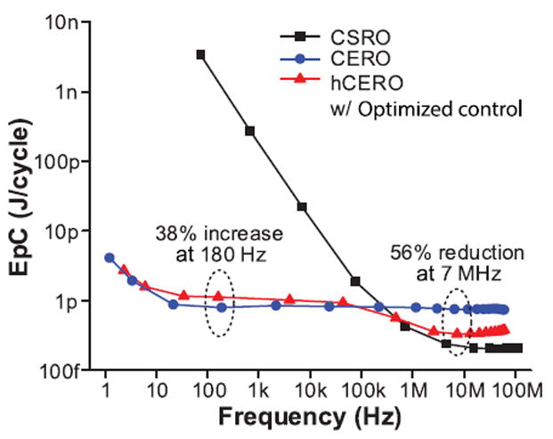
Measured EpC of CSRO, CERO, and hCERO.
Table I shows the performance summary of the proposed oscillators and prior wide range frequency ring oscillators. The CERO, along with [17], shows the widest range of frequency (> 7 orders of magnitude). However, [17] does not report energy/power at the lowest frequency, while the energy at the highest frequency is 2.8× higher than hCERO considering technology scaling such as capacitance and supply voltage (9.4× without considering technology scaling). Although [23] and [24] show good performance with respect to EpC, their frequency range is not nearly as wide as the CERO or the hCERO, and their oscillators are not verified in silicon. The CERO and the hCERO demonstrate good EpC over a wide frequency range.
Tabel I.
Performance Summary and Comparison to Other Prior Works
| This work | CSRO | [17] | [18] | [19] | [20] | [21] | [22] | [23] | [24] | ||
|---|---|---|---|---|---|---|---|---|---|---|---|
| CERO | hCERO | ||||||||||
| Process (nm) | 180 | 350 | 350 | 180 | 800 | 180 | 600 | 180 | 130 | ||
| Vdd (V) | 1.8 | 3.3 | 3.3 | 2 | 5 | 3.3 | 3.0 | 1.8 | 1.2 | ||
| fMAX (Hz) | 60 M | 61 M | 113 M | 256 M | 1.1 G | 807 M | 407 M | 368.9 M | 366 M | 6.9 G | 10 M |
| fMIN (Hz) | 1.2 | 2.3 | 74 | 4.8 | 4k | 20 M | 13 | 40 | 40 | 75 M | 1.75 k |
| log (fMAX / fMIN) | 7.7 | 7.4 | 6.2 | 7.7 | 5.4 | 1.6 | 7.5 | 7.0 | 7.0 | 2.0 | 3.8 |
| Power @ fMAX (W) | 44 μ | 23 μ | 23 μ | 1.76 m | N/A | N/A | 29.2 m | 30.05 m | 70 μ | 9.32 m | 3.6 μ |
| Power @ fMIN (W) | 5.1 p | 6.4 p | 247 n | N/A | N/A | N/A | N/A | N/A | 70 μ | 70 μ | 1 μ |
| EpC @ fMAX (J/cycle) | 0.73 p | 0.38 p | 0.20 p | 6.88 p | N/A | N/A | 71.7 p | 81.5 p | 0.19 p | 1.35 p | 0.36 p |
| EpC @ fMIN (J/cycle) | 4.25 p | 2.78 p | 3.34 n | N/A | N/A | N/A | N/A | N/A | 1.75 μ | 0.93 p | 0.57 p |
| Comments | Silicon measurement | Spice simulation | |||||||||
V. Application example
The proposed CERO is implemented to operate a switched-capacitor DC–DC converter fabricated in a 0.18 μm CMOS process, as shown in Fig. 27(a). A 6:1 step-down converter is designed to deliver power from a Li thin-film battery (~ 3.8 V) to a digital system such as a processor and a memory (0.5–0.6 V) for a low-power WSN.
Fig. 27.
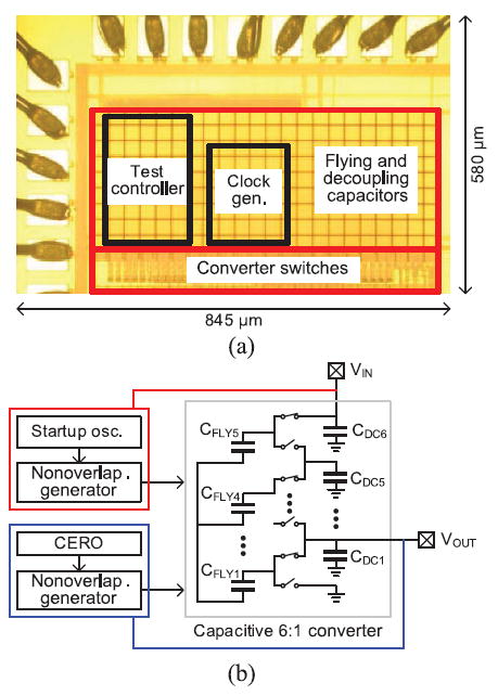
Test chip for a capacitive step-down converter. (a) Die photograph. (b) Converter diagram.
Fig. 27(b) shows the converter block diagram including the CERO. In the tradeoff between converter switching power and the drive strength of transistors, the gate-driving voltage is set to one-third of the input voltage (VIN). The converter switch drivers and the CERO operate under the same supply voltage, which is one tap of the converter (one-third VIN). Thus, the converter can operate by itself after it starts delivering power with the help of a startup oscillator that runs directly from the battery.
Fig. 28 shows the measured waveforms of the oscillator and DC–DC converter. In Fig. 28(a), 50 nA is loaded at the output of the DC–DC converter as default due to the input impedance of the oscilloscope (~ 10 MΩ). In Fig. 28(b), 50 µA is pulled down from the output by an off-chip resistor (~ 10 kΩ). The input voltage is 3.8 V.
Fig. 28.
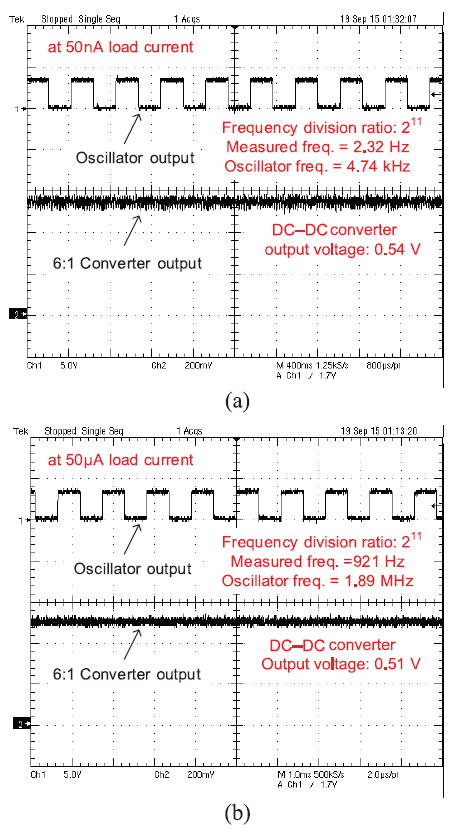
Measured waveforms from oscillator and DC–DC converter. (a) 50 nA load current. (b) 50 μA load current.
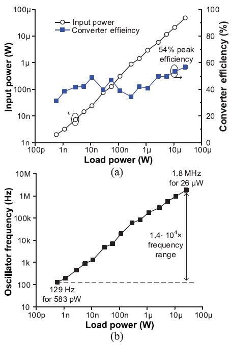
Fig. 29 shows the measured input power, converter efficiency, and clock frequency across load powers. The output voltage is monitored by a voltage meter (Keithley 2400), and LABVIEW automatically lowers the oscillator frequency by changing the control bits of the bias voltage generator until the output voltage decreases below 80% (0.5 V) of the zero-load output voltage. The converter can support a wide load power range from 583 pW to 26 μW and achieves a peak converter efficiency of 54%. As the load power decreases, the converter transfers less charge through the switched capacitor network. Hence, the switching speed can be slower, leading to lower input power with less switching and oscillator power. However, this is only true when the oscillator power scales with the frequency.
Fig. 29.
Measured converter across load powers. (a) Input power and converter efficiency. (b) Operating frequency.
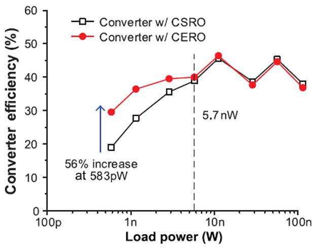
Fig. 30 shows the converter efficiency using either the CSRO or the CERO. The efficiency of the converter using the CSRO is calculated based on the oscillator measurement. Below 5.7 nW load power, the converter with the CERO is more efficient than the CSRO-based converter due to the power scalability of the CERO. The CERO-based converter efficiency is improved by 11%–56% for 583 pW–2.9 nW load power compared with that of the CSRO-based converter.
Fig. 30.
Efficiency of converters using CSRO and CERO.
VI. Conclusion
This work demonstrates an energy-efficient oscillator for WSN applications. In a prototype chip, the proposed CERO achieves a constant 0.8 pJ/cycle over a 21 Hz–60 MHz frequency range at a supply voltage of 1.8 V. Below 300 kHz, the CERO offers better energy efficiency than a conventional CSRO. This improved energy efficiency is enabled by the rapid transition through the voltage region between Vthn and [Vdd − |Vthp|] and the resulting substantial reduction in short-circuit current. The current-feeding scheme with gate voltage control offers a wide frequency range of 1.2 Hz–60 MHz. In addition, an extension to the CERO is proposed using a hybrid scheme (hCERO) to achieve improved energy efficiency at high frequencies with some costs in additional complexity and area.
Biographies
Inhee Lee (S’07–M’14) received the B.S. and M.S. degrees in electrical and electronic engineering from Yonsei University, Seoul, Korea, in 2006 and 2008, respectively, and the Ph.D. degree in electrical engineering from the University of Michigan, Ann Arbor, MI, USA, in 2014.
Currently, he is a Research Scientist with the University of Michigan. His research interests include energy harvesters, power management circuits, battery monitoring circuits, and low-power sensing systems for IoT applications.

Dennis Sylvester (S’95–M’00–SM’04–F’11) received the Ph.D. degree in electrical engineering from the University of California, Berkeley, CA, USA, in 1999, where his dissertation was recognized with the David J. Sakrison Memorial Prize as the most outstanding research in the UC-Berkeley EECS Department.
He is a Professor of Electrical Engineering and Computer Science with the University of Michigan, Ann Arbor, MI, USA, and Director of the Michigan Integrated Circuits Laboratory (MICL), a group of 10 faculty and more than 70 graduate students. He has held Research Staff positions in the Advanced Technology Group of Synopsys, Mountain View, CA, USA, Hewlett-Packard Laboratories in Palo Alto, CA, and visiting professorships at the National University of Singapore and Nanyang Technological University. He has authored over 375 articles along with one book and several book chapters. He holds 20 U.S. patents. He also serves as a Consultant and Technical Advisory Board Member for electronic design automation and semiconductor firms in these areas. He has Co-Founded Ambiq Micro, a fabless semiconductor company developing ultra-low power mixed-signal solutions for compact wireless devices. His research interests include the design of millimeter-scale computing systems and energy efficient near-threshold computing.
Dr. Sylvester serves on the Technical Program Committee of the IEEE International Solid-State Circuits Conference and previously served on the Executive Committee of the ACM/IEEE Design Automation Conference. He has served as Associate Editor for the IEEE Transcations on CAD and the IEEE Transactions on VLSI Systems, and Guest Editor for the IEEE Transactions on Circuits and Systems II. He received an NSF CAREER Award, the Beatrice Winner Award at ISSCC, an IBM Faculty Award, an SRC Inventor Recognition Award, and eight best paper awards and nominations. He is the recipient of the ACM SIGDA Outstanding New Faculty Award and the University of Michigan Henry Russel Award for distinguished scholarship.

David Blaauw (M’94–SM’07–F’12) received the B.S. degree in physics and computer science from Duke University, NC, USA, in 1986, and the Ph.D. degree in computer science from the University of Illinois, IL, USA, in 1991.
Since August 2001, he has been a Professor with the University of Michigan. He worked as the Manager of the High Performance Design Technology Group, Motorola, Inc., Austin, TX, USA. He has authored over 450 papers and holds 40 patents. His work has focused on VLSI design with particular emphasis on ultra-low power and high-performance design. He was the Technical Program Chair and General Chair for the International Symposium on Low Power Electronic and Design. He was also the Technical Program Co-Chair of the ACM/IEEE Design Automation Conference and a member of the ISSCC Technical Program Committee.
Footnotes
Color versions of one or more of the figures in this paper are available online at http://ieeexplore.ieee.org.
References
- 1.Ashton K. That ‘Internet of Things’ Thing. RFID J. 2009 Jul; [Online]. Available: http://www.rfidjournal.com/articles/view?4986#sthash.NsRaiwEl.dpuf.
- 2.Muller R, et al. A minimally invasive 64-channel wireless μECoG implant. IEEE J Solid-State Circuits. 2015 Jan;50(1):344–359. [Google Scholar]
- 3.Nazari MH, Mujeeb-U-Rahman M, Scherer A. An implantable continuous glucose monitoring microsystem in 0.18 μm CMOS. Proc IEEE Symp VLSI Circuits Dig; Jun, 2014. pp. 194–195. [Google Scholar]
- 4.Hu Y, et al. A self-powered system for large-scale strain sensing by combining CMOS ICs with large-area electronics. IEEE J Solid-State Circuits. 2014 Apr;49(4):838–850. [Google Scholar]
- 5.Kim G, et al. A millimeter-scale wireless imaging system with continuous motion detection and energy harvesting. Proc IEEE Symp VLSI Circuits Dig; Jun, 2014. pp. 178–179. [Google Scholar]
- 6.Mercier PP, Lysaght AC, Bandyopadhyay S, Chaandrakasan AP, Stankovic KM. Energy extraction from the biologic battery in the inner ear. Nat Biotechnol. 2012 Dec;3(12):1240–1243. doi: 10.1038/nbt.2394. [DOI] [PMC free article] [PubMed] [Google Scholar]
- 7.Jung W, et al. An ultra-low power fully integrated energy harvester based on self-oscillating switched-capacitor voltage doubler. IEEE J Solid-State Circuits. 2014 Dec;49(12):2800–2811. [Google Scholar]
- 8.Salem LG, Mercier PP. A recursive switched-capacitor DC–DC converter achieving 2n – 1 ratios with high efficiency over a wide output voltage range. IEEE J Solid-State Circuits. 2014 Dec;49(12):2773–2787. [Google Scholar]
- 9.Vidojkovic M, et al. A 0.33 nJ/b IEEE802.15.6/proprietary-MICS/ISM-band transceiver with scalable data-rate from 11 kb/s to 4.5Mb/s for medical applications. IEEE Int Solid-State Circuits Conf (ISSCC) Dig Tech Papers; Feb, 2014. pp. 170–171. [Google Scholar]
- 10.Bang S, Wang A, Giridhar B, Blaauw D, Sylvester D. A fully integrated successive-approximation switched-capacitor DC–DC converter with 31 mV output voltage resolution. IEEE Int Solid-State Circuits Conf (ISSCC’13) Dig Tech Papers; Feb, 2013. pp. 370–371. [Google Scholar]
- 11.Konijnenburg M, et al. Reliable and energy-efficient 1 MHz 0.4V dynamically reconfigurable SoC for ExG applications in 40 nm LP CMOS. IEEE Int Solid-State Circuits Conf (ISSCC’13) Dig Tech Papers; Feb, 2013. pp. 430–431. [Google Scholar]
- 12.Kim G, et al. A 695 pW standby power optical wake-up receiver for wireless sensor nodes. Proc IEEE Custom Integr Circuits Conf (CICC’12); Sep, 2012. pp. 9–12. [Google Scholar]
- 13.Lee Y, et al. A modular 1 mm3 die-stacked sensing platform with low power I2C inter-die communication and multi-modal energy harvesting. IEEE J Solid-State Circuits. 2013 Jan;48(1):229–243. [Google Scholar]
- 14.Ghaed MH, et al. Circuits for a cubic-millimeter energy-autonomous wireless intraocular pressure monitor. IEEE Trans Circuits Syst I Regul Papers. 2013 Dec;60(12):3152–3162. [Google Scholar]
- 15.Le H-P, Sanders SR, Alon E. Design techniques for fully integrated switched-capacitor DC–DC converters. IEEE J Solid-State Circuits. 2011 Sep;46(9):2120–2131. [Google Scholar]
- 16.Seeman MD, Sanders SR. Analysis and optimization of switched-capacitor DC–DC converters. IEEE Trans Power Electron. 2008 Mar;23(2):841–851. [Google Scholar]
- 17.Sheu M-L, Lin T-W, Hsu W-H. Wide frequency range voltage controlled ring oscillators based on transmission gates. Proc IEEE Int Symp Circuits Syst (ISCAS’05); May, 2005. pp. 2731–2734. [Google Scholar]
- 18.Hwang I-C, Kim C, Kang S-M. A CMOS self-regulating VCO with low supply sensitivity. IEEE J Solid-State Circuits. 2004 Jan;39(1):42–48. [Google Scholar]
- 19.Choi J, Lim K, Laskar J. A ring VCO with wide and linear tuning characteristics for a cognitive radio system. Proc IEEE Radio Freq Integr Circuits Symp (RFIC’08); Jun, 2008. pp. 395–398. [Google Scholar]
- 20.Zhao X, Chebli R, Sawan M. A wide tuning range voltage-controlled ring oscillator dedicated to ultrasound transmitter. Proc .16th Int Conf Microelectron (ICM’04); Dec, 2004. pp. 313–316. [Google Scholar]
- 21.Gupta N. Voltage-controlled ring oscillator for low phase noise application. Int J Comput Appl. 2011 Jan;14(5):23–27. [Google Scholar]
- 22.Nicodimus RA, Takagi S, Fujii N. Wide tuning range voltage-controlled ring oscillator. IEICE Trans Electron. 2003 Jun;E86–C(6):1085–1088. [Google Scholar]
- 23.Lei X, Wang Z, Shen L, Wang K. A large tuning range ring VCO in 180 nm CMOS. Proc Prog Electromagn Res Symp; Mar, 2013. pp. 1147–1149. [Google Scholar]
- 24.Veirano F, Pérez P, Besio S, Castro P, Silveira F. Ultra low power pulse generator based on a ring oscillator with direct path current avoidance. Proc IEEE 4th Lat Amer Symp Circuit and Syst (LASCAS’13); Feb, 2013. pp. 1–4. [Google Scholar]
- 25.Chen G, et al. Millimeter-scale nearly perpetual sensor system with stacked battery and solar cells. IEEE Int Solid-State Circuits Conf (ISSCC’10) Dig Tech Papers; Feb, 2010. pp. 288–289. [Google Scholar]
- 26.Hajimiri A, Limotyrakis S, Lee TH. Jitter and phase noise in ring oscillators. IEEE J Solid-State Circuits. 1999 Jun;34(6):790–804. [Google Scholar]
- 27.Enz CC, Krummenacher F, Vittoz EA. An analytical MOS transistor model valid in all regions of operation and dedicated to low-voltage and low-current applications. J Analog Integr Circuits Signal Process. 1995 Jul;8(1):83–114. [Google Scholar]
- 28.Denier U. Analysis and design of an ultralow-power CMOS relaxation oscillator. IEEE Trans Circuits Syst I Regul Papers. 2010 Aug;57(8):1973–1982. [Google Scholar]
- 29.Jee DW, Sylvester D, Blaauw D, Sim JY. A 0.45V 423nW 3.2 MHz multiplying DLL with leakage-based oscillator for ultra-low-power sensor platforms. Prc IEEE Int Solid-State Circuits Conf (ISSCC’13) Dig Tech Papers; Feb, 2013. pp. 188–189. [Google Scholar]


