

Abstract
Developing nanostructures with tunable magnetic states is crucial for designing novel data storage and quantum information devices. Using density functional theory, we investigate the thermodynamic stability and magnetic properties of tungsten adsorbed tri-vacancy fluorinated (TVF) graphene. We demonstrate a strong structure-property relationship and its response to external stimuli via defect engineering in graphene-based materials. Complex interplay between defect states and the chemisorbed atom results in a large magnetic moment of 7 μB along with high in-plane magneto-crystalline anisotropy energy (MAE) of 17 meV. Under the influence of electric field, spin crossover effect accompanied by a change in the MAE is observed. The ascribed change in spin-configuration is caused by the modification of exchange coupling between defect states and a change in the occupation of d-orbitals of the metal complex. Our predictions open a promising way towards controlling the magnetic properties in graphene based spintronic and non-volatile memory devices.
Understanding mechanisms that control magnetism at the nanoscale is crucial for designing novel spintronic and data storage devices. However, understanding these mechanisms remains an open challenge in material science, with a tremendous impact on today’s information technology1,2,3,4,5,6,7,8,9,10,11. Nanoscale magnetism is a complex interplay between magnetic anisotropy, exchange interactions, and quantum tunneling of magnetization, which in turn depend on the size, geometry, and composition of a nanostructure. One of the most promising methods to control the magnetic properties such as magneto-crystalline anisotropy energy (MAE) and magnetic moments of nanostructures is through an external electric field (e-field)12,13,14,15,16.
Graphene – a single sheet of carbon atoms has unique mechanical, electronic, and optical properties17,18, such as high mechanical strength, electronic mobility at room temperature17,19, long spin-relaxation lengths20,21, and most importantly the senstivity of its electronic properties toward an applied electric field22. These properties make graphene and its derivatives a potential candidate for spintronic and data storage devices. In graphene, carbon (C) atoms are sp2 hybridized in honeycomb geometry and exhibit a large surface area. The outer low-energy pz orbitals of C atoms can hybridize with the defect states modulating its electronic and magnetic properties22,23. While pristine graphene is nonmagnetic, the presence of certain types of defects can induce magnetism by breaking the balance between two sub-lattices and creating unpaired spins24,25,26. Defects such as vacancies27,28,29,30,31,32 and light adatoms like H, F and transition metal (TM) atoms have been found to induce magnetism in graphene33,34,35,36. However, the presence of thermal fluctuations can spin flip the states in spin-electronic devices, which can limit the practical applications of these materials. Therefore, a large MAE is required to preserve the magnetism in two-dimensional (2D) systems.
In general, MAE is an interplay among spin-orbit coupling (SOC), ligand field and surrounding environment (spatial and temporal symmetry). Thus, one can control the MAE and other magnetic properties by tuning these parameters5,37. Additionally, TM adatoms are found to have large SOC that can give rise to a large MAE. A large magnetic moment and magnetic anisotropy has been observed in Co adsorbed on graphene/Ru(0001) and Co on graphene/Ir(111) surfaces. The induction of magnetism in these system is due to the hybridization of graphene monolayer with the d-bands of adatom38. Pt-Ir, Os-Ru dimers and adatoms on graphene are found to have even larger MAEs39,40. However, TM adatoms on graphene tend to aggregate due to very small diffusion energies41,42. This aggregation can be counterbalanced by the presence of vacancies and extrinsic defects, at the same time inducing magnetism into the system43,44. Feng et al. synthesized reduced graphene oxide (RGO) by chemical exfoliation method and obtained fluorinated RGO by annealing RGO with XeF2. The fluorinated graphene is found to be stable and magnetic in the presence of vacancies45. The magnetism in such a system can be measured by using inelastic electron tunneling spectroscopy, where the magnetic moment, its orientation and MAE can be measured37,46.
As defects and doping play an important role in functionalizing graphene47, an intensive computational and experimental research has focused on designing new graphene based materials with fascinating physicochemical properties. In recent years, successful synthesis efforts have already been made for B, N and F doped graphene as well as other functional groups doped graphene, which are suitable for numerous technological applications48,49,50,51,52,53,54. Recent advances in first-principles based computational methods and high performance computing have given rise to efficient and powerful tools for in silico identification of promising defects/impurities with desired properties, and thereby investigating structure-property relationship.
In this work, we investigate the magnetic properties of W atom adsorbed on tri-vacancy fluorinated (TVF) graphene; a schematic picture is shown in Fig. 1(a). As shown in the figure, replacing one graphene ring by three electronegative fluorine atoms at alternate positions polarizes the system through a small charge transfer from W to neighboring C and F atoms. This leads to an overall anisotropic configuration, which results in a large magnetic moment and MAE in the system. Experimentally, such defects can be efficiently realized using a two-step process: adatom is deposited on graphene after creating desired number of vacancies using ion bombardment, pulsed laser or chemical vapor deposition55,56,57. Our study reveals that there is: (i) an induced magnetism in thermodynamically stable W adsorbed TVF graphene, (ii) spin crossover from high-spin to low-spin state under the application of an electric field and thereby the magnetization of the system can be tuned with an electric field, and (iii) a complex interplay between the defect states and chemisorbed metal atom that results in a large magnetic moment and a high in-plane MAE. These findings are of immense importance for designing data storage, non-volatile memory and spintronic devices. We also investigate the quantum mechanical origin of the change in the magnetic properties of W adsorbed TVF graphene with electric field.
Figure 1.

Top view of (a) an initial configuration, and (b) the relaxed structure of W chemisorbed TVF graphene; alternate carbon atoms are replaced by fluorine; (c) W adsorbed TVF graphene layer is placed in an external electric field. The yellow, red and blue spheres correspond to C, F and W atoms, respectively.
Results and Discussion
Thermodynamic Stability
Prior to investigate the physicochemical properties of W chemisorbed TVF graphene, we first investigate the thermodynamic stability of TVF graphene. Although nanoporous graphene2 and fluorine doped graphene51 have been successfully synthesized in experiments, there hasn’t been any theoretical study on the stability of fluorine doped trivacancy graphene. A necessary step for the atomic scale understanding of fluorine incorporation in a nanoporous graphene is the computation of energetics associated with the increasing fluorine content. In order to do that we calculate the defect formation energy (DFE) of fluorine doped graphene as,
 |
In Eqn. (1),  and
and  are the DFT total energies of considered pure graphene with six carbon vacancies and fluorine doped graphene sheets;
  is the DFT energy of an isolated F2 molecule and nF is the number of F atoms incorporated. The last term in Eqn. (1) describes the temperature (T) and partial pressure
  dependence of the chemical potential of fluorine molecule, which includes contributions from the translational, rotational and vibrational degrees of freedom of F2, and can be determined via statistical thermodynamics or from thermochemical JANAF Tables58.
Using ab-initio computations for fluorine doped graphene, the phase diagram showing the defect formation energetics as a function of F2 chemical potential (Δμ(F2)) is shown in Fig. 2(a). From the phase diagram, it can be seen that the doping of the nanoporous graphene with three F atoms is favored on a wide range of T- conditions. Figure 2(a) also suggests that Δμ(F2) for thermodynamically stable TVF graphene with three fluorine atoms lies between −2.45 to −1.85. In the inset of Fig. 2(a), DFE of nanoporous graphene is plotted as a function of the number of F atoms at the upper and lower bounds of Δμ(F2) of thermodynamically stable TVF graphene with three F atoms. To ensure the surface thermodynamic stability of the system under real-world synthesis conditions, (i.e. thermal annealing), the dependence of F2 chemical potential (Δμ(F2)) in the gas phase is translated to the pressure scale at 1100 K.
Figure 2.

(a) Defect formation energetics as a function of fluorine chemical potential (Δμ(F2)) for doping of F in graphene. The inset shows the defect formation energies of nanoporous graphene as a function of number of F atoms in the ring. (b) Total energy and total spin magnetic moment as a function of number of time steps at T = 290 K.
As depicted in Fig. 2, nanoporous graphene with three F atoms is the most stable configuration. Therefore, we consider TVF graphene, which creates a three-fold coordinated site for the adatom to be adsorbed. This can lead to profound changes in the magnetic properties of the system. We also checked the stability of W adsorbed TVF graphene as compared with other possible configurations. For example, we find that W adsorbed TVF graphene is 0.9 eV lower in energy than a WF3 molecule in vacuum and a nanoporous of six C vacancies in graphene. Thus, our calculations, as shown in the Fig. 2(a), confirm the feasibility of these defect formations and suggest experimental follow-up. Furthermore, the binding energy of W on TVF graphene is found to be −2.78 eV, which is calculated as,
 |
where  is the total energy of W atom, while
  and ETVF are the total energies of TVF graphene with and without adsorbed W atom, respectively.
In order to investigate the total energy and spin moment of the system at a finite temperature, we performed ab-initio MD simulations. In Fig. 2(b), we plot the total energy and spin magnetic moment of the system as a function of time at T = 290 K. We find an almost constant energy and a stable ferromagnetic state over the time at T = 290 K, which confirms that the system (W adsorbed TVF graphene) is dynamically stable. We also tested the ferromagnetic stability at room temperature (T = 300 K) for a few hundred steps and found the system to be stable at room temperature and showing FM properties.
Magnetic Moment
As shown in Fig. 1(a), the dangling bonds unoccupied by F atoms in nanoporous graphene are denoted as C1, C2, and C3. A stable structure after the relaxation process is achieved as a consequence of the repulsion between F atoms and un-bonded carbon atoms that results in W atom getting bonded with one of the un-bnded carbon atoms and breaking the symmetry of the system. This results in lowering the energy of the system and a Jahn-Teller distortion in the system. The geometrical reconstruction of dangling bonds results in symmetry breaking that results in the total spin magnetic moment of the system to be 7 μB. The physical origin of high spin magnetic moment can be inferred from the high-spin configuration of 5d-series W (d5↑, d0↓, s1↑, s0↓) adatom on TVF graphene.
The valence states of 5d-TM atoms have filled 6s orbitals and partially filled, half filled or completely filled d-orbitals. The electronic configuration of W atom is 5d5↑, 6s1↑. Adsorption of W atom on TVF graphene leads to a rise in the energy of 6s orbitals, which is then minimized through the polarization of 6s orbitals by transferring the charge from 6s to the minority states of 5d-orbitals59,60. The covalent bonding between W atom and TVF graphene results into charge transfer from the W to carbon and fluorine atoms as evident from the spin density profile shown in Fig. 3(a); this in turn decreases the magnetic moment of W. From the figure we also find that the W adatom is bonded to one of the carbon atoms (C3). The other two dangling bonds remain unsaturated and induce a finite magnetic moment of 0.70 μB/dangling bond which is same as the magnetic moment of the dangling bonds in absence of the adatom. As W is bonded to one of the dangling bonds by hybridization only, most of the uncompensated charges need to be accommodated on W atom itself, which leads to a large moment of 3.70 μB per W atom. Note that this spin magnetic moment is greater than the magnetic moment of 2.29 μB previously found for W adatom on di-vacancy nitrogenized graphene40.
Figure 3.
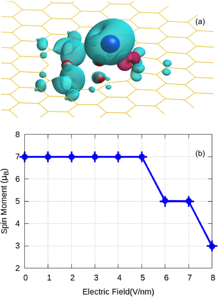
(a) Spin density profile of W adsorbed TVF graphene, (b) Variation of the total spin moment of the system as a function of electric field, without including spin-orbit coupling in the system.
To check the stability of the hybrid system at high electric fields, we calculate its cohesive energy in the absence and presence of e-field. The calculated cohesive energy per atom of W adsorbed TVF graphene at zero and 6V/nm e-fields are 7.66 and 7.67 eV, respectively. These cohesive energies confirm that the defect can withstand high electric fields. The change in spin magnetic moment of W adsorbed TVF graphene as a function of electric field is shown in Fig. 3(b). Magnetic moment of the system remains constant in the range of 0–5 V/nm e-fields. In this range, both the neighboring dangling bonds are ferromagnetically coupled. However, beyond 5 V/nm, the spin of C2 couples antiferromagnetically with C1 in the neighboring ring due to change in the occupation of states of both the dangling bonds. This results in decrease in the magnetic moment of the system. Thus the magnetic moment of the hybrid system jumps from a high-spin value to a low-spin value as the electric field changes from 5 to 6 V/nm resulting in a spin crossover effect. As the high- and low-spin states describe the different magnetic states, switching between the two states with an e-field can be used to increase the efficiency and sensitivity of magnetic memory devices.
Quantum mechanically, magnetism of dangling bonds arises primarily from the un-bonded sp2 orbitals, however a small fraction of this moment also comes from the spin polarized π-orbitals. The electric field shifts the lower edge of the minority states towards the Fermi level, which leads to a decreased magnetic moment contribution by dangling bonds and therefore reduction in the total moment of the system as can be seen in Fig. 3(b). At and beyond an electric field of 8 V/nm, spins of both the dangling bonds couple antiferromagnetically with the W atom and there is also a decrease in the spin moment of W atom due to a change in the occupation of d-orbitals. This further decreases the total spin moment of the system. Thus, through electric field, one can control the alignment of spins on carbon atoms in the defect region. Although the electric field affects the magnetic moment of W, the effect is greater on dangling bonds where the coupling of dangling bonds changes from the ferromagnetic to antiferromagnetic.
Magnetic Anisotropy
Despite the large magnetism, the use of any given material in spintronic devices also depends upon its MAE as it decreases the thermal fluctuations in the magnetization of the system. The estimated energy differences for W adsorbed TVF graphene between different magnetization directions are: ΔExz(Ex–Ez) = −7.95, ΔEyz(Ey–Ez) = −17.19 and ΔExy(Ex–Ey) = 9.25 meV. This suggests that the easy axis of magnetization lies in the plane of the graphene (along y-axis) and hard axis is perpendicular to the surface lying along the z-axis with an MAE of 17.19 meV. Energy differences between principal magnetization directions are plotted in Fig. 4(a). We find that although MAE depends upon the occupations of states of the system, here electric field has no significant effect on the MAE (Ey–Ez) until the applied e-field reaches 6 V/nm. Beyond the e-field of 6 V/nm, a gradual variation in MAE has been observed as shown in Fig. 4(a). At an e-field of 8 V/nm, the corresponding energy differences are: Ex–Ez = −7.20, Ey–Ez = −12.93 and Ex–Ey = 5.72 meV. Hence, despite the decrease in the energy differences, the easy and hard directions of magnetizations remain unchanged.
Figure 4.
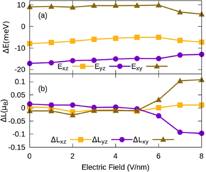
Effect of electric field on the (a) energetics and (b) orbital moment along three principal magnetization directions in W adsorbed TVF graphene. Eij and ΔLij are defined in the text.
Change in the occupation of d-orbitals and change in the orbital moment can affect the values of MAE5,61. The change in orbital moment with respect to orientation of the magnetization vector from one direction to other namely ΔLxz (Lx–Lz), ΔLyz (Ly–Lz) and ΔLxy (Lx–Ly), in presence of SOC is plotted in Fig. 4(b). Note that ΔLyz (Ly–Lz) is negative beyond an e-field of 5 V/nm and increases gradually indicating an increase in the orbital moment along the z-direction, which would suggest an easy direction of magnetization to be along z-direction. However, since this difference is small (<0.1 μB), it is difficult to predict the direction of easy axis based only upon the difference in orbital moment62. The discrepancy can be inferred from the fact that the energy induced by SOC matrices below and above the Fermi level is no longer proportional to the projection of magnetization vector on orbital angular momentum. However, beyond 5 V/nm, a positive and gradual increase in ΔLxy (Lx–Ly) and ΔLxz (Lx–Lz) suggests a switching of MAE at higher electric field. Inclusion of SOC suppresses the magnitude of spin moment, however it has the same trend as the non-SOC case shown in Fig. 3(b). This is due to the directional dependence of the magnetization vector.
To obtain a quantum mechanical picture of the origin of magnetism and MAE, in Fig. 5 we plot the total and partial orbital density of states (PDOS) of W adatom in Fig. 5. We see that electric field pushes the majority states towards Fermi level, which changes the occupation of states resulting in a change in magnetic moment and MAE. The MAE in a physical system arises due to (i) the splitting of degenerate partially occupied eigenstates connected through SOC and (ii) by coupling of the states above and below the Fermi level (unoccupied and occupied) through SOC matrix elements5. Quantitatively, within second order perturbation, MAE can be expressed as:
Figure 5. Orbital projected spin-polarized density of states of W adatom on TVF graphene with and without external electric field.

The electric field is in V/nm.
 |
where 〈 and
and  〉 are the occupied and unoccupied eigenstates, respectively; Lz and Ly (Lx) are the angular moment operators along the principal axes. As, Eqn. 3 contains energy difference between the unoccupied and occupied states in the denominator; states near the Fermi level will result in a large contribution to Eqn. 3 and the MAE will increase.
The DOS in Fig. 5 also reveal that in the absence of e-field the coupling between dzx and dx2–y2 and the coupling between dz2 and dxz through Ly have dominant contribution to Eqn. (3), which forces the easy axis to be in-plane along y-axis. Although application of electric field increases the coupling between (dzx, dx2–y2) and (dz2, dxz) orbtials, we find a decrease in the MAE of the system at higher fields. This decrease is found to be due to the increase in the coupling interaction of (dxy, dx2–y2) and (dxz, dyz) orbitals through Lz61. At higher fields, change in the direction of MAE from y- to x-axis is expected to be due to the coupling of dxy with dxz, coupling of dx2–y2 with dyz and the coupling of dz2 with dyz orbitals realized through Lx operator.
To check the robustness of presented results with respect to the change in exchange correlation potential, we also performed DFT calculations using PBE-sol pseudopotentials. We find that both PBE and PBE-sol yield similar results for structure and magnetism in the absence of SOC at all the fields. Upon inclusion of SOC, the computational cost of calculations increases, therefore we calculated the MAE and orbital moments just at the smaller fields and found that the results change by 2–3 meV, however the overall trend remains the same.
Conclusions
In summary, we have investigated the magnetic properties of tungsten adsorbed on nanoporous TVF graphene and have demonstrated the influence of intrinsic defects on the stabilization of the adatom and inhibition of aggregation. Our computational results suggest that the proposed defect is thermo-dynamically and geometrically stable and can be fabricated with existing experimental techniques. Further, we predict that the magnetic properties of the hybrid system can be modified using e-field via the changes in the occupation of W adatom states. As a result of this modulation, we find a switching between high-spin and low-spin states after an e-field of 5 V/nm. Present study also confirms an easy plane anisotropy accompanied by spin crossover in tungsten adsorbed on TVF graphene, which is an important result for non-volatile memory and spintronic devices. Further, we expect to see a change in the direction of magnetization at higher fields or by substituting different adatoms. We believe that our results will stimulate experimental work on these kinds of hybrid systems to develop highly efficient data storage and spintronic devices based on graphene.
Computational Details
Density functional theory calculations are performed using frozen core projector augmented wave method as implemented in Vienna Ab-Initio Simulation Package (VASP)63,64. Exchange and correlation interactions are modeled using generalized gradient approximation with the Perdew-Burke-Ernzerhof (PBE) functional65. To expand the crystal wave functions, a plane wave basis cutoff of 520 eV is used. To accurately estimate the MAE, SOC is used in a noncollinear mode66. An energy convergence threshold of 10−7 eV and a Γ centered k-mesh of size 7 × 7 × 1 is used to sample the Brillouin zone of the system67. The geometrical structure is constructed using 7 × 7 × 1 sized supercell.
As demonstrated in the Fig. 1(a), to create TVF graphene a ring containing six carbon atoms is removed and three strong ligand atoms like fluorine are doped at alternate positions. W atom is placed at the center of the ring having 3Dh symmetry. The other three C atoms in the ring remain non-bonded and are called as dangling bonds. The relaxation breaks the 3Dh symmetry of the system and the W atom shifts towards one of the carbon atoms, as depicted in Fig. 1(b). The structural relaxation is performed until all the forces on atoms are smaller than 0.001 eV/Å. To study the electric field response of the system, we used dipole layer method68 as shown in Fig. 1(c).
To check the stability of W adsorbed TVF graphene system, we also performed finite temperature ab-initio molecular dynamic (MD) simulations using Nose-Hoover heat bath scheme69 at 290 K and 300 K to check the stability of the system near and at room temperature for 850 steps. The time step between consecutive steps was set to be 1fs.
Additional Information
How to cite this article: Kumar, P. et al. Tunable magnetism in metal adsorbed fluorinated nanoporous graphene. Sci. Rep. 6, 31841; doi: 10.1038/srep31841 (2016).
Acknowledgments
This research is supported by the Research Corporation’s Cottrell College Science award (Grant No. 20234) and NSF CAREER award (DMR-1255584). We are thankful to the HPC center of Idaho National Laboratory for computational support where, most of the calculations are performed. Work by VS and FAR was supported by the U.S. Department of Energy, Office of Science, Basic Energy Sciences, Materials Sciences and Engineering Division. VS acknowledges the XSEDE computational resource allocation number TG-DMR160051.
Footnotes
Author Contributions P.K., R.P. and V.S. developed the concept. P.K. and V.S. performed the simulations and data analysis. The obtained results were discussed with R.P., F.A.R. and L.-M.Y. P.K., V.S. and R.P. wrote the manuscript. All the authors contributed to interpretation and discussion of the data and commented on the manuscript.
References
- Zhou W., Lee J., Nanda J., Pantelides S. T., Pennycook S. J. & Idrobo J.–C. Atomically localized plasmon enhancement in monolayer graphene. Nat. Nano. 7, 161–165 (2012). [DOI] [PubMed] [Google Scholar]
- Tsymbal E. Y., Electric toggling of magnets. Nat. Mater. 11, 12–13 (2012). [DOI] [PubMed] [Google Scholar]
- Zhou W., Kapetanakis M. D., Prange M. P., Pantelides S. T., Pennycook S. J. & Idrobo J.–C. Direct determination of the chemical bonding of individual impurities in graphene. Phys. Rev. Lett. 109, 206803-1-5 (2012). [DOI] [PubMed] [Google Scholar]
- O’Hern S. C., Boutilier M. S. H., Idrobo J. C., Song Y., Kong J., Laoui T., Atieh M. & Karnik R. Selective ionic transport through tunable subnanomater pores in single layer graphene membranes. Nano Lett. 14, 1234–1241 (2014). [DOI] [PubMed] [Google Scholar]
- Skomski R. Nanomagnetics. J. Phys.: Cond. Matt. 15, R841–R896 (2003). [Google Scholar]
- Han W., Kawakami R., Gmitra M. & Fabian J. Graphene Spintronics. Nat. Nano. 9, 794–807 (2014). [DOI] [PubMed] [Google Scholar]
- Hirohata A. & Takanashi K. Future Perspectives for Spintronic Devices. J. Phys. D: Appl. Phys. 47, 193001-1-40 (2014). [Google Scholar]
- Wolf S. A., Lu J., Stan M. R. & Chen E. The Promise of Nanomagnetics and Spintronics for Future Logic and Universal Memory. Proc. of IEEE 98, 2155–2168 (2010). [Google Scholar]
- Skomski R., Manchanda P., Kumar P., Balamurugan B., Kashyap A. & Sellmyer D. Predicting the Future of Permanent-Magnet Materials. IEEE Trans. Magn. 49, 3215-1-6 (2013). [Google Scholar]
- Wang W.-G., Li M., Hageman S. & Chien C. L. Electric-field-assisted switching in magnetic tunnel junctions. Nat. Mater. 11, 64–68 (2012). [DOI] [PubMed] [Google Scholar]
- Shiota Y. et al. Induction of coherent magnetization switching in a few atomic layers of FeCo using voltage pulses. Nat. Mater. 11, 39–43 (2012). [DOI] [PubMed] [Google Scholar]
- Hu J. & Wu R. Control of the Magnetism and Magnetic Anisotropy of a Single-Molecule Magnet with an Electric Field. Phys. Rev. Lett. 110, 097202-1-5 (2013). [DOI] [PubMed] [Google Scholar]
- Novoselov K. S., Geim A. K., Morozov S. V., Jiang D., Zhang Y., Dubonos S. V., Grigorieva I. V. & Firsov A. A. Electric Field Effect in Atomically Thin Carbon Films. Science 306, 666–669 (2004). [DOI] [PubMed] [Google Scholar]
- Wang L., Wang D., Cao Q., Zheng Y., Xuan H. & Gao J. Electric Control of Magnetism at Room Temperature. Sci. Rep. 2, 223-1-5 (2012). [DOI] [PMC free article] [PubMed] [Google Scholar]
- Ohno H., Chiba D., Matsukura F., Omiya T., Abe E. & Dietl T. Electric-Field Control of Ferromagnetism. Nature 408, 944–946 (2000). [DOI] [PubMed] [Google Scholar]
- Matsukura F., Tokura Y. & Ohno H. Control of Magnetism by Electric Fields. Nat. Nano. 10, 209–220 (2015). [DOI] [PubMed] [Google Scholar]
- Rao C. N. & Sood A. K. Graphene: Synthesis, properties and phenomena. Wiley-VCH, Verlag (2013). [Google Scholar]
- Tielrooij K. J., Orona L., Ferrier A., Badioli M. & Navickaite G. Electrical Control of Optical Emitter Relaxation Pathways Enabled by Graphene. Nat. Phys. 11, 281–287 (2015). [Google Scholar]
- Neto A., Guinea F., Peres N. & Novoselov K. S. The Electronic Properties of Graphene. Rev. Mod. Phys. 81, 109–162 (2009). [Google Scholar]
- Tombros N., Jozsa C., Popinciuc M., Jonkman H. T. & van Wees B. J. Electronic Spin Transport and Spin Precession in Single Graphene Layers at Room Temperature. Nature 448, 571–574 (2007). [DOI] [PubMed] [Google Scholar]
- Józsa C., Popinciuc M., Tombros N., Jonkman H. T. & van Wees B. J. Controlling the Efficiency of Spin Injection into Graphene by Carrier Drift. Phys. Rev. B 79, 081402(R)-1-4 (2009). [Google Scholar]
- Nair R. R., Tsai I.-L. L., Sepioni M., Lehtinen O., Keinonen J., Krasheninnikov A. V., Castro Neto A. H., Katsnelson M. I., Geim A. K. & Grigorieva I. V. Dual Origin of Defect Magnetism in Graphene and Its Reversible Switching by Molecular Doping. Nat. Comm. 4, 2010-1-6 (2013). [DOI] [PubMed] [Google Scholar]
- Neto A. H. & Guinea F. Impurity-Induced Spin-Orbit Coupling in Graphene. Phys. Rev. Lett. 103, 026804-1-4 (2009). [DOI] [PubMed] [Google Scholar]
- Fernández-Rossier J. & Palacios J. J. Magnetism in Graphene Nanoislands. Phys. Rev. Lett. 99, 177204-1-4 (2007). [DOI] [PubMed] [Google Scholar]
- Yazyev O. V. & Helm L. Defect-Induced Magnetism in Graphene. Phys. Rev. B 75, 125408-1-5 (2007). [Google Scholar]
- Raji A. & Lombardi E. Stability, Magnetic and Electronic Properties of Cobalt–vacancy Defect Pairs in Graphene: A First-Principles Study. Phys. B: Cond. Matt. 464, 28–37 (2015). [Google Scholar]
- Palacios J. J. & Ynduráin F. Critical Analysis of Vacancy-Induced Magnetism in Monolayer and Bilayer Graphene. Phys. Rev. B 85, 245443-1-8 (2012). [Google Scholar]
- Choi S., Jeong B. W., Kim S. & Kim G. Monovacancy-Induced Magnetism in Graphene Bilayers. J. Phys.: Cond. Matt. 20, 235220-1-4 (2008). [DOI] [PubMed] [Google Scholar]
- Palacios J. J., Fernández-Rossier J. & Brey L. Vacancy-Induced Magnetism in Graphene and Graphene Ribbons. Phys. Rev. B 77, 195428-1-14 (2008). [Google Scholar]
- Santos E. J. G., Riikonen S., Sánchez-Portal D. & Ayuela A. Magnetism of Single Vacancies in Rippled Graphene. J. Phys. Chem. C 116, 7602–7606 (2012). [Google Scholar]
- Zhang Y., Talapatra S., Kar S., Vajtai R., Nayak S. K. & Ajayan P. M. First-Principles Study of Defect-Induced Magnetism in Carbon. Phys. Rev. Lett. 99, 107201-1-4 (2007). [DOI] [PubMed] [Google Scholar]
- Yazyev O. V. Emergence of Magnetism in Graphene Materials and Nanostructures. Rep. Prog. Phys. 73, 056501–1-16 (2010). [Google Scholar]
- Giesbers A. J., Uhlířová K., Konečný M., Peters E. C., Burghard M., Aarts J. & Flipse C. F. Interface-Induced Room-Temperature Ferromagnetism in Hydrogenated Epitaxial Graphene. Phys. Rev. Lett. 111, 166101-1-5 (2013). [DOI] [PubMed] [Google Scholar]
- Lehtinen P. O., Foster A. S., Ayuela A., Krasheninnikov A., Nordlund K. & Nieminen R. M. Magnetic Properties and Diffusion of Adatoms on a Graphene Sheet. Phys. Rev. Lett. 91, 017202-1-4 (2003). [DOI] [PubMed] [Google Scholar]
- Terrones H., Lv R., Terrones M. & Dresselhaus M. S. The Role of Defects and Doping in 2D Graphene Sheets and 1D Nanoribbons. Rep. Prog. Phys. 75, 062501-1-30 (2012). [DOI] [PubMed] [Google Scholar]
- Nafday D. & Saha-Dasgupta T. Magnetism of an Adatom on Bilayer Graphene and Its Control: A First-Principles Perspective. Phys. Rev. B 88, 205422-1-8 (2013). [Google Scholar]
- Rau I. G., Baumann S., Rusponi S., Donati F., Stepanow S., Gragnaniello L., Dreiser J., Piamonteze C., Nolting F., Gangopadhyay S. et al. Reaching the Magnetic Anisotropy Limit of a 3d Metal Atom. Science (New York, N.Y.) 344, 988–992 (2014). [DOI] [PubMed] [Google Scholar]
- Donati F., Gragnaniello L., Cavallin A., Natterer F. D., Dubout Q., Pivetta M., Patthey F., Dreiser J., Piamonteze C., Rusponi S. et al. Tailoring the Magnetism of Co Atoms on Graphene through Substrate Hybridization. Phys. Rev. Lett. 113, 177201-1-6 (2014). [DOI] [PubMed] [Google Scholar]
- Hu J. & Wu R. Giant magnetic anisotropy of transition-metal dimers on defected graphene. Nano Lett. 14, 1853–1858 (2014). [DOI] [PubMed] [Google Scholar]
- Ge G.-X. X., Sun H.-B. B., Han Y., Song F.-Q. Q., Zhao J.-J. J., Wang G.-H. H. & Wan J.-G. G. Reversible Switching of Magnetic States by Electric Fields in Nitrogenized-Divacancies Graphene Decorated by Tungsten Atoms. Sci. Rep. 4, 7575-1-6 (2014). [DOI] [PMC free article] [PubMed] [Google Scholar]
- Amft M., Sanyal B., Eriksson O. & Skorodumova N. V. Small gold clusters on graphene, their mobility and clustering: a DFT study. J. Phys. Cond. Matt. 23, 205301-1-9 (2011). [DOI] [PubMed] [Google Scholar]
- Cabria I., López M. J. & Alonso J. A. Theoretical study of the transition from planar to three-dimensional structures of palladium clusters supported on graphene. Phys. Rev. B 81, 035403-1-5 (2010). [Google Scholar]
- Jafri R. I., Rajalakshmib N. & Ramaprabhu S. Nitrogen doped graphene nanoplatelets as catalyst support for oxygen reduction reaction in proton exchange membrane fuel cell. J. Mater. Chem. 20, 7114–7113 (2010). [Google Scholar]
- Granja A., Alonso J. A., Cabria I. & López M. J. Competition between molecular and dissociative adsorption of hydrogen on palladium clusters deposited on defective graphene. RSC Adv. 5, 47945–47953 (2015). [Google Scholar]
- Feng Q., Tang N., Liu F., Cao Q., Zheng W., Ren W., Wan X. & Du Y. Obtaining high localized spin magnetic moments by fluorination of reduced graphene oxide. ACS Nano 7, 6729–6734 (2013). [DOI] [PubMed] [Google Scholar]
- Hirjibehedin C. F. et al. Large magnetic anisotropy of a single atomic spin embedded in a surface molecular network. Science 317, 1199–1203 (2007). [DOI] [PubMed] [Google Scholar]
- Pantelides S. T., Puzyrev Y., Tsetseris L. & Wang B. Defects and doping and their role in functionalizing graphene. MRS Bulletin 37, 1187–1194 (2012). [Google Scholar]
- Zhao Y., Nakamura R., Kamiya K., Nakanishi S. & Hashimoto K. Nitrogen-doped carbon nanomaterials as non-metal electrocatalysts for water oxidation. Nat. Comm. 4, 2390-1-7 (2013). [DOI] [PubMed] [Google Scholar]
- Sheng Z. H., Gao H. L., Bao W. J., Wang F. B. & Xia X. H. Synthesis of boron doped graphene for oxygen reduction reaction in fuel cells. J. Mater. Chem. 22, 390–395 (2012). [Google Scholar]
- Sheng Z., Shao L., Chen J., Bao W., Wang F. & Xia X. Catalyst-free synthesis of nitrogen-doped graphene via thermal annealing graphite oxide with melamine and its excellent electrocatalysis. ACS Nano 5, 4350–4358 (2011). [DOI] [PubMed] [Google Scholar]
- Shen B., Hen J. C., Yan X. & Xuea Q. Synthesis of fluorine-doped multi-layered graphene sheets by arc-discharge. RSC Advances 2, 6761–6764 (2012). [Google Scholar]
- Terrones M., Botello-Méndez A. R., Campos-Delgado J., López-Urías F., Vega-Cantú Y. I., Rodríguez-Macías F. J., Elías A. L., Muñoz-Sandoval E., Cano-Márquez A. G., Charlier J.-C. & Terrones H. Graphene and graphite nanoribbons: Morphology, properties, synthesis, defects and applications. Nanotoday 5, 351–372 (2010). [Google Scholar]
- Wang H., Maiyalagan T. & Wang W. Review on recent progress in nitrogen-doped graphene: synthesis, characterization, and its potential applications. ACS Catalysis 2, 781–794 (2012). [Google Scholar]
- Tsetseris L. & Pantelides S. T. Molecular doping of graphene with ammonium groups. Phys. Rev. B 85, 155446-1-5 (2012). [Google Scholar]
- Wang H., Wang Q., Cheng Y., Li K., Yao Y., Zhang Q., Dong C., Wang P., Schwingenschlögl U., Yang W. & Zhang X. X. Doping Monolayer Graphene with Single Atom Substitutions. Nano Lett., 12, 141-–1144. (2012). [DOI] [PubMed] [Google Scholar]
- Robertson A. W., Lee G.-D., He H., Yoon E., Kirkland A. I. & Warner J. H. The role of the bridging atom in stabilizing odd numbered graphene vacancies. Nano Lett. 14, 3972–3980 (2014). [DOI] [PubMed] [Google Scholar]
- Lee J., Yang Z., Zhou W., Pennycook S. J., Pantelides S.-T. & Chisholm M. F. Stabilization of graphene nanopore. Proc. Nation. Acad. Sci. 111, 7522–7526 (2014). [DOI] [PMC free article] [PubMed] [Google Scholar]
- Stull D. R. & Prophet H. JANAF Thermochemical Tables, Natl. Bur. Stand. Ref. Data Ser., US, 2nd edn, (1971).
- Huang B., Xiang H., Yu J. & Wei S. H. Effective Control of the Charge and Magnetic States of Transition-Metal Atoms on Single-Layer Boron Nitride. Phys. Rev. Lett. 108, 206802-1-5 (2012). [DOI] [PubMed] [Google Scholar]
- Beljakov I., Meded V., Symalla F., Fink K., Shallcross S., Ruben M. & Wenzel W. Spin-Crossover and Massive Anisotropy Switching of 5d Transition Metal Atoms on Graphene Nanoflakes. Nano Lett. 14, 3364–3368 (2014). [DOI] [PubMed] [Google Scholar]
- Laan G. V. Microscopic origin of magnetocrystalline anisotropy in transition metal thin films. J. Phys.: Cond. Matt. 10, 3239–3253 (1998). [Google Scholar]
- Mokrousov Y., Bihlmayer G., Heinze S. & Blügel S. Giant Magnetocrystalline Anisotropies of 4d Transition-Metal Monowires. Phys. Rev. Lett. 96, 147201-1-4 (2006). [DOI] [PubMed] [Google Scholar]
- Kresse G. & Joubert D. From Ultrasoft Pseudopotentials to the Projector Augmented-Wave Method. Phys. Rev. B 59, 1758–1775 (1999). [Google Scholar]
- Blöchl P. E. Projector Augmented-Wave Method. Phys. Rev. B 50, 17953–17979 (1994). [DOI] [PubMed] [Google Scholar]
- Perdew J., Burke K. & Ernzerhof M. Generalized Gradient Approximation Made Simple. Phys. Rev. Lett. 77, 3865–3868 (1996). [DOI] [PubMed] [Google Scholar]
- Hobbs D., Kresse G. & Hafner J. Fully Unconstrained Noncollinear Magnetism within the Projector Augmented-Wave Method. Phys. Rev. B 62, 11556–11570 (2000). [Google Scholar]
- Monkhorst H. & Pack J. Special Points for Brillouin-Zone Integrations. Phys. Rev. B 13, 5188–5192 (1976). [Google Scholar]
- Wang D. S., Wu R. Q. & Freeman A. J. First-principles theory of surface magnetocrystalline anisotropy and the diatomic-pair model. Phys. Rev. B 47, 14932–14945 (1993). [DOI] [PubMed] [Google Scholar]
- Nose S. A unified formulation of the constant temperature molecular dynamics methods. J. Chem. Phys. 81, 511–519 (1984). [Google Scholar]