Abstract
We present a universally applicable 3D‐printed external light trap for enhanced absorption in solar cells. The macroscopic external light trap is placed at the sun‐facing surface of the solar cell and retro‐reflects the light that would otherwise escape. The light trap consists of a reflective parabolic concentrator placed on top of a reflective cage. Upon placement of the light trap, an improvement of 15% of both the photocurrent and the power conversion efficiency in a thin‐film nanocrystalline silicon (nc‐Si:H) solar cell is measured. The trapped light traverses the solar cell several times within the reflective cage thereby increasing the total absorption in the cell. Consequently, the trap reduces optical losses and enhances the absorption over the entire spectrum. The components of the light trap are 3D printed and made of smoothened, silver‐coated thermoplastic. In contrast to conventional light trapping methods, external light trapping leaves the material quality and the electrical properties of the solar cell unaffected. To explain the theoretical operation of the external light trap, we introduce a model that predicts the absorption enhancement in the solar cell by the external light trap. The corresponding calculated path length enhancement shows good agreement with the empirically derived value from the opto‐electrical data of the solar cell. Moreover, we analyze the influence of the angle of incidence on the parasitic absorptance to obtain full understanding of the trap performance. © 2015 The Authors. Progress in Photovoltaics: Research and Applications published by John Wiley & Sons, Ltd.
Keywords: thin‐film solar cells, external light trapping, 3D printing, anti‐reflection, compound parabolic concentrator (CPC)
1. Introduction
Light‐management concepts that efficiently couple light into solar cells and enhance the absorption in optically thin absorber layers are essential to achieve high‐power conversion efficiencies and low production costs 1, 2, 3. To improve the energy conversion efficiency and reduce the material consumption of crystalline silicon (c‐Si) cells, a continuation of the trend toward thinner wafers is imperative. However, this reduction in thickness results in a lower absorptance, which can be countered by light trapping schemes. It is therefore expected that light trapping will become increasingly more important for c‐Si cells 4. Light trapping is already important in thin‐film solar cells like nanocrystalline silicon cells, as they do extensively rely on light management to increase the optical path length to realize a competitive efficiency. At the same time, there is considerable interest for methods that prevent light from being reflected at the front surface due to the refractive index contrast, like structures similar to moth eyes 5.
One of the reasons why the efficiency of commercial modules is lower than the theoretical efficiency limit is the difficult trade‐off between the optical and electrical cell properties. Internal light trapping schemes, like texturing of the surface of the absorber, improve the absorption, but at the same time deteriorate the electrical properties of the solar cell by inducing additional bulk and surface recombination centers 6, 7, 8, 9. Additionally, nanotextured metallic back reflectors and textured front contacts increase the parasitic absorptance 10, 11, 12, 13, 14. It thus remains a challenge to realize internal light trapping schemes without affecting the electrical properties of the solar cell 15, 16, 17. In this paper, we introduce an external light trap that is of interest for all solar cell technologies, because the light trap is placed as an add‐on on top of the cell and retro‐reflects the light that is reflected and radiatively emitted by the solar cell. Although the theoretical concept of external light trapping has been wandering in literature and patents for several decades 18, 19, 20, 21, 22, 23, 24, we report on the first successful experimental demonstration. Figure 1(a) illustrates how sunlight can be externally trapped by “squeezing” the light through a small aperture in the light trap. The cross‐sectional area of the hole is much smaller than that of the solar cell; thereby, the light trap retro‐reflects the light that would otherwise escape. Consequently, this external light trap reduces the optical losses and increases the light harvesting over the entire solar spectrum. The light trap consists of two parts: a parabolic concentrator and a cage; see Figure 1(b) for a 3D model. Most of the photons that are reflected by the front surface of the solar cell and those that passed the cell but were not absorbed are retro‐reflected by the external light trap. It should be noted that this method of light trapping differs markedly from conventional concentrated photovoltaics.
Figure 1.
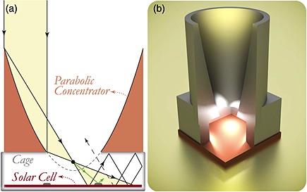
(a) Schematic illustration of the external light trap. By concentration, light is funneled through a small aperture and is trapped. Also shown in green is the reflection from a metallic reflective front contact. (b) A rendered 3D‐model of the light trap. The front quarter of the light trap is removed for visibility. A concentrator is placed on top of a square cage with the solar cell at the bottom (cell area shown in red). Most of the reflected light from the solar cell is recycled within the cage.
The external light trap reduces the need for internal light trapping schemes and anti‐reflection coatings that interfere with the electrical performance of the cell 25, 26, 27. An external light trap circumvents the electro‐optical dilemmas, because it allows one to focus mainly on the electrical performance of the cell. The light trap targets three major optical loss mechanisms present in all solar cells: (i) reflection at the cell at its front surface, metal fingers, busbars, and the reflective area between the solar cells; (ii) incomplete absorption, mainly at long wavelengths (λ); and (iii) photons emittedby radiative recombination. For most solar cells, like c‐Si, combating the losses due to reflection and poor absorption is most rewarding. Currently, the recycling of radiatively emitted photons is mainly interesting for gallium arsenide (GaAs) cells due to its relatively high external radiative efficiency 28, 29, 30, 31. Another benefit of the introduced concept is that it can help concentrated photovoltaics by reducing the heat load of the cell compared with conventional concentrated photovoltaics.
Internal light trapping schemes theoretically result in a path length enhancement of maximally 2n 2× the double cell pass 32. Therefore, external light trapping is of special interest for low refractive index (n ∼ 2) materials, such as organic and perovskite solar cells, because this method is independent of the refractive index.
The top of the external light trap is a compound parabolic concentrator (CPC). CPCs are generally applied for concentrated photovoltaics and solar thermal applications. There are basically three different categories of CPCs: macroscopic‐sized, millimeter‐sized, and micrometer‐sized concentrators. Macroscopic CPCs are commonly used in evacuated tube collectors and solar thermal applications 33, 34, 35. Millimeter‐sized CPCs were proposed to benefit from the relatively low Joule losses of small solar cells 36 and to realize a low‐cost, flat plate‐like concentrated photovoltaic module 37, 38, 39, while others fabricated micro‐sized CPCs using two‐photon lithography 23, 24.
We investigate the performance of the external light trap using a millimeter‐scaled 3D‐printed CPC placed on top of a 1.2 μm thick superstrate hydrogenated nanocrystalline silicon (nc‐Si:H) cell. The usage of the light trap is certainly not restricted to nc‐Si:H cells. This work opens a new domain of solar cell development in which no electro‐optical compromises are needed, leaving more space to focus on the electrical performance of the solar cell.
2. Optical Model for External Light Trapping
Thermodynamics forbids the concept of a one‐way mirror that would allow thermal heat to radiate unidirectionally from a cold to a hot body, because this violates the second law of thermodynamics 40. The external light trap seems to violate this law because light can travel unhindered from the sun to the solar cell, while most radiation originating from the solar cell is retro‐reflected by the trap. However, the trap also restricts the solid angle of light that is accepted, which enables an equivalent restriction of the escape area of the light confined in the trap 41. Therefore, the angular étendue restriction by the CPC enables efficient retro‐reflection of the light that did not escape through the aperture. Because the étendue restriction of radiatively emitted and accepted photons is identical, the external light trap does not violate thermodynamics.
For the external light trap, an absorption gain by light trapping is obtained upon placement of a cage between the CPC and the cell. The spacing of the cage enables sufficient divergence of the light beam, such that it does not escape through the aperture after the first reflection. The trap not only restricts the angular cone of acceptance, but also imposes an equivalent restriction for the trapped light: the light reflected by the solar cell outside this acceptance étendue is retro‐reflected. Because of this equivalency, the probability of photons to escape from the trap, P(escape), is in first order inversely proportional to the concentration factor (C).
| (1) |
where θ acceptance is the half angle of the acceptance cone of the concentrator 41. This reciprocity dictates that the restriction of the escape area within the light trap is inversely correlated to the angular acceptance restriction outside the trap, which is similar to rugate filters 29, 42, 43.
The restriction of the escape probability of photons increases the absorptance in the solar cell. In general, the intrinsic efficiency limit increases when the cell thickness is reduced while the absorptance stays constant 18. The improved energy conversion efficiency limit is possible because thin solar cells have effectively less recombination and thereby a relatively high open circuit voltage. This is illustrated by c‐Si solar cells. Because of the thickness‐related Auger and Shockley–Reed–Hall recombination, the maximum possible efficiency of ideally thin (3 μm) c‐Si cells under maximum angular restriction is 33.4% and thus significantly higher than 29.5% of a thick solar cell without angular restriction 18, 44, 45.
To explain the effectiveness of external light trapping, we introduce the following optical model. For simplicity, we first consider a hypothetical case in which light is completely diffused and homogenized inside the cage (or cavity). This condition can be realized by integrating a diffuser layer or white paint in the cage. Furthermore, we assume that the solar cell response does not depend on the angle of incidence of the light. Once a photon enters the cage and is reflected by the cell, the probability to escape via the aperture is in first order given by the following area ratio 41
In the low absorbing limit, the photons thereby traverse the cell statistically C times as much as a bare cell. The statistical‐averaged path length enhancement factor due to external light trapping (Πext, low absorbing) is roughly equal to the area ratio
| (2) |
where A CPC, A aperture, and A cell are, respectively, the area of the CPC opening, the CPC bottom aperture, and the illuminated cell area 33, 41. As A CPC was made equal to A cell, there is no effective enhancement due to concentration and we thus only investigate light trapping. In the low absorbing limit, the value of Πext of an angular restrictor is thus equivalent to C 41.
The optical model that we used includes the losses originating from the CPC, cage, and cell. Initially, a fraction T c is transmitted by the CPC and penetrates into the solar cell. A fraction T c A sc is absorbed. Most of the reflected light (R sc=T c(1 − A sc)) does not escape but is instead retro‐reflected by the top of the cage with reflectivity R cage. For homogeneously distributed light, a fraction C −1 escapes from the trap and (1 − C −1)R cage is reflected backwards by the cage. The cage absorbs a small fraction (1 − C −1)A cage. This process continues infinitely and the absorption accumulates. The total absorptance (A T) is thus given by
The sum of this geometric series is given by
| (3) |
All parameters, except C, are wavelength dependent.
Figure 2 shows the total absorptance for the cell with trap as a function of the bare cell absorptance for four light trapping cases. For a higher concentration factor, the escape probability is lower, and thereby, the total absorptance is higher. The quality of the CPC is more important for cells with a high absorptance as the optical loss in the CPC has to be compensated by light trapping. Low values of Πext (2 − 10×) do already have a significant impact on the absorptance. For example, for Πext=10×, a cell with an absorptance of just 20% will be enhanced to 60% by the light trap. When Πext increases, the total absorptance in the cell converges toward the transmittance of the CPC.
Figure 2.
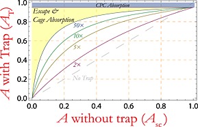
Absorptance enhancement by external light trapping. The four path length enhancement cases indicate the cell absorptance with light trap (A T) as a function of the bare cell absorptance (A sc) at the indicated concentration factors . T c is set to 95% and R cage to 95%.
It is of interest to compare internal and (concentrator based) external light trapping to identify the optimal method and to investigate how both trapping mechanisms can be combined. Internal light trapping is realized by scattering and total internal reflection within the cell. At low absorptivity, this results in a maximum theoretical path length enhancement factor of Πint=2n 2× with respect to a double cell pass 32, 46. For silicon cells, this corresponds to a factor of ∼2·3.52=24.5×. However, in practice, only broadband path length enhancement factors up to ~10× are realized 47.
For a perfect light trap, the external path length enhancement (Πext) is in the low absorbing limit equal to C (Eq. (2)). However, as a consequence of the non‐zero absorptance values, Πext ranges from 1× to 6×. From the experimental data, the effective path length enhancement factor can be derived using (Supporting Information)
| (4) |
The external light trap thus results in a path length enhancement of Πext, which is equivalent to an effective thickness of z eff=Πext·z, with z the solar cell thickness. Alternatively, one can consider the net effect of light trapping as an effective absorption coefficient (α) enhancement from α to Πext·α.
The total path length enhancement (Πtotal) is determined by the product of the internal and external path length enhancement factors, Πtotal=Πint·Πext, and thus,
| (5) |
where θ acceptance is the half angle of the acceptance cone 18. As θ sun is only ∼0.266°, this translates to a remarkable maximum path length enhancement factor in the order of for direct sunlight. The theoretically maximum contribution to the total path length enhancement from external light trapping is thus considerably higher than that of internal light trapping.
3. Design and Fabrication of the External Light Trap
After introducing the theoretical framework of the efficiency enhancing potential of the external light trap, we address its design and fabrication. A cross section of the fabricated light trap is illustrated in Figure 3(a). The CPC is designed in such a way that the angle of incidence at the cell at its front surface is below the Brewster angle of glass. This design prevents undesirably large Fresnel reflectance at large incidence angles; see Supporting Information. The optimization of the concentration factor of the light trap is primarily a trade‐off between the negative effects of design inaccuracies on the CPC transmission at high C and the improved absorptance due to path length enhancement at high C. It was found that, with the used 3D print technique and CPC size, it is technically challenging to realize high transmittance for concentration factors with C > 10×. This is mainly due to the need for higher accuracy with increase of C. Small deviations from the intended optical path will increasingly result in rejection of the light when the diameter of the exit aperture is reduced. Low concentration factors (C ~2 − 10×) are already sufficient to make a significant absorptance change. In this study, we therefore used a CPC with a geometrical concentration factor of C = 6, which experimentally showed both high transmittance and a descent absorption enhancement.
Figure 3.
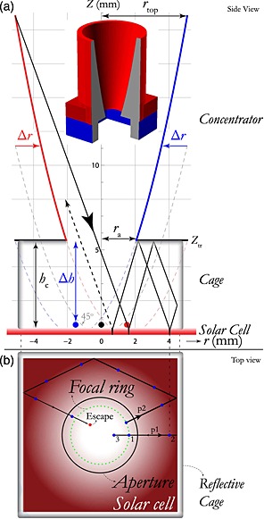
(a) A vertical cross section through the symmetry axis of the light trap. The compound parabolic concentrator (CPC) is rotationally symmetric, the cage is a cuboid. The light impacting the left side of the CPC is focused on the right red focal point and vice versa for blue. The inset shows a 3D model of the design: a circular CPC is placed directly on top of the square cage. (b) Top view of the square cage. Because of the rotational symmetry of the CPC, the focal points form a focal ring (indicated in green). Two horizontal projections of different light paths are shown. The blue dots indicate the spots where the light is reflected by the solar cell. Path p1 corresponds with that shown in Figure 3(a). Light following path p2 travels a longer distance and thus hits the cell more often compared with p1. The distance between the spots depends on the polar angle with the z axis. This in turn depends on the radial location where the initial beam hits the paraboloid.
One can engineer the light trap such that the path length enhancement for specular reflected light in the cage is even higher than the model, which is based on homogeneously distributed of light, would predict. The intensity (I) in the cell drops in first order exponentially according the Beer–Lambert law, I = I 0·e −α·l, with l the distance traveled through the cell. Once the trap is applied, the power escaping through the aperture is related to the exponential intensity decay with the number of cell passes: I escape=I 0·A #cell passes. The external light trap exploits this exponential decay as the specularly reflected light cannot escape from the trap in the first recycle events, because the light initially only propagates radially outwards; see Figure 3(b). This opportunity to postpone the first escape occurrence is an advantage over internal trapping schemes. This escape postponement cannot be obtained when the cell reflects the light diffusely. The largest path length enhancement is therefore expected for a flat, specular reflective cell, combined with a specular reflective cage. An additional advantage of a flat cell design is the superior electrical quality 15.
The light trap is 3D printed from acrylonitrile butadiene styrene using an Ultimaker 48. The use of acrylonitrile butadiene styrene (ABS) allows the prints to be vapor smoothened by exposure to a saturated acetone vapor; see Figure 4(a) and the Supporting Information. After smoothening, the cage and the CPC were silver coated, resulting in focusing of sunlight, as can be seen in Figure 4(b). Figure 4(c) shows the square cage and the circular concentrator that are stacked to form the light trap. The opening area of both the CPC and the cage is 81mm2. We used a square cage to match the usual shape of the solar cell. Moreover, the square cage design is an interesting candidate for large area module integration. By arranging multiple square cages into a square array, a large area can be efficiently covered by light traps 49. Some undesired unevenness of the parabolic shape can be observed by eye from the small distortion in the projected image inside of the CPC; see Figure 4(d). The formation of wrinkles might be prevented by using a more accurate fused deposition modeling printer and by improving the acetone treatment. As an alternative, one could use a different 3D printer, such as a stereolithography printer (based on optical curing of a resin).
Figure 4.
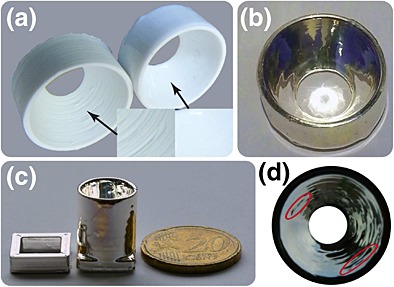
(a) A 3D‐printed compound parabolic concentrator (CPC) before and after chemical smoothening, the insets show the enlarged surface. (b) The silver‐coated CPC with a focal ring of sunlight at the center. (c) The separated cage and CPC that can be combined to an external light trap. (d) View of the CPC from the entrance side, showing the reflection in the parabolic curve. Two wrinkles in the concentrator are encircled in red.
The finished light trap was placed on top of a flat, square thin‐film nc‐Si:H solar cell prepared in superstrate configuration; see Figure 5. The fabrication of the solar cell is described in the Supporting Information. The light trap changes the angle of incidence to non‐normal angles. According to Snell's law, the path length thereby increases (relatively) more in the low refractive index ZnO than in the high index Si. This results in a relative increase of the parasitic losses.
Figure 5.
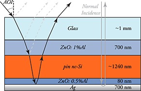
Illustration of the design of the hydrogenated nanocrystalline solar cell. The arrows indicate a light trace. Some interface reflections are shown in gray.
Depending on the exact geometry of the light trap, the illumination of the cell can become inhomogeneous, which negatively affects the cell performance 50, 51. We describe this potential issue and some solutions in more detail in the Supporting Information.
4. Results and Discussion
The square cage was placed on top of the square solar cell and used as a mask to determine the current density versus voltage (J–V) characteristics of the bare solar cell. Subsequently, the CPC (with equal opening area) is placed on top of the cage to determine the opto‐electrical improvement by the external light trapping. Figure 6 shows the J–V characteristics at AM1.5G illumination of the bare (masked) solar cell and the cell with the external light trap (cage and concentrator). Because of the light trapping, the short circuit current density (J sc) and the current at the maximum power point (J mpp) improved by 14% and 15%, respectively. No significant change in the fill factor and open circuit voltage (V oc) was measured. To understand the origin of this enhancement, we determined the internal quantum efficiency (IQE), absorptance, and external quantum efficiency (EQE).
Figure 6.
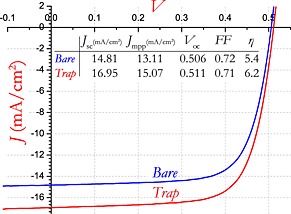
J–V characteristic of the bare solar cell (with the cage used as a mask) and the solar cell with the external light trap.
The IQE of the bare cell was determined by measuring the absorptivity (A sc=1 − R sc) and the EQE; see Figure 7. For short wavelengths (λ<400 nm), the absorptance of the bare cell is high (~80–90%). The relatively high parasitic absorptance in the ZnO front contact and the (not photovoltaically active) p‐layer results in a low EQE and IQE. This implies that there is only a small potential for improvement (~10% to 20% relative) in this short wavelength regime. For wavelengths around 600 nm, the reflectance is 10% to 40%, while at the same time, the IQE is high. This provides significant room for improvement by external light trapping. For longer wavelengths (λ>700 nm) there is 40–60% reflection. With further increase of the wavelength, the absorptance in the nc‐Si reduces compared with the parasitic absorptance, and therefore, the IQE drops to zero. In the first order, the achievable EQE improvement is given by EQE ↑=R sc·IQE. Thus, the light trap mainly improves the response when both R sc and IQE are high, this is the case for ~400<λ<~900 nm. The observed optical interference patterns are mainly due to the Fabry–Pérot modes in the 1.2 μm thick Si layer.
Figure 7.
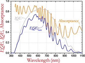
Plot of the total absorptance, the EQE, and the derived IQE of the bare solar cell.
Figure 8 shows the EQE of the bare cell (EQE bare), the EQE of the cell with trap (EQE trap), and the EQE as calculated using the model (EQE model). There is a significant EQE improvement from EQE bare to EQE trap over the full spectrum. At short wavelengths, the improvement is due to retro‐reflection of light that is reflected at the front interface of the cell. Thereby, the net reflectance is reduced somewhat similar to that of an anti‐reflection coating. For long wavelengths, there is also retro‐reflection of light that passed the solar cell but was not absorbed. The enhancement demonstrates that indeed the external light trap effectively prolongs the optical path length in the cell.
Figure 8.
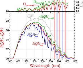
Plot of the EQE bare and internal quantum efficiency (IQE) of the bare solar cell (without light trap). Also shown is the external quantum efficiency (EQE) of the solar cell with external light trap (EQE trap) and the expected EQE of the cell with light trap based on the optical model (EQE model). The external path length enhancement factor (top of figure) shows that there is an improved optical path length for all wavelengths. As expected, there is an anti‐correlation of blackΠext with the interference pattern as indicated by the red and blue bars.
The curve of EQE trap is smoother than that of EQE bare, which can be explained by two effects. First, as the EQE trap converges toward the IQE, the interference fringes are reduced. Second, the trap offers a range of non‐normal angles of incidence resulting in a range of different overlapping Fabry–Pérot resonances with a more constant average. A distribution of the path length in the cell with a small dispersion of just a few percent significantly smoothens the absorptance and EQE.
From the introduced model (Eq. (3)), the achievable EQE was calculated using EQE bare and the IQE; see EQE model in Figure 8. The following parameter values were used: T c=0.95, C = 6, and R cg=0.93. The overall trend of EQE model corresponds well with the measured EQE trap. There is excellent agreement at short wavelengths between the model and the experimental data. The observed decrease of the interference fringes of EQE trap corresponds with the trend of the model. Although the EQE trap approaches EQE model, there is a discrepancy that is attributed to several losses that were not included in the model. (i) The glass between the light trap and the solar cell enables some light to escape sideways. (ii) The printed cage and the CPC are not perfectly smooth, resulting in unwanted parasitic absorption and reflection in unintended directions. (iii) Imperfect interconnection of the cell, the 3D‐printed cage, and the CPC causes small cavities (around a few hundred μm) that give rise to a small escape loss (estimated to be a few percent). (iv) The wavelength dependence of the parameters was not taken into account. Finally, as IQE trap cannot be determined experimentally, we assumed for the model that IQE bare is equal to IQE trap. Based on the model, the J sc of the cell with light trap could be ideally 19.9 mA/cm2. Therefore, by reducing the indicated loss mechanisms, one could gain another 2.9 mA/cm2.
The realized and expected external path length enhancements (Πexperimental and Πmodel) were calculated by evaluating Eq. (4) on the implied absorptivity as described in the Supporting Information; see top of Figure 8. The external path length enhancement ranges from 1.5 to 2.5× in the long wavelength regime, where light trapping is mostly needed. The pattern of Πexperimental agrees with the expected Πmodel.
The path length enhancement is anti‐correlated to the EQE, as can be seen from the vertical red and blue background bars in Figure 8. This agrees with the optical model, which indicates that the achievable path length enhancement is roughly inversely related to the bare cell absorptance (Supporting Information). Besides that, the before mentioned smoothening of EQE trap also results in an anti‐correlation of the Πext and EQE data as the interference minima of the EQE trap relatively increase, while the maxima relatively decrease.
A high‐quality external light trap with a moderate (e.g., ~10×) path length enhancement factor and low parasitic absorption losses results in an EQE trap just below the IQE. In the design process of solar cells that are to be combined with a light trap, one has to optimize the IQE. This can be carried out by preventing undesirable parasitic absorption, for example, in the back reflector 52.
The question now arises how external light trapping differs from conventional light concentration. Concentrators are commonly used to concentrate light directly on a solar cell to profit from reduced, relative expensive, cell usage and the higher open circuit voltage. For a cell under concentrated light (without internal light trapping), light traverses the cell just back and forth, after which the non‐absorbed light escapes through the front surface. However, for a cell with an external light trap, the light is forced to traverse the cell many times, which allows the use of thinner and untextured cells, resulting in less bulk and surface recombination.
Several improvements for external light trapping can be envisaged. The (individual) external light trap can be scaled to a larger area by designing a CPC array as was shown recently 49. Large trapping arrays can be made at low cost from ABS plastic (which we also used for the 3D printing) by injection molding. It has been shown that the thickness of CPC arrays can be scaled down to the micrometer range, which benefits module integration 23, 24. The need of sun tracking can be eliminated by matching the acceptance cone of the CPC to the path of the sun. Finally, the positive effects of an enhanced V oc due to light concentration can be combined with light trapping. For example, when a CPC with a concentration factor of 6× is combined with a solar cell with a smaller area of A cell=A CPC/2, there is both concentration (effectively 2×) and light trapping (Πext=3×). This also enables mitigation of the high shading losses of the metal grid in concentrator cells of 10–20% 47. Moreover, the reduced flux will help to mitigate heat problems at cell level compared with full concentration.
The design of the cage is another aspect of the light trap that can be improved. It has been shown that an oblate hemi‐ellipsoidal cavity with a specular reflective coating would be an interesting candidate 30, 41, 53, 54, 55. In this design, the solar cell is located in between the focal circle of the ellipsoid, and thereby, all the light reflecting from the solar cell is reflected backwards to the cell in just one reflection. This enables efficient recycling as it keeps the parasitic absorptance by the cage low.
For isotropically distributed incident diffuse light, a fraction 1/C is transmitted by the parabolic concentrator 34. Therefore, the use of low concentration factors (C~2‐10×) enables transmitting 10–50% of the diffuse light. There is an inevitable trade‐off between loss of diffuse light and reduced escape probability (within the light trap) with increase of C. Further research should be performed to determine an optimal concentration factor. Alternatively, it is worthwhile to model and realize an earlier proposed concept in which both the diffuse and direct components are harvested by geometric separation 56.
5. Conclusions
We used a combination of a 3D‐printed parabolic concentrator and a light cage to demonstrate external light trapping for a thin‐film nc‐Si:H solar cell. We showed a 15% enhancement of the energy conversion efficiency in this cell with respect to the same cell without an external light trap. The external light trap recycled both the unwanted reflection from the front side of the cell and enhanced the poor absorptance in the long wavelength regime. The measured absorptance enhancement at short wavelengths demonstrates the anti‐reflection effect of the trap. We introduced an absorptance model for external light trapping and showed good correspondence with the experimental data. As a result of light trapping, a path length enhancement factor up to 2.5× was observed. Several optical loss mechanisms were found and described that can be targeted in future research to obtain better trapping than this initial result. For further research, we recommend to focus on the accuracy and the related transmittance of the CPC.
The parasitic absorption losses of this first prototype of the CPC are more than compensated by the gain in the cell absorptance. We showed that the efficiency improvement is caused by an unprecedented broadband absorption enhancement by the external light trap 57, 58, 59, which is universally applicable to all solar cell technologies. Higher gains can be expected upon further optimization of the reflections in the trapping system. Reducing the cell thickness combined with the external light trap is a promising way for further efficiency improvement.
The trap enables decoupling of the optical and electric optimization, which yields new perspectives for the design of solar cells. In the current solar cell market, revolutionary light trapping architectures are needed to obtain higher efficiencies. The demonstrated 3D‐printed external light trap is an attractive candidate to accomplish this target.
Supporting information
Supporting Info Item
Supporting Info Item
Acknowledgements
The authors acknowledge the insightful discussions with and help of J. van de Groep, J.K. Rath, T. van der Beek, U. Rau, K. Bittkau, and E.A.P. Marcus. The authors are grateful for the technical assistance from N.J. Bakker, T. van den Driesschen, D. Lamers, and H. Zeijlemaker. We thank T. Merdzhanova, D. Weigand, and U. Gerhards for the fabrication of the solar cell. The authors are grateful to the Amsterdam Nanocenter at the FOM Institute AMOLF for the use of the clean room and to ECN for using their characterization facilities. This work was supported by the NanoNextNL, a micro and nanotechnology consortium of the Government of the Netherlands and 130 partners. We also acknowledge the funding provided by the Marie Curie Career Integration Grant and the Postdoc‐Program of the German Academic Exchange Service (DAAD). The collaboration between the Forschungszentrum Jülich GmbH (IEK5‐Photovoltaik), Utrecht University, ECN, and Eindhoven University of Technology was initiated within the Solliance Research Program. We acknowledge the makers of OpenSCAD for freely distributing their software 60.
Dijk, L. , Paetzold, U. W. , Blab, G. A. , Schropp, R. E. I. , and di Vece, M. (2016) 3D‐printed external light trap for solar cells. Prog. Photovolt: Res. Appl., 24: 623–633. doi: 10.1002/pip.2702.
References
- 1. Mokkapati S, Catchpole KR. Nanophotonic light trapping in solar cells. Journal of Applied Physics. 2012; 112: 101101. [Google Scholar]
- 2. Polman A, Atwater HA. Photonic design principles for ultrahigh‐efficiency photovoltaics. Nature Materials. 2012; 11: 174–177. [DOI] [PubMed] [Google Scholar]
- 3. Rau U, Kirchartz T. On the thermodynamics of light trapping in solar cells. Nature Materials. 2014; 13: 103–104. [DOI] [PubMed] [Google Scholar]
- 4. Rau U, Paetzold UW, Kirchartz T. Thermodynamics of light management in photovoltaic devices. Physical Review B. 2014; 90(3): 035211. [Google Scholar]
- 5. Sun CH, Jiang P, Jiang B. Broadband moth‐eye antireflection coatings on silicon. Applied Physics Letters. 2008; 92(6): 061112. [Google Scholar]
- 6. Matsui T, Tsukiji M, Saika H, Toyama T, Okamoto H. Influence of substrate texture on microstructure and photovoltaic performances of thin film polycrystalline silicon solar cells. Journal of Non‐Crystalline Solids. 2002; 299: 1152–1156. [Google Scholar]
- 7. Schropp REI, Rath JK, Li H. Growth mechanism of nanocrystalline silicon at the phase transition and its application in thin film solar cells. Journal of Crystal Growth. 2009; 311: 760–764. [Google Scholar]
- 8. Python M, Dominé D, Söderström T, Meillaud F, Ballif C. Microcrystalline silicon solar cells: effect of substrate temperature on cracks and their role in post‐oxidation. Progress in Photovoltaics: Research and Applications. 2010; 18: 491–499. [Google Scholar]
- 9. Paetzold UW, Smeets M, Meier M, Bittkau K, Merdzhanova T, Smirnov V, Michaelis D, Waechter C, Carius R, Rau U. Disorder improves nanophotonic light trapping in thin‐film solar cells. Applied Physics Letters. 2014; 104: 131102. [Google Scholar]
- 10. Springer J, Poruba A, Müllerova L, Vanecek M, Kluth O, Rech B. Absorption loss at nanorough silver back reflector of thin‐film silicon solar cells. Journal of Applied Physics. 2004; 95: 1427–1429. [Google Scholar]
- 11. Haug FJ, Söderström T, Cubero O, Terrazzoni‐Daudrix V, Ballif C. Plasmonic absorption in textured silver back reflectors of thin film solar cells. Journal of Applied Physics. 2008; 104: 064509. [Google Scholar]
- 12. Moulin E, Paetzold UW, Kirchhoff J, Bauer A, Carius R. Study of detached back reflector designs for thin‐film silicon solar cells. physica status solidi (RRL) ‐ Rapid Research Letters. 2012; 6: 65–67. [Google Scholar]
- 13. Spinelli P, Polman A. Prospects of near‐field plasmonic absorption enhancement in semiconductor materials using embedded ag nanoparticles. Optics Express. 2012; 20: A641–A654. [DOI] [PubMed] [Google Scholar]
- 14. van Lare M, Lenzmann F, Polman A. Dielectric back scattering patterns for light trapping in thin‐film Si solar cells. Optics Express. 2013; 21: 20738–20746. [DOI] [PubMed] [Google Scholar]
- 15. Sai H, Kanamori Y, Kondo M. Flattened light‐scattering substrate in thin film silicon solar cells for improved infrared response. Applied Physics Letters. 2011; 98: 113502. [Google Scholar]
- 16. Biswas R, Xu C. Nano‐crystalline silicon solar cell architecture with absorption at the classical 4n 2 limit. Optics Express. 2011; 19: A664–A672. [DOI] [PubMed] [Google Scholar]
- 17. Wang KX, Yu Z, Liu V, Cui Y, Fan S. Absorption enhancement in ultrathin crystalline silicon solar cells with antireflection and light‐trapping nanocone gratings. Nano Letters. 2012; 12: 1616–1619. [DOI] [PubMed] [Google Scholar]
- 18. Campbell P, Green MA. The limiting efficiency of silicon solar cells under concentrated sunlight. IEEE Transactions on Electron Devices. 1986; 33: 234–239. [Google Scholar]
- 19. Winston R. Principles of solar concentrators of a novel design. Solar Energy. 1974; 16: 89–95. [Google Scholar]
- 20. Gaspare M. High yielding solar modulus for the transformation, on photovoltaic cells, of a substantially monochromatic radiation in electric energy, 1986. EP Patent App. EP19,840,830,013.
- 21. Goetzberger A, Goldschmidt JC, Peters M. Patent, photovoltaic device and use thereof, 2012. WO2011098212.
- 22. Peumans P, Bulović V, Forrest SR. Efficient photon harvesting at high optical intensities in ultrathin organic double‐heterostructure photovoltaic diodes. Applied Physics Letters. 2000; 76: 2650–2652. [Google Scholar]
- 23. Atwater JH, Spinelli P, Kosten E, Parsons J, Van Lare C, Van de Groep J, Garcia de Abajo J, Polman Albert, Atwater HarryA. Microphotonic parabolic light directors fabricated by two‐photon lithography. Applied Physics Letters. 2011; 99: 151113–151113. [Google Scholar]
- 24. Yan W, Hossain MM, Gu Min. High light‐directing micrometer‐sized parabolic mirror arrays. Optics Letters. 2013; 38: 3177–3180. [DOI] [PubMed] [Google Scholar]
- 25. Spinelli P, Macco B, Verschuuren MA, Kessels WMM, Polman A. Al2O3/TiO2 nano‐pattern antireflection coating with ultralow surface recombination. Applied Physics Letters. 2013; 102: 233902. [Google Scholar]
- 26. Luque A, Hegedus S. Handbook of Photovoltaic Science and Engineering. John Wiley & Sons, 2011. [Google Scholar]
- 27. Zhao J, Wang A, Green MA, Ferrazza F. 19.8% efficient "honeycomb" textured multicrystalline and 24.4% monocrystalline silicon solar cells. Applied Physics Letters. 1998; 73: 1991–1993. [Google Scholar]
- 28. Kosten ED, Atwater JH, Parsons J, Polman A, Atwater HA. Highly efficient GaAs solar cells by limiting light emission angle. Light: Science & Applications. 2013; 2: e45. [Google Scholar]
- 29. Kosten ED, Kayes BM, Atwater HA. Experimental demonstration of enhanced photon recycling in angle‐restricted gaas solar cells. Energy & Environmental Science. 2014; 7: 1907–1912. [Google Scholar]
- 30. Braun A, Katz EA, Feuermann D, Kayes BM, Gordon JM. Photovoltaic performance enhancement by external recycling of photon emission. Energy & Environmental Science. 2013; 6: 1499–1503. [Google Scholar]
- 31. Green MA. Radiative efficiency of state‐of‐the‐art photovoltaic cells. Progress in Photovoltaics: Research and Applications. 2012; 20: 472–476. [Google Scholar]
- 32. Yablonovitch E. Statistical ray optics. Journal of the Optical Society of America. 1982; 72: 899–907. [Google Scholar]
- 33. Winston R, Miñano JC, Benítez P. Nonimaging Optics, Electronics & Electrical Elsevier Academic Press: Burlington, MA 01803, USA, 2005. [Google Scholar]
- 34. Rabl A, O'gallagher J, Winston R. Design and test of non‐evacuated solar collectors with compound parabolic concentrators. Solar Energy. 1980; 25(4): 335–351. [Google Scholar]
- 35. Solargenix energy. http://www.solargenix.com/.
- 36. Paire M, Lombez L, Péré‐Laperne N, Collin S, Pelouard J‐L, Lincot D, Guillemoles J‐F. Microscale solar cells for high concentration on polycrystalline Cu (In, Ga) Se2 thin films. Applied Physics Letters. 2011; 98(26): 264102. [Google Scholar]
- 37. Jared BH, Saavedra MP, Anderson BJ, Goeke RS, Sweatt WC, Nielson GN, Okandan M, Elisberg B, Snively D, Duncan J, . et al. Micro‐concentrators for a microsystems‐enabled photovoltaic system. Optics express. 2014; 22(102): A521–A527. [DOI] [PubMed] [Google Scholar]
- 38. Gu T, Agrawal G, Vessey A, Sweatt WC, Jared BH, Cruz‐Campa JL, Goeke R, Miller WK, Zamora DL, Langlois E, Okandan M, Nielson GN, Haney MW. 2015. Micro‐concentrator module for microsystems‐enabled photovoltaics: optical performance characterization, modeling and analysis In The proceedings of the 42nd IEEE PVSC, New Orleans, LA. [Google Scholar]
- 39. Jutteau S, Paire M, Lombez L, Guillemoles J‐F. 2015. Micro solar concentrators: design and fabrication for microcells arrays In The proceedings of the 42nd IEEE PVSC, New Orleans, LA. [Google Scholar]
- 40. Würfel P, Würfel U. Physics of Solar Cells: From Basic Principles to Advanced Concepts. John Wiley & Sons: Weinheim, Germany, 2009. [Google Scholar]
- 41. Luque A, Miñano JC. Optical aspects in photovoltaic energy conversion. Solar Cells. 1991; 31: 237–258. [Google Scholar]
- 42. Ulbrich C, Peters M, Bläsi B, Kirchartz T, Gerber A, Rau U. Enhanced light trapping in thin‐film solar cells by a directionally selective filter. Optics Express. 2010; 18: A133–A138. [DOI] [PubMed] [Google Scholar]
- 43. Höhn O, Kraus T, Bauhuis G, Schwarz UT, Bläsi B. Maximal power output by solar cells with angular confinement. Optics Express. 2014; 22(103): A715–A722. [DOI] [PubMed] [Google Scholar]
- 44. Kosten ED, Newman BK, Lloyd JV, Polman A, Atwater H. Limiting light escape angle in silicon photovoltaics: ideal and realistic cells. IEEE Journal of Photovoltaics. 2015; 5(1): 61–69. [Google Scholar]
- 45. Shockley W, Queisser HJ. Detailed balance limit of efficiency of p–n junction solar cells. Journal of Applied Physics. 1960; 32: 510–519. [Google Scholar]
- 46. Green MA. Lambertian light trapping in textured solar cells and light‐emitting diodes: analytical solutions. Progress in Photovoltaics: Research and Applications. 2002; 10: 235–241. [Google Scholar]
- 47. Nelson J. The Physics of Solar Cells. World Scientific, 2003. [Google Scholar]
- 48. Ultimaker homepage. www.ultimaker.com.
- 49. van Dijk L, Marcus EAP, Oostra AJ, Schropp REI, Di Vece M. 3D‐printed concentrator arrays for external light trapping on thin film solar cells. Solar Energy Materials and Solar Cells. 2015; 139: 19–26. [Google Scholar]
- 50. Luque A, Sala G, Arboiro JC. Electric and thermal model for non‐uniformly illuminated concentration cells. Solar Energy Materials and Solar Cells. 1998; 51(3): 269–290. [Google Scholar]
- 51. Gordon JM, Feuermann D, Mashaal H. Micro‐optical designs for angular confinement in solar cells. Journal of Photonics for Energy. 2015; 5(1): 055599–055599. [Google Scholar]
- 52. Holman ZC, De Wolf S, Ballif C. Improving metal reflectors by suppressing surface plasmon polaritons: a priori calculation of the internal reflectance of a solar cell. Light: Science & Applications. 2013; 2: e106. [Google Scholar]
- 53. Gordon JM, Feuermann D, Huleihil M, Katz EA. New optical systems for the solar generation of nanomaterials. In Optical Science and Technology, SPIE's 48th Annual Meeting, 2004; 99–108.
- 54. Weinstein L, Kraemer D, McEnaney K, Chen G. Optical cavity for improved performance of solar receivers in solar‐thermal systems. Solar Energy. 2014; 108: 69–79. [Google Scholar]
- 55. Weinstein LA, Hsu W‐C, Yerci S, Boriskina SV, Chen Gang. Enhanced absorption of thin‐film photovoltaic cells using an optical cavity. Journal of Optics. 2015; 17(5): 055901. [Google Scholar]
- 56. Tormen M, Inganäs O, Tvingstedt K, Zilio SD. Photovoltaic device with enhanced light harvesting, 2010. US Patent App. 12/601,798.
- 57. Tvingstedt K, Dal Zilio S, Inganäs O, Tormen M. Trapping light with micro lenses in thin film organic photovoltaic cells. Optics Express. 2008; 16: 21608–21615. [DOI] [PubMed] [Google Scholar]
- 58. Peters M, Ulbrich C, Goldschmidt JC, Fernandez J, Siefer G, Bläsi B. Directionally selective light trapping in a germanium solar cell. Optics Express. 2011; 19: A136–A145. [DOI] [PubMed] [Google Scholar]
- 59. Kim SJ, Margulis GY, Rim S‐B, Brongersma ML, McGehee MD, Peumans P. Geometric light trapping with a V‐trap for efficient organic solar cells. Optics Express. 2013; 21: A305–A312. [DOI] [PubMed] [Google Scholar]
- 60. Openscad, CAD software. www.openscad.org.
Associated Data
This section collects any data citations, data availability statements, or supplementary materials included in this article.
Supplementary Materials
Supporting Info Item
Supporting Info Item


