Abstract
Nano-structured CuO-Cu2O complex thin film-based perovskite solar cells were fabricated on an indium tin oxide (ITO)-coated glass and studied. Copper (Cu) thin films with a purity of 99.995 % were deposited on an ITO-coated glass by magnetron reactive sputtering. To optimize the properties of the nano-structured CuO-Cu2O complex thin films, the deposited Cu thin films were thermally oxidized at various temperatures from 300 to 400 °C. A CH3NH3PbI3 perovskite absorber was fabricated on top of CuO-Cu2O complex thin film by a one-step spin-coating process with a toluene washing treatment. Following optimization, the maximum power conversion efficiency (PCE) exceeded 8.1 %. Therefore, the low-cost, solution-processed, stable nano-structured CuO-Cu2O complex thin film can be used as an alternative hole transport layer (HTL) in industrially produced perovskite solar cells.
Keywords: Nano-structured, CuO-Cu2O complex-based, CH3NH3PbI3 perovskite
Background
Organic–inorganic hybrid perovskite (such as CH3NH3PbX3, X = I, Cl, Br) solar cells has attracted much attention because of its superior photovoltaic performance, including excellent light-harvesting ability and potential applications [1–6]. In previous reports, the high power conversion efficiency (PCE) of perovskite solar cells was achieved when a conducting polymer PEDOT:PSS thin film that was formed using TiO2 nano-particles that had been sintered at high temperature was used as the electron transport layer (ETL) (hole transport layer (HTL)) [7–9]. However, a trade-off must be between fabrication cost and device stability, impeding the development of commercialized solar cells. Inorganic p-type materials as hole transport media have the double advantage of excellent chemical stability and simplicity of preparation [10–12]. Along with some inorganic HTLs (copper iodide (CuI) [13], copper thiocyanate (CuSCN) [14–16], graphene oxide (GO) [17], nickel oxide (NiO) [18], cuprous oxide (Cu2O), and copper oxide (CuO) [19] have attracted substantial interest owing to their direct gaps of 1.9–2.2 eV[20–22], and these have been widely used as HTLs in solar cells. Cu2O and CuO thin films can be prepared by various methods, including reactive sputtering [23], electrochemical deposition [24–27], chemical dissolution [28–30], thermal oxidation [31], and successive ionic layer adsorption and reaction (SILAR) method [12, 32].
In this work, CuO-Cu2O complex thin films were prepared from thermally oxidized Cu thin films to form HTLs for use in perovskite solar cells. The structural, optical, and surface properties of CuO-Cu2O complex thin films were investigated to elucidate the performance of CuO-Cu2O complex thin film-based photovoltaics. The device with an optimized CuO-Cu2O complex thin film as the HTL exhibited superior photovoltaic performance, revealing that the CuO-Cu2O complex thin film is a potential inorganic HTL for use in perovskite solar cells.
Methods
Firstly, Cu layers were deposited on an indium tin oxide (ITO) glass substrate by RF magnetron reactive sputtering from Cu targets in gaseous argon (Ar) at a flow rate of 15 sccm and a stable working pressure of 3 × 10⁻³ Torr. The nano-structured CuO-Cu2O complex thin films were formed by thermally oxidizing Cu on ITO substrate at various annealing temperatures from 300 to 400 °C for 1 h in air, and these acted as HTLs. 1.25 M Pbl2 and 1.25 M methylammonium iodide (MAI) were dissolved in a cosolvent mixture of dimethyl sulfoxide (DMSO) and γ-butyrolactone (GBL) (vol. ratio = 1:1), and the resulting solution was used as the perovskite precursor solution. The CH3NH3PbI3 perovskite precursor was spin-coated on top of the nano-structured CuO-Cu2O complex/ITO/glass and underwent in situ non-polar solvent washing treatment [1–3] in a glove box that was filled with highly pure nitrogen. The CH3NH3PbI3 perovskite precursors were then coated onto the CuO-Cu2O complex/ITO/glass samples in two consecutive spin-coating steps at 1000 and 5000 rpm for 10 and 20 s, respectively. At 5000 rpm for 20 s, the wet spinning film was quenched by dropping 100 μl of anhydrous toluene onto it. After spin coating, the film was annealed at 100 °C for 5 min. Finally, C60, BCP, and the Ag electrode were sequentially deposited by thermal evaporation at a base pressure of 5 × 10⁻⁶ Pa. The thicknesses of C60, BCP, and Ag were 50, 5, and 100 nm, respectively. Figure 1a presents the steps in the preparation of CuO-Cu2O complex thin film-based perovskite solar cells. The C60 thin film, CH3NH3PbI3 perovskite thin film, and CuO-Cu2O complex thin film in the cell structure acted as the ETL, the active layer, and the HTL, respectively. A shadow mask firmly covered the sample to define an active area of 0.5 cm × 0.2 cm during C60/BCP/Ag deposition. Figure 1b shows the photo image of the shadow mask. Figure 1c schematically depicts the complete structure.
Fig. 1.
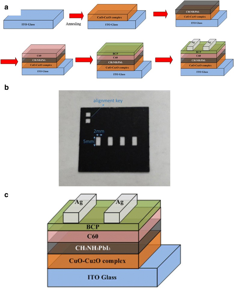
a Preparation of nano-structured CuO-Cu2O complex films, b photograph image of shadow mask, and c structure of device
The crystal characteristics of the CuO-Cu2O complex thin films were determined using an X-ray diffractometer (XRD) (D8, Bruker). Raman scattering spectroscopy was used to analyze the CuO-Cu2O complex thin films. A field-emission scanning electron microscope (FESEM) (LEO 1530) was used to observe the cross-section and surface morphology of the cells. The current density–voltage (J-V) characteristics were measured using a Keithley 2400 programmable source/meter unit under irradiation by a 1000 W xenon lamp. To evaluate the photovoltaic performance, the irradiation power density on the surface of the sample was calibrated as set to 1000 W/m2. Photoelectron emission measurement (manufactured by Riken Keiki, Model AC-2) was performed in the air and at room temperature.
Results and Discussion
Table 1 presents the Hall measurements of the CuO-Cu2O thin films. The increase in the carrier mobility at 250–300 °C could be attributed to an improvement in the crystallinity as well as a decrease in the carrier density because carrier mobility is generally affected by grain boundary scattering and by impurity scattering due to the native defects. However, as the annealing temperature increased to 400 °C, the mobility in the sample decreased from 33.5 to 17.9 cm2/Vs for owing to the decrease in the size of the grains caused by the phase transformation from Cu2O to CuO. As the thermal annealing temperature increased, the reduction of resistivity of the CuO-Cu2O complex films post-annealing may be attributed to both the carrier concentration and carrier mobility were decreased gradually, resulting in an increase in resistivity. The reduction of mobility is attributable to the transportation of carriers from one grain to another grain.
Table 1.
Hall measurements of CuO-Cu2O complex films
| Annealing temp. (°C) | Resistivity (Ω-cm) | Carrier concentration ×1017 (cm−3) | Mobility (cm2/V-s) |
|---|---|---|---|
| As-deposited | 2.1 | 2.9 | 10.3 |
| 300 | 1.5 | 2.1 | 19.3 |
| 350 | 2.0 | 9.2 | 33.5 |
| 400 | 9.7 | 3.6 | 17.9 |
Figure 2 plots the J-V curves for the CuO-Cu2O complex thin film-based perovskite solar cells under 100 mW/cm2 illumination (AM 1.5G). Tables 2 and 3 list the characteristic parameters of these devices. The PCE is improved from 3.15 to 7.32 % as the thermal oxidation temperature increases from 300 to 350 °C, mainly owing to the increase in the photo-generated carriers extracted and injected into the electrode caused by the carrier mobility and series resistance in the device, and then to result in the increase in the short-circuit current density (JSC). The PCE decreases from 7.32 to 6.43 % as the thermal oxidation temperature increased from 350 to 400 °C. As listed in Table 2, for the device annealing at 400 °C, the series resistance (Rs) increases and the shunt resistance (Rsh) decreases. The degradation of the performance may be attributed to the degradation of ITO electrode and leakage between CuO-Cu2O complex and perovskite layer. The PCE of CuO-Cu2O complex thin film-based perovskite solar cells is improved from 7.32 to 8.10 % as the thickness of CuO-Cu2O complex thin film increased from 30 to 60 nm. However, further increasing the thickness of the CuO-Cu2O complex thin film to 120 nm reduced the PCE from 8.10 to 5.20 % due to the series resistance effect in the cell, as listed in Table 3. According to the J-V curve and PCE value, the optimized thickness of the CuO-Cu2O complex thin film is 60 nm.
Fig. 2.
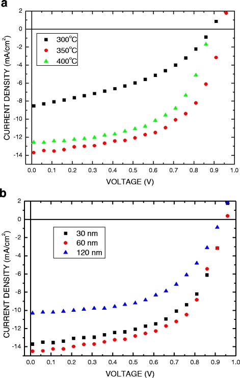
Current–voltage (J-V) characteristics of perovskite solar cell that was constructed using CuO-Cu2O complex thin film under simulated illumination with a light intensity of 100 mW/cm2 (AM 1.5). a Thermal oxidation temperatures. b The thicknesses of CuO-Cu2O complex thin film
Table 2.
Parameters of CuO-Cu2O complex thin film-based perovskite solar cells following thermal oxidation of the film at various temperatures
| Annealing temp. (°C) | VOC(V) | JSC(mA/cm2) | FF(%) | Eff(%) | Rs(Ω) | Rsh(Ω) |
|---|---|---|---|---|---|---|
| 300 | 0.88 | 8.56 | 41. 42 | 3.15 | 25.8 | 234 |
| 350 | 0.95 | 13.88 | 55.54 | 7.32 | 7.9 | 738 |
| 400 | 0.89 | 12.71 | 56.89 | 6.43 | 12.5 | 698 |
Table 3.
Parameters of CuO-Cu2O complex thin film-based perovskite solar cells with films of different thicknesses
| CuO-Cu2O complex thickness (nm) | VOC(V) | JSC(mA/cm2) | FF(%) | Eff(%) | Rs(Ω) | Rsh(Ω) |
|---|---|---|---|---|---|---|
| 30 | 0.95 | 13.88 | 55.54 | 7.32 | 12.9 | 410 |
| 60 | 0.96 | 14.40 | 58.61 | 8.10 | 10.3 | 789 |
| 120 | 0.93 | 10.28 | 54.45 | 5.20 | 21.9 | 338 |
In this study, the X-ray diffraction technique was used to elucidate the crystal characteristics of CuO-Cu2O complex thin films. To determine the relationship between thermal oxidation temperature and mechanism, the phase of the CuO-Cu2O complex thin films was identified. Figure 3 shows the XRD patterns of CuO-Cu2O complex thin films that were deposited on a glass substrate. XRD experimental results demonstrate that the crystalline phases of CuO and Cu2O were formed at different thermal oxidation temperatures. Diffraction peaks at 35.84° and 38.85° corresponded to the (−111) and (100) planes of the cubic-structured CuO, and diffraction peaks at 36.8° and 38.63° corresponded to the (111) and (200) planes of the cubic-structured Cu2O. A broad diffraction peak at 35.84° was obtained from the Cu/ITO/glass sample following thermal annealing at 350 °C. This peak may be attributed to a complex layer that comprised the (−111) plane of CuO and the (111) plane of Cu2O. The XRD patterns of Cu2O (CuO) gradually decrease (increase) as the thermal annealing temperature increased from 300 to 400 °C, indicating that the crystalline Cu2O is completely converted to crystalline CuO. The crystal domain size G was calculated according to the Scherrer’s equation: [33]
| 1 |
Fig. 3.
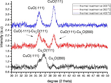
XRD diffractograms of CuO-Cu2O complex thin film following thermal oxidation at various temperatures
where G, λ, β, and θ denote the grain size, the X-ray wavelength, the full width at half maximum (FWHM) in radians, and the Bragg angle of CuO or Cu2O peak, respectively. The phase transformation from crystalline Cu2O to crystalline CuO reduces the crystal domain size from 31.83 to 29.39 nm, and thereby increases the carrier mobility of the CuO-Cu2O complex thin films, improving the carrier collection at the CH3NH3PbI3/CuO-CuO2 complex interface. However, the phase transformation reduces the grain size and surface roughness of the CuO-Cu2O complex thin films, as presented in Fig. 4, which presents FESEM images of the Cu layers that had undergone thermal oxidation at various annealing temperatures. More flat surface favors the coverage of the subsequently coated perovskite layer and C60 layer on the Cu-CuO2 complex thin films to form the continuous films and so improves the fill factor of the perovskite solar cells (Table 2). The image of the Cu layer that underwent thermal treatment at 350 °C reveals that the surface of the film consisted of small particles. The mean particle size was approximately 20 nm, as displayed in Fig. 4a. When the annealing temperature exceeded 300 °C, thin oxides were formed, particularly in the grain boundary regions, implying that they were formed by fast diffusion processes, as presented in Fig. 4. To elucidate the relation between the crystal domain size and the grain size in CuO-Cu2O complex thin films, the Raman scattering spectra of CuO-Cu2O complex thin films were measured, as shown in Fig. 5. According to two relevant investigations [34, 35], the five peaks at 201, 300, 406, 489, and 638 cm−1 and the three peaks at 274, 328, and 627 cm−1 are the Raman fingerprints of Cu2O and CuO, respectively. The Cu2O phase is completely converted to the CuO phase as the annealing temperature increased from 300 to 400 °C, revealing that the Cu2O is converted to CuO. The results are consistent with the results of XRD patterns in Fig. 3. Therefore, the grain size (Fig. 4) is reduced when the annealing temperature increased from 350 to 400 °C owing to the phase transformation. Figure 6 presents the photoemission spectra of Cu-Cu2O complex thin films, which were used to determine their work functions. The work function of a CuO-Cu2O complex thin film is proportional to the Voc of the perovskite solar cell in which it is used.
Fig. 4.
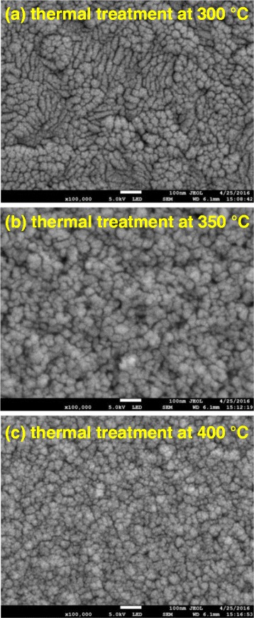
FESEM images of CuO-Cu2O complex thin films fabricated using thermal oxidation at various temperatures. a Thermal treatment at 300 °C. b Thermal treatment at 350 °C. c Thermal treatment at 400 °C
Fig. 5.
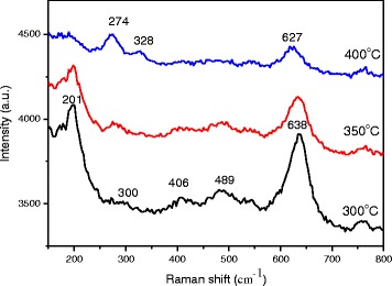
Raman scattering spectra of CuO-Cu2O complex thin films under 473-nm excitation
Fig. 6.
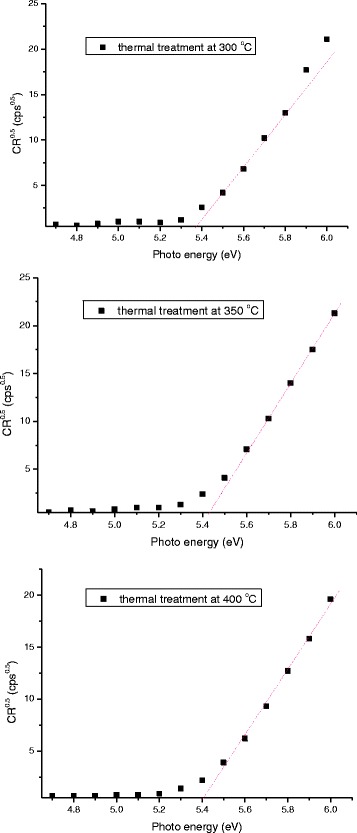
Photoelectron emission spectra of CuO-Cu2O complex thin films
Conclusions
This study examined the characteristics of a nano-structured CuO-Cu2O complex thin-film for use in perovskite solar cells. A CH3NH3PbI3 perovskite absorber was fabricated on top of a CuO-Cu2O complex thin film in a one-step spin-coating process, which was followed by toluene washing treatment. The work function of the Cu-Cu2O complex thin film varied with the annealing temperature. The work function of a CuO-Cu2O complex thin film is proportional to the Voc of the perovskite solar cell in which it is used. Following optimization, the maximum power conversion efficiency (PCE) exceeded 8.1 %. Therefore, the low-cost, solution-processed, stable nano-structured CuO-Cu2O complex thin film can be used in alternative hole transport layers (HTLs) in industrially produced perovskite solar cells.
Acknowledgements
The authors gratefully acknowledge the financial support from the Ministry of Science and Technology of the Republic of China under Contract No. NSC 105-2221-E-027-055.
Funding
This work was supported by the financial plan of the Ministry of Science and Technology of the Republic of China.
Authors’ Contributions
LCC wrote the paper, designed the experiments, and analyzed the data. CCC, KCL, SHC, ZLT, and WTW prepared the samples and did all the measurements. SCY, CTC, and CGW made the discussion and suggested the parameter. All authors read and approved the final manuscript.
Competing Interests
The authors declare that they have no competing interests.
Ethics Approval
Not applicable.
Abbreviations
- Cu2O
cuprous oxide
- CuO
copper oxide
- ETL
electron-transporting layer
- FESEM
field-emission scanning electron microscope
- HTL
hole transport layer
- ITO
indium tin oxide
- J-V
current density–voltage
- PCE
power conversion efficiency
- XRD
X-ray diffractometer
Contributor Information
Lung-Chieh Chen, Phone: +886-227-712-171, Email: ocean@ntut.edu.tw.
Cheng-Chiang Chen, Email: chiang0414@ncu.edu.tw.
Kai-Chieh Liang, Email: t103658001@ntut.edu.tw.
Sheng Hsiung Chang, Email: shchang@ncu.edu.tw, Email: shchang@ncu.edu.tw.
Zhong-Liang Tseng, Email: tw78787788@yahoo.com.tw.
Shih-Chieh Yeh, Email: imidjay@gate.sinica.edu.tw.
Chin-Ti Chen, Email: chintchen@gate.sinica.edu.tw.
Wen-Ti Wu, Email: wenti.wu@gmail.com.
Chun-Guey Wu, Email: t610002@cc.ncu.edu.tw.
References
- 1.Kojima A, Teshima K, Shirai Y, Miyasaka T. Organometal halide perovskites as visible-light sensitizers for photovoltaic cells. J Am Chem Soc. 2009;131:6050–6051. doi: 10.1021/ja809598r. [DOI] [PubMed] [Google Scholar]
- 2.Etgar L, Gao P, Xue Z, Peng Q, Chandiran AK, Liu B, Nazeeruddin MK, Gratzel M. Mesoscopic CH3NH3PbI3/TiO2 heterojunction solar cells. J Am Chem Soc. 2012;134:17396–17399. doi: 10.1021/ja307789s. [DOI] [PubMed] [Google Scholar]
- 3.Im JH, Lee CR, Lee JW, Park SW, Park NG. 6.5% efficient perovskite quantum-dot-sensitized solar cell. Nanoscale. 2011;3:4088–4093. doi: 10.1039/c1nr10867k. [DOI] [PubMed] [Google Scholar]
- 4.Lee MM, Teuscher J, Miyasaka T, Murakami TN, Snaith HJ. Efficient hybrid solar cells based on meso-superstructured organometal halide perovskites. Science. 2012;338:643–647. doi: 10.1126/science.1228604. [DOI] [PubMed] [Google Scholar]
- 5.Kim HS, Lee CR, Im JH, Lee KB, Moehl T, Marchioro A, Moon SJ, Humphry-Baker R, Yum JH, Moser JE, Gratzel M, Park NG. Lead iodide perovskite sensitized all- solid-state submicron thin film mesoscopic solar cell with efficiency exceeding 9 % Sci Rep. 2012;2:591. doi: 10.1038/srep00591. [DOI] [PMC free article] [PubMed] [Google Scholar]
- 6.Jeng JY, Chiang YF, Lee MH, Peng SR, Guo TF, Chen P, Wen TC. CH3NH3PbI3 perovskite/fullerene planar-heterojunction hybrid solar cells. Adv Mater. 2013;25:3727–3732. doi: 10.1002/adma.201301327. [DOI] [PubMed] [Google Scholar]
- 7.Zhou H, Chen Q, Li G, Luo S, Song T-B, Duan H-S, Hong Z, You J, Liu Y, Yang Y. Interface engineering of highly efficient perovskite solar cells. Science. 2014;345:542–546. doi: 10.1126/science.1254050. [DOI] [PubMed] [Google Scholar]
- 8.Liu D, Kelly TL. Perovskite solar cells with a planar heterojunction structure prepared using room-temperature solution processing techniques. Nat Pho- tonics. 2014;8:133–138. doi: 10.1038/nphoton.2013.342. [DOI] [Google Scholar]
- 9.Burschka J, Pellet N, Moon S-J, Humphry-Baker R, Gao P, Nazeeruddin MK, Gratzel M. Sequential deposition as a route to high-performance perovskite-sensitized solar cells. Nature. 2013;499:316–319. doi: 10.1038/nature12340. [DOI] [PubMed] [Google Scholar]
- 10.Chavhan S, Miguel O, Grande HJ, Gonzalez-Pedro V, Sánchez RS, Barea EM, Mora-Seró I, Tena-Zaera R. Organo-metal halide perovskite-based solar cells with CuSCN as the inorganic hole selective contact. J Mater Chem A. 2014;2:12754–12760. doi: 10.1039/C4TA01310G. [DOI] [Google Scholar]
- 11.Ito S, Tanaka S, Manabe K, Nishino H. Effects of surface blocking layer of Sb2S3 on nanocrystalline TiO2 for CH3NH3PbI3 perovskite solar cells. J Phys Chem C. 2014;118:16995–17000. doi: 10.1021/jp500449z. [DOI] [Google Scholar]
- 12.Docampo P, Ball JM, Darwich M, Eperon GE, Snaith HJ (2013) Efficient organometal trihalide perovskite planar-heterojunction solar cells on flexible polymer substrates. Nat Commun 4:2761 [DOI] [PubMed]
- 13.Christians JA, Fung RCM, Kamat PV. An inorganic hole conductor for organo-lead halide perovskite solar cells. Improved hole conductivity with copper iodide. J Am Chem Soc. 2014;136:758–764. doi: 10.1021/ja411014k. [DOI] [PubMed] [Google Scholar]
- 14.Qin P, Tanaka S, Ito S, Tetreault N, Manabe K, Nishino H, Nazeeruddin MK, Gratzel M. Inorganic hole conductor-based lead halide perovskite solar cells with 12.4% conversion efficiency. Nat Commun. 2014;5:3834. doi: 10.1038/ncomms4834. [DOI] [PubMed] [Google Scholar]
- 15.Subbiah AS, Halder A, Ghosh S, Mahuli N, Hodes G, Sarkar SK. Inorganic hole conducting layers for perovskite-based solar cells. J Phys Chem Lett. 2014;5:1748–1753. doi: 10.1021/jz500645n. [DOI] [PubMed] [Google Scholar]
- 16.Ye SY, Sun WH, Li YL, Yan WB, Peng HT, Bian ZQ, Liu ZW, Huang CH. CuSCN-based inverted planar perovskite solar cell with an average PCE of 15.6% Nano Lett. 2015;15:3723–3728. doi: 10.1021/acs.nanolett.5b00116. [DOI] [PubMed] [Google Scholar]
- 17.Wu Z, Bai S, Xiang J, Yuan Z, Yang Y, Cui W, Gao X, Liu Z, Jin Y, Sun B. Efficient planar heterojunction perovskite solar cells employing graphene oxide as hole conductor. Nanoscale. 2014;6:10505–10510. doi: 10.1039/C4NR03181D. [DOI] [PubMed] [Google Scholar]
- 18.Wang KC, Jeng JY, Shen PS, Chang YC, Diau EWG, Tsai CH, Chao TY, Hsu HC, Lin PY, Chen P, Guo TF, Wen TC. P-type mesoscopic nickel oxide/organometallic perovskite heterojunction solar cells. Sci Rep. 2014;4:4756. doi: 10.1038/srep04756. [DOI] [PMC free article] [PubMed] [Google Scholar]
- 19.Zuo C, Ding L. Solution-processed Cu2O and CuO as hole transport materials for efficient perovskite solar cells. Small. 2015;11:5528–5532. doi: 10.1002/smll.201501330. [DOI] [PubMed] [Google Scholar]
- 20.P. E. de Jongh, D. Vanmaekelbergh and J. J. Kelly, (1999) Cu2O: a catalyst for the photochemical decomposition of water?, Chem Commun 1069–1070.
- 21.Akimoto K, Ishizuka S, Yanagita M, Nawa Y, Paul GK, Sakurai T. Thin film deposition of Cu2O and application for solar cells. Sol Energy. 2006;80:715–722. doi: 10.1016/j.solener.2005.10.012. [DOI] [Google Scholar]
- 22.Jiang T, Xie T, Zhang Y, Chen L, Peng L, Li H, Wang D. Photoinduced charge transfer in ZnO/Cu2O heterostructure films studied by surface photovoltage technique. Phys Chem Chem Phys. 2010;12:15476–15481. doi: 10.1039/c0cp01228a. [DOI] [PubMed] [Google Scholar]
- 23.Ishizuka S, Kato S, Maruyama T, Akimoto K. Nitrogen doping into Cu2O thin films deposited by reactive radio-frequency magnetron sputtering. Jpn J Appl Phys. 2001;40:2765–2768. doi: 10.1143/JJAP.40.2765. [DOI] [Google Scholar]
- 24.Nakaoka K, Ogura K. Electrochemical preparation of p- type cupric and cuprous oxides on platinum and gold substrates from copper(II) solutions with various amino acids. J Electrochem Soc. 2002;149:C579–C585. doi: 10.1149/1.1512670. [DOI] [Google Scholar]
- 25.Mukhopadhyay AK, Chakraborty AK, Chatterjee AP, Lahiri SK. Galvanostatic deposition and electrical characterization of cuprous oxide thin films. Thin Solid Films. 1992;209:92–96. doi: 10.1016/0040-6090(92)90015-4. [DOI] [Google Scholar]
- 26.Joseph S, Kamath PV. Electrochemical deposition of Cu2O on stainless steel substrates: promotion and suppression of oriented crystallization. Solid State Sci. 2008;9:1215–1221. doi: 10.1016/j.solidstatesciences.2007.11.007. [DOI] [Google Scholar]
- 27.Fujiwara T, Nakaue T, Yoshimura M. Direct fabrication and patterning of Cu2O film by local electrodeposition method. Solid State Ionics. 2004;175:541–544. doi: 10.1016/j.ssi.2004.01.081. [DOI] [Google Scholar]
- 28.Zhang L, Li H, Ni Y, Li J, Liao K, Zhao G. Porous cuprous oxide microcubes for non-enzymatic amperometric hydrogen peroxide and glucose sensing. Electrochemistry Com- munications. 2009;11:812–815. doi: 10.1016/j.elecom.2009.01.041. [DOI] [Google Scholar]
- 29.Kuo CH, Huang MH. Fabrication of truncated rhombic dodecahedral Cu2O nanocages and nanoframes by particle aggregation and acidic etching. J Am Chem Soc. 2008;130:12815–12820. doi: 10.1021/ja804625s. [DOI] [PubMed] [Google Scholar]
- 30.Jimenez-Cadena G, Comini E, Ferroni M, Sberveglieri G. Synthesis of Cu2O bi-pyramids by reduction of Cu(OH)2 in solution. Mater Lett. 2010;64:469–471. doi: 10.1016/j.matlet.2009.11.051. [DOI] [Google Scholar]
- 31.Chen CC, Chen LC, Lee YH. Annealing effects of sputtered Cu2O nanocolumns on ZnO-coated glass substrate for solar cell applications. Adv Condense Matter Phys. 2012;2012:129139. doi: 10.1155/2012/129139. [DOI] [Google Scholar]
- 32.Chatterjee S, Pal AJ. Introducing Cu2O thin films as a hole-transport layer in efficient planar perovskite solar cell structures. J Phys Chem C. 2016;120:1428–1437. doi: 10.1021/acs.jpcc.5b11540. [DOI] [Google Scholar]
- 33.Singh F, Kulriya PK, Pivin JC. Origin of swift heavy ion induced stress in textured ZnO thin films: an in situ X-ray diffraction study. Solid State Commun. 2010;150:1751–1754. doi: 10.1016/j.ssc.2010.07.026. [DOI] [Google Scholar]
- 34.Xu JF, Ji W, Shen ZX, Li WS, Tang SH, Ye XR, Jia DZ, Xin XQ. Raman spectra of CuO nanocrytals. J Raman Spectrosc. 1999;30:413–415. doi: 10.1002/(SICI)1097-4555(199905)30:5<413::AID-JRS387>3.0.CO;2-N. [DOI] [Google Scholar]
- 35.Mao J, He J, Sun X, Li W, Lu X, Gan J, Liu Z, Gong L, Chen J, Liu P, Tong Y. Electrochemical synthesis of hierarchical Cu2O stars with enhanced photoelectrochemical properties. Electrochim Acta. 2012;62:1–7. doi: 10.1016/j.electacta.2011.10.106. [DOI] [Google Scholar]


