Abstract
Organic-inorganic hybrid perovskites have the potential to be used as a new class of emitters with tunable emission, high color purity and good ease of fabrication. Recent studies have so far been focused on three-dimensional (3D) perovskites, such as CH3NH3PbBr3 and CH3NH3PbI3 for green and infrared emission. Here, we explore a new series of hybrid perovskite emitters with a general formula of (C4H9NH3)2(CH3NH3)n−1PbnI3n+1 (where n = 1, 2, 3), which possesses a multiple quantum well structure. The quantum well thickness of these materials is adjustable through simple molecular engineering which results in a continuously tunable bandgap and emission spectra. Deep saturated red emission was obtained with a peak external quantum efficiency of 2.29% and a maximum luminance of 214 cd/m2. Green and blue LEDs were also demonstrated through halogen substitutions in these hybrid perovskites. We expect these results to open up the way towards high performance perovskite LEDs through molecular-structure engineering of these perovskite emitters.
Organic-inorganic hybrid perovskite is an interesting class of materials because of their unique molecular structure whereby organic molecules are incorporated into inorganic crystals. In recent years, numerous studies have shown the viability of this material system in functional devices due to their exceptional optical and electrical properties, including high charge mobility, tunable band structure and high luminance efficiency1,2,3,4,5,6,7. On top of these functional properties, the solution processability of these hybrid perovskites also enables them to be promising candidates for the next-generation low-cost optoelectronic devices suitable for large-scale production. Since the first introduction of three-dimensional (3D) hybrid perovskites (CH3NH3PbI3 and CH3NH3PbBr3) for photovoltaic applications in 2009, this material system has been seen as a wonder material in the field with a high power conversion efficiency of up to 20% and this is achieved in just a few years8,9,10,11,12,13. This success has also triggered researchers to further explore the application of hybrid perovskites in other areas including light-emitting diode (LED) and laser14,15,16. Recently, room-temperature infrared and green electroluminescence from the 3D hybrid perovskites have been reported confirming their potential for highly efficient, low-cost LED devices14. The performance of 3D perovskite LEDs has been dramatically improved through controlled film formation and employing nano-sized crystals to confine the exciton diffusion length17,18. Perovskite LEDs with a high current efficiency (CE) of 42.9 cd/A were demonstrated very recently, and this once again reinforces the belief that they have strong potential to compete as a new material in light-emission devices19.
Despite recent rigorous explorations of 3D perovskites, the first perovskite-based LED demonstrated in 1994 was in fact based on layered hybrid perovskite ((C6H5C2H4NH3)2PbI4), which inherently possessed a two-dimensional (2D) quantum well structure20. Within those quantum wells, electrons and holes are strongly confined in two dimensions rendering a large exciton binding energy and hence high luminescence yield. Furthermore, multiple quantum well structure, as in the case of conventional inorganic LEDs, has also demonstrated other advantages such as suppression of charge flow and improvement of radiative recombination21. However at that time, the efficient electroluminescence from those 2D perovskite LEDs could only be preserved at cryogenic temperature possibly due to exciton quenching at room temperature20. Therefore, this poses a huge challenge for practical applications of these materials as light emitting devices.
Extending the pioneering work on both 3D and 2D perovskites, herein we report the first demonstration of room-temperature light-emitting devices based on layered perovskites possessing multiple quantum well (MQW) structure. The quantum well thickness was adjusted by combining the 3D and 2D perovskites at molecular level, resulting in tunable light emission due to the quantum confinement effect. Red perovskite LED with high color purity was obtained with a maximum external quantum efficiency of 2.29% and a maximum luminance of 214 cd/m2. Green and blue LEDs based on MQW perovskite were also demonstrated for a solution-processed full-color perovskite display.
Results
Perovskite structures and optical properties
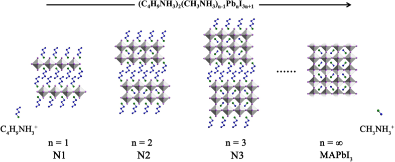
Hybrid perovskites are typically crystallized from the reaction between metal halide and organic halide molecules and subsequently self-organized into 0D, 1D, 2D or 3D structure depending on the connection of metal halide octahedra. For example, the reaction between a small organic molecule such as methylammonium iodide (CH3NH3I, MAI) and PbI2 will result in 3D methylammonium lead iodide (MAPbI3) perovskite where the PbI6 octahedron connects three-dimensionally with each other by corner-sharing (MAPbI3 in Fig. 1). Replacing MAI with larger organic molecules, such as butylammonium iodide (C4H9NH3I, BAI), interrupts the connection in one direction forming a layered structure with inorganic and organic components stacking alternately hence reducing the structural dimensionality (N1 in Fig. 1). In this case, each inorganic octahedra layer is separated by two layers of organic moiety; their interlayer interaction becomes weaker than in the 3D form22,23,24. Therefore, they can be regarded as “bulk 2D” materials comprising of sheet-like inorganic blocks with 2D characteristics. Due to the smaller band gap (Eg) of the inorganic layers compared to that of the organic layers, quantum wells are formed in these layered perovskites with organic layers acting as barriers confining the inorganic wells25. The combination of organic moieties with different sizes (e.g., MA+ and BA+) allows further fine-tuning of the structure as well as the thickness of the quantum well resulting in double octahedra stacking (N2), triple octahedra stacking (N3), and so on26,27. The generic chemical formula for these layered hybrid perovskites is (C4H9NH3)2(CH3NH3)n−1PbnI3n+1, where n represents the number of octahedra layers within each quantum well.
Figure 1. Crystal structures of 2D and 3D perovskites viewed from the side.
(C4H9NH3)2(CH3NH3)n−1PbnI3n+1, where n = 1 for N1, n = 2 for N2, n = 3 for N3 and n = ∞ for MAPbI3. The molecular structures of C4H9NH3+ and CH3NH3+ are presented with carbon and nitrogen atoms represented by blue and green balls, respectively, while hydrogen atoms are omitted for clarity.
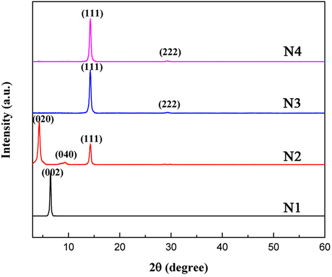
All the layered perovskite films were spin-coated from solutions containing PbI2 and organic halides (BAI for N1, BAI and MAI in respective ratios for N2, N3 and N4). From the change in color of the film, it can be deduced that the film crystallized almost instantaneously - within several seconds after the start of spin coating. The fast crystallization was induced by the self-assembly of both organic molecules and inorganic octahedra which could be advantageous for the proposed quantum well (QW) structure. Essentially, the van der Waals forces between long-chain organic molecules help to drive the organization in these perovskites. The perovskite structure is confirmed by X-ray diffraction (XRD) spectra as shown in Fig. 2. In general, all the layered perovskites showed a tendency to form highly oriented film with crystalline phases comprised of alternate layers of inorganic and organic moieties. For N1, only (002) peak corresponding to the stacking layers, is observed, which indicates high crystallinity and regular layer stacking. The corresponding peak for N2 (020) shifts to a smaller 2θ indicating an enlarged quantum well thickness with wider interplanar spacing. The additional peaks, such as (111) and (222), are due to the inorganic stacking layers and these diffraction peaks become stronger for N3 and N4. It also reveals that growth orientation gradually shifts from (001) to (111) plane with increasing number of octahedra layers (i.e., higher N), as confirmed by previous study27. It is worth noting that there is no observable mixed phase between these layered perovskites as confirmed from the high purity of each corresponding XRD pattern. The quantum well and barrier thicknesses can be derived from the XRD patterns as they correspond to the inorganic and organic layer thicknesses respectively. As expected, the QW thickness gradually increases from 0.62 nm for N1 to 2.49 nm for N4 with barrier thickness of around 0.7–0.8 nm. The quantum well and barrier thickness were calculated for the quantum well perovskites and included in the Supplementary Table S1.
Figure 2. XRD patterns of QW perovskites from N1 to N4.
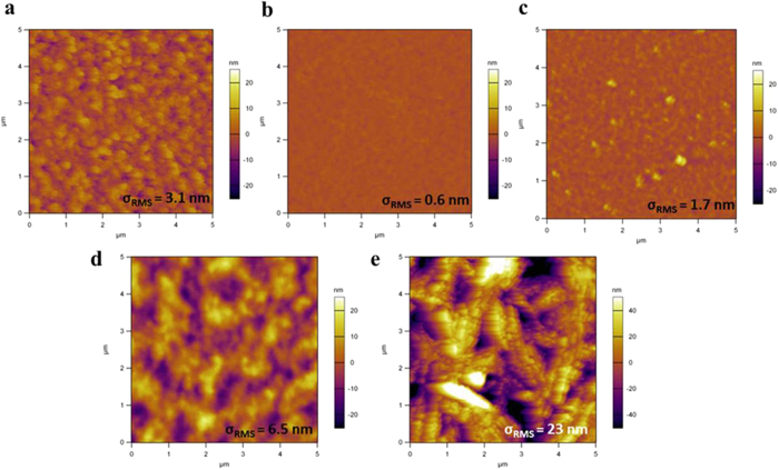
The self-assembly of these hybrid perovskites has a strong influence on the morphology. The N1 perovskite shows large microplates merging into a compact film with a root-mean-square roughness (σRMS) of 3.1 nm (Fig. 3a, Supplementary Fig. S2a). This unique feature derives from the highly ordered stacking layers. Interestingly, for N2 the combination of BAI and MAI results in a smoother film with a σRMS of 0.6 nm (Fig. 3b, Supplementary Fig. S2b,c). The small roughness of N2 comparable to its single layer thickness suggests a high film uniformity over a large area. The film surface roughness slightly increases for N3 and N4 with σRMS of 1.7 nm and 6.5 nm, respectively. By contrast, the MAPbI3 film is discontinuous and shows a much higher roughness with coverage of about 70% (Fig. 3e, corresponding electron micrograph is shown in Supplementary Fig. S2f). It is clear that the presence of two different organic molecules in the perovskite synthesis has dramatically influenced the film morphology. We believe this is because of the different roles assumed by BAI and MAI during the crystal growth that induce the PbI6 octahedra building block to assemble along the plane and c-axis simultaneously. The different sizes of the organic molecules also prevent the mixing of both the organic and inorganic layers resulting in almost perfect assembly of alternating hybrid organic and inorganic layers as confirmed from the distinct XRD peaks.
Figure 3. AFM images different perovskite thin films.
(a) N1, (b) N2, (c) N3, (d) N4 and (e) MAPbI3 with respective σRMS.
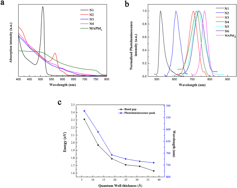
The optical properties of the layered perovskite films were examined and the absorption and luminescence data are shown in Fig. 4. Due to quantum confinement effect, the absorption onset of layered perovskites blue-shifted compared to that of MAPbI3. N1 perovskite shows an unusual absorption peak at 511 nm because of the strong photon-exciton interaction confined within the 2D quantum wells. This attributes to the long lifetime and large binding energy (~300 meV) of the excitons23. With the increase in the thickness of the quantum wells, this peak becomes weaker and eventually subsides for N3 and N4. The large binding energy is beneficial to promote radiative recombination, as evidenced by the photoluminescence (PL) of the QW perovskites at room temperature. The position of the PL peak (λmax) corresponds well to the optical absorption, while the full width at half maximum (FWHM) of the corresponding peak increases from 28 nm for N1 to 74 nm for N6. The correlation between the optical band gap (Eg), λmax and the quantum well thickness is summarized in Fig. 4c. The optical band gap of QW perovskites gradually decreases from 2.3 eV to 1.6 eV approaching the band gap of 3D MAPbI3 (~1.55 eV) because of the weaker quantum confinement in the perovskites with thicker quantum wells28. The same thickness-dependent trend is also observed for λmax of the PL spectra suggesting that a simple adjustment of the quantum well thickness is able to yield a well-defined emission of the QW perovskites.
Figure 4. Optical properties of perovskite thin films.
(a) Optical absorption and (b) photoluminescence spectra of different perovskites thin films. (c) Optical band gap, photoluminescence peak position and their relationships with the quantum well thickness.
Device performance of quantum well perovskite LEDs
To demonstrate their application in light emitting devices, we fabricated QW perovskite LEDs with a multi-layered structure of ITO/poly(ethylenedioxythiophene):polystyrene sulfonate (PEDOT:PSS, 40 nm)/poly(N,N′-bis(4-butylphenyl)-N,N′-bis(phenyl)-benzidine) (poly-TPD, 30 nm)/QW-perovskite (100 nm)/1,3,5-tris(1-phenyl-1H-benzimidazol-2-yl)benzene (TPBi, 40 nm)/LiF (1 nm)/Al (100 nm), as shown in Fig. 5a,b. Figure 5c shows a schematic of the energy level diagram of all the layers and for the purpose of the diagram, the energy level for QW-perovskite layer is represented by that of N3 obtained from literature27. PEDOT:PSS and poly-TPD are solution processed sequentially and they act effectively as the hole-injection layer (HIL) and hole-transport layer (HTL) respectively. Due to its high work function and low electron affinity, the poly-TPD layer reduces the hole-injection barrier from the anode and blocks electrons from the perovskite emitter. A thin layer of TPBi is evaporated on top of perovskite layer to serve as the electron-transporting layer (ETL).
Figure 5. QW perovskite LED structure.
(a) Schematic of device structure and (b) their cross-section scanning electron image, scale bar: 100 nm. (c) Energy levels of corresponding layers in QW perovskite LEDs.
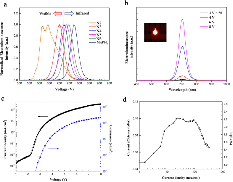
No electroluminescence (EL) was observed from N1 based device which is consistent with previous report20. However, the remaining layered perovskites in our study (N2–N6) all showed red luminescence and their corresponding EL spectra are shown in Fig. 6a. The N2 perovskite demonstrates an unusual double peak with a broad coverage from 550 nm to 800 nm. The inconsistency between the λmax of EL and PL suggests that the presence of electric field has influenced the electronic structures of N2, which could also explain the absence of EL in N1 device29−32. The quantum well thickness of N1 and N2 perovskites is only 6.2 Å and 12.4 Å, respectively. Within the narrow quantum wells, the excitons are highly squeezed. The amount of electric field required to drive an LED is enough to cause a massive perturbation on these excitons. Thus the presence of electric field changes their emission characteristics or field-ionizes those excitons, which has been confirmed in the conventional inorganic quantum wells33. Further study of the effect of electrical field on the excitons in hybrid multiple quantum well structure is currently being pursued.
Figure 6. QW perovskite LED characteristics.
(a) Electroluminescence spectra of QW perovskites and MAPbI3. (b) Electroluminescence intensity of N3 LED under different voltages; inset shows a N3 LED operated at 6 V. (c) J-V-L characteristics of N3 perovskite LED. (d) Current efficiency and EQE of N3 LED.
For layered perovskites with thicker quantum wells (N3 to N6), their EL spectra correspond well with their respective PL spectra with a narrow peak of FWHM around 50 nm. The dash line in Fig. 6a at 720 nm represents the limit of human visual sensitivity to visible light. Almost the whole emission spectrum of MAPbI3 falls into infrared wavelength thus limiting its application in visible displays. By employing quantum well structure, the emission could be gradually shifted into visible wavelength with peaks at 746 nm, 735 nm, 723 nm and 700 nm for N6, N5, N4 and N3, respectively. In particular, the N3 perovskite LED emits deep, saturated red color and 77% of the emitted photons are in the visible spectrum (620 nm to 720 nm). Different operating voltages (3–8V) did not induce any noticeable peak shift in the N3 perovskite LED, as shown in Fig. 6b. The inset shows a small N3 perovskite LED operated at 6 V. It is worth noting that this is the first successful demonstration of a stable pure red emission from perovskite LEDs. Previous study has shown that the red LED fabricated with mixed Br/I perovskite was not stable due to the large discrepancy in the size of both halogens resulting in the film undergoing phase separation under light soaking34. Previous approach towards red perovskite LEDs based on Br/I mixed system also resulted in a broad emission spectrum with mixed colors or intermediate orange color14,17. In our layered perovskite LEDs, pure iodide perovskite was used while the fine tuning of the emission into deep red wavelength region was achieved by adjusting the QW thickness. These devices also yielded highly pure emission with narrow FWHM of 50 nm, which indicates strong quantum confinement effect as well as extremely low amount of impurities in our layered perovskite materials.
The current density-voltage-luminance (J-V-L) characteristics of our best LED device based on N3 perovskite are presented in Fig. 6c. The device shows a turn-on voltage (Von) of 2.7 V in agreement with the onset of current, suggesting a balanced injection of electrons and holes. The luminance increases steeply after Von and reaches 214 cd/m2 at 8 V. The current efficiency (CE) and external quantum efficiency (EQE) increases with current density and yields a maximum CE of 0.1 cd/A and EQE of 2.29% at 21.7 mA/cm2 (Fig. 6d). The highest current efficiency could be well maintained (>80%) from 10 mA/cm2 to 100 mA/cm2, corresponding to a wide range of brightness from 7 cd/m2 to 150 cd/m2. However, the device shows a dramatic efficiency roll-off at high current density above 100 mA/cm2. We speculate that the root cause for this is the increased imbalance between the injection of electrons and holes at higher operating voltage which leads to more non-radiative recombination at the interface. We believe a deeper understanding of device working mechanism as well as the photo-physics of layered perovskite could be beneficial in preventing the efficiency roll-off thus improving its performance.
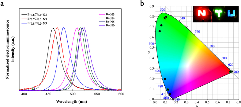
For full-color display application, we extend the quantum well structure from iodide-based perovskite to Br and Br/Cl-mixed perovskites to obtain green and blue emission. The same device structure was adopted, i.e., layered perovskite sandwiched between poly-TPD and TPBi. All the layered perovskites exhibit smooth and compact thin films, a strong contrast to the isolated perovskite islands observed in 3D MAPbBr3 with a poor coverage of less than 50% (Figure S4). The blue and green EL spectra are shown in Fig. 7a. In the case of bromide-based QW perovskites, similar trend to that of iodide-based perovskites was observed. No emission was detected from Br-N1 and double peak was observed from Br-N2 (see Supplementary Fig. S5). The EL spectra peak (λmax) monotonically shifts from 508 nm to 525 nm in the green region for Br-N3 to Br-N6, with a narrow FWHM of ~20 nm. To further drive the emission into the blue region, we mixed a small amount of Cl in Br-N3 and obtained blue emission at 460 nm, 469 nm and 480 nm from Br0.6Cl0.4-N3, Br0.7Cl0.3-N3 and Br0.8Cl0.2-N3, respectively. The device characteristics of our best green and blue LEDs together with the red LEDs are summarized in Table 1. The green LED shows a peak EQE of 1.01%, corresponding to a peak current efficiency of 3.48 cd/A, with a maximum luminance of 2246 cd/m2. However, the blue LED has a much lower EQE (0.01%), probably due to the increase in charge injection barrier at both sides which leads to a higher Von of 5.2 V and more quenching of the excitons. We believe the operating voltage as well as the EQE could be improved by replacing the charge injection layers that possess better band alignment with those blue emitting perovskites. As our layered perovskites tend to form uniform films over large area, we fabricated large-area LEDs on 2.5 × 2.5 cm2 substrates with patterned electrodes as shown in Fig. 7b. The luminescent logo was constructed with red, green and blue LEDs prepared from I-N3, Br-N5 and Br0.7Cl0.3-N3 perovskites, respectively. Their high color purity is indicated on the Commission Internationale de l’Eclairage (CIE) diagram by stars while the black circles represent the series of layered perovskites. This demonstrates the promising application for large-area full-color display based solely on hybrid perovskites. The long-term operational stability is a critical concern for hybrid perovskite based photovoltaics and LEDs. Although our layered perovskites show a steady photoluminescence as contrast to the quickly decaying emission for 3D perovskite of MAPb(I0.5Br0.5)3, the device luminescence dropped to ~20% of its initial value after 3 min (see Supplementary Fig. S6). Compared with previous reports where the stability of perovskite LED were only tested under pulsed voltage, our device already showed an improvement mainly due to the smooth, full-coverage perovskite film14. Further study to optimize the devices for balanced charge injection and reduced excess current is expected to improve their stability.
Figure 7. Green and blue LEDs based on QW perovskites.
(a) Electroluminescence spectra of Br perovskites and BrxCl1−x perovskites. (b) CIE coordinates of red, green and blue LEDs based on QW series perovskites; inset shows the photograph of QW perovskite LEDs with Nanyang Technological University (NTU) logo.
Table 1. Characteristics of red, green and blue perovskite LEDs: emitting perovskite compositions, peak EL wavelength (λmax) and FWHM, turn-on voltage (Von), peak EQE, peak CE and maximum luminance (L).
| Color of Perovskite LEDs | Emitting Perovskite Composition | EL λmax (FWHM) | Von | Peak EQE | Peak CE | Max. L |
|---|---|---|---|---|---|---|
| Red | (BA)2(MA)2Pb3I10 | 700 nm (52 nm) | 2.7 V | 2.29% | 0.1 cd/A | 214 cd/m2 |
| Green | (BA)2(MA)4Pb5Br16 | 523 nm (24 nm) | 3.3 V | 1.01% | 3.48 cd/A | 2246 cd/m2 |
| Blue | (BA)2(MA)2Pb3Br7Cl3 | 468 nm (28 nm) | 5.2 V | 0.01% | 0.006 cd/A | 21 cd/m2 |
Conclusion
In summary, we fabricated red, green and blue LEDs with hybrid perovskites possessing multiple quantum well (MQW) structure for the first time. These layered perovskites are beneficial in terms of the flexibility in fine-tuning their light emission properties. Furthermore, it also enables the preparation of uniform and smooth film over large area thus making it suitable for scalable manufacturing. We believe that the unique multiple quantum well structure of hybrid perovskite is the way to high-performance light emitting devices. Furthermore, the present study has also opened up a favorable outlook on charge-injection perovskite laser diodes in which multiple quantum wells could be used as optical cavities to amplify light output.
Methods
Materials and synthesis
PEDOT:PSS (Clevios PVP Al 4083) was purchased from Heraeus Holding GmbH and used as received. Poly-TPD and TPBi were purchased from American Dye Source and Lumtec, respectively. Other chemicals were purchased from Sigma-Aldrich and used as received. CH3NH3I (MAI) and C4H9NH3I (BAI) were synthesized from the reaction of methylamine and n-butylamine, respectively, with excess hydriodic acid (HI) (47wt% in water) at 0 °C with (molar ratio of amine to HI = 1:1.2). CH3NH3Br (MABr) and C4H9NH3Br (BABr) were synthesized similarly with HBr (48wt% in water). The crude product was obtained by slowly evaporating the solvent under reduced pressure. Then the white precipitate was dissolved in ethanol and recrystallized by adding diethyl ether. The small crystals were further washed with diethyl ether several times before drying them in vacuum oven. After drying overnight, they were all sealed under nitrogen and transferred into an N2 glove box for further use. (BA)2(MA)n−1PbnI3n+1 precursor solution was prepared by dissolving BAI, MAI and PbI2 (99%) with respective stoichiometric ratio in DMF. (BA)2(MA)n−1PbnBr3n+1 precursor solution was prepared similarly using MABr, BABr and PbBr2 (99.999%). Mixed Br/Cl perovskite precursor solution was prepared similarly except for the mixing of PbCl2 (99.999%) and PbBr2 in the solution in a specific ratio. All perovskite precursor solutions were heated at 70 °C before use.
Device fabrication
To prepare the LED devices, PEDOT:PSS solution was first spin coated onto patterned ITO substrates at 4000 rpm for 60 s, followed by baking at 150 °C for 10 min. After cooling to room temperature, the PEDOT:PSS-coated substrates were transferred into N2 filled glove box. Poly-TPD solution (7 mg/ml in chlorobenzene) was spin coated on top of the substrate at 5000 rpm followed by annealing at 110 °C for 30 min. Prior to the perovskite coating, the poly-TPD surface was treated in UV-ozone cleaner for 10 s. The perovskite solution was deposited on the treated substrate at 8000 rpm for 60 s. The perovskite film thickness was controlled by varying the solution concentration. Typically 0.3 M (for Pb2+) of N3 perovskite solution results in a film of 100 nm, as examined from scanning electron microscope (SEM) cross section. To obtain comparable thickness, the solution concentrations of N2 and N1 have to be reduced to 0.25 M and 0.2 M, respectively. The LED devices were completed by evaporating TPBi (40 nm), LiF (1 nm) and Al (100 nm) sequentially under high vacuum (1 × 10⁻⁶ mbar). The active area was 7 mm2 as defined by the overlapping between back electrode and ITO.
Characterization and device measurement
XRD patterns of the as-deposited perovskite films were collected on Shimadzu XRD-6000 with an incident angle of 1° at 2θ mode. The scan speed was set to 2°/min. SEM and atomic force microscopy (AFM) images were taken on JEOL 7600F and Asylum MFP-3D, respectively. Absorption and photoluminescence spectra were obtained by using Agilent Cary 5000 UV-Vis-NIR and Cary Eclipse Fluorescence Spectrometer. The EL spectra of the LED devices were recorded with Ocean Optics Maya 2000 Pro Spectrometer under working voltages applied by a Keithley 2400 sourcemeter. The current density-voltage-luminance characteristics were collected using a Keithley 2400 sourcemeter, an integrating sphere connected with Maya 2000 Pro Spectrometer through an optical fibre. The corresponding luminance was calibrated with a standard vis-NIR light source (HL-3-INT-CAL, Ocean Optics).
Additional Information
How to cite this article: Hu, H. et al. Molecularly Engineered Organic-Inorganic Hybrid Perovskite with Multiple Quantum Well Structure for Multicolored Light-Emitting Diodes. Sci. Rep. 6, 33546; doi: 10.1038/srep33546 (2016).
Supplementary Material
Acknowledgments
Y.M.L. acknowledges financial support from a MOE AcRF Tier 1 grant (RG99/14).
Footnotes
Author Contributions H.H. and Y.M.L. conceived the idea; H.H. performed the experiments; all authors contributed the analysis of results. H.H., T.S. and Y.M.L. prepared and commented the manuscript.
References
- Mitzi D. B. Synthesis, structure, and properties of organic-inorganic perovskites and related materials. Prog. Inorg. Chem 48, 1–121 (1999). [DOI] [PubMed] [Google Scholar]
- Xing G. C. et al. Long-Range Balanced Electron- and Hole-Transport Lengths in Organic-Inorganic CH3NH3PbI3. Science 342, 344–347 (2013). [DOI] [PubMed] [Google Scholar]
- Eperon G. E. et al. Formamidinium lead trihalide: a broadly tunable perovskite for efficient planar heterojunction solar cells. Energy Environ. Sci. 7, 982–988 (2014). [Google Scholar]
- Noh J. H., Im S. H., Heo J. H., Mandal T. N. & Seok S. I. Chemical management for colorful, efficient, and stable inorganic-organic hybrid nanostructured solar cells. Nano Lett. 13, 1764–1769 (2013). [DOI] [PubMed] [Google Scholar]
- Deschler F. et al. High Photoluminescence Efficiency and Optically Pumped Lasing in Solution-Processed Mixed Halide Perovskite Semiconductors. J. Phys. Chem. Lett. 5, 1421–1426 (2014). [DOI] [PubMed] [Google Scholar]
- Dou L. T. et al. Atomically thin two-dimensional organic-inorganic hybrid perovskites. Science 349, 1518–1521 (2015). [DOI] [PubMed] [Google Scholar]
- Li Y. et al. Direct Observation of Long Electron-Hole Diffusion Distance in CH3NH3PbI3 Perovskite Thin Film. Sci Rep. 5, 14485 (2015). [DOI] [PMC free article] [PubMed] [Google Scholar]
- Kojima A., Teshima K., Shirai Y. & Miyasaka T. Organometal Halide Perovskites as Visible-Light Sensitizers for Photovoltaic Cells. J. Am. Chem. Soc. 131, 6050–6051 (2009). [DOI] [PubMed] [Google Scholar]
- Sun S. Y. et al. The origin of high efficiency in low-temperature solution-processable bilayer organometal halide hybrid solar cells. Energy Environ. Sci. 7, 399–407 (2014). [Google Scholar]
- Zhou H. P. et al. Interface engineering of highly efficient perovskite solar cells. Science 345, 542–546 (2014). [DOI] [PubMed] [Google Scholar]
- Jeon N. J. et al. Compositional engineering of perovskite materials for high-performance solar cells. Nature 517, 476–480 (2015). [DOI] [PubMed] [Google Scholar]
- Kim H. S. et al. Lead iodide perovskite sensitized all-solid-state submicron thin film mesoscopic solar cell with efficiency exceeding 9%. Sci Rep. 2, 591 (2012). [DOI] [PMC free article] [PubMed] [Google Scholar]
- Ku Z., Rong Y., Xu M., Liu T. & Han H. Full printable processed mesoscopic CH3NH3PbI3/TiO2 heterojunction solar cells with carbon counter electrode. Sci Rep. 3, 3132 (2013). [DOI] [PMC free article] [PubMed] [Google Scholar]
- Tan Z. K. et al. Bright light-emitting diodes based on organometal halide perovskite. Nat. Nanotechnol 9, 687–692 (2014). [DOI] [PubMed] [Google Scholar]
- Wang J. P. et al. Interfacial Control Toward Efficient and Low-Voltage Perovskite Light-Emitting Diodes. Adv. Mater. 27, 2311–2316 (2015). [DOI] [PubMed] [Google Scholar]
- Xing G. C. et al. Low-temperature solution-processed wavelength-tunable perovskites for lasing. Nat. Mater. 13, 476–480 (2014). [DOI] [PubMed] [Google Scholar]
- Song J. et al. Quantum Dot Light-Emitting Diodes Based on Inorganic Perovskite Cesium Lead Halides (CsPbX ). Adv. Mater. 27, 7162–7167 (2015). [DOI] [PubMed] [Google Scholar]
- Li G. et al. Efficient light-emitting diodes based on nanocrystalline perovskite in a dielectric polymer matrix. Nano Lett. 15, 2640–2644 (2015). [DOI] [PubMed] [Google Scholar]
- Cho H. C. et al. Overcoming the electroluminescence efficiency limitations of perovskite light-emitting diodes. Science 350, 1222–1225 (2015). [DOI] [PubMed] [Google Scholar]
- Era M., Morimoto S., Tsutsui T. & Saito S. Organic-inorganic heterostructure electroluminescent device using a layered perovskite semiconductor (C6H5C2H4NH3)2PbI4. Appl. Phys. Lett. 65, 676–678 (1994). [Google Scholar]
- Han S. H. et al. Effect of electron blocking layer on efficiency droop in InGaN/GaN multiple quantum well light-emitting diodes. Appl. Phys. Lett. 94 (2009). [Google Scholar]
- Ishihara T. Optical-Properties of Pbi-Based Perovskite Structures. J. Lumin 60–1, 269–274 (1994). [Google Scholar]
- Wu X., Trinh M. T. & Zhu X. Y. Excitonic Many-Body Interactions in Two-Dimensional Lead Iodide Perovskite Quantum Wells. J. Phys. Chem. C 119, 14714–14721 (2015). [Google Scholar]
- Cheng Z. & Lin J. Layered organic–inorganic hybrid perovskites: structure, optical properties, film preparation, patterning and templating engineering. CrystEngComm 12, 2646 (2010). [Google Scholar]
- Mitzi D. B. Templating and structural engineering in organic-inorganic perovskites. J. Chem. Soc., Dalton Trans. 1–12 (2001). [Google Scholar]
- Smith I. C., Hoke E. T., Solis-Ibarra D., McGehee M. D. & Karunadasa H. I. A Layered Hybrid Perovskite Solar-Cell Absorber with Enhanced Moisture Stability. Angew. Chem. Int. Ed. Engl. 53, 11232–11235 (2014). [DOI] [PubMed] [Google Scholar]
- Cao D. H., Stoumpos C. C., Farha O. K., Hupp J. T. & Kanatzidis M. G. 2D Homologous Perovskites as Light-Absorbing Materials for Solar Cell Applications. J. Am. Chem. Soc. 137, 7843–7850 (2015). [DOI] [PubMed] [Google Scholar]
- Stranks S. D. & Snaith H. J. Metal-halide perovskites for photovoltaic and light-emitting devices. Nat. Nanotechnol 10, 391–402 (2015). [DOI] [PubMed] [Google Scholar]
- Mendez E. E. et al. Effect of an Electric-Field on the Luminescence of Gaas Quantum Wells. Phys. Rev. B 26, 7101–7104 (1982). [Google Scholar]
- Miller D. A. B. et al. Electric-Field Dependence of Optical-Absorption near the Band-Gap of Quantum-Well Structures. Phys. Rev. B 32, 1043–1060 (1985). [DOI] [PubMed] [Google Scholar]
- Mendez E. E. et al. Electric Field-Induced Quenching of Luminescence in Quantum Wells. Physica B & C 117, 711–713 (1983). [Google Scholar]
- Bastard G., Mendez E. E., Chang L. L. & Esaki L. Variational Calculations on a Quantum Well in an Electric-Field. Phys. Rev. B 28, 3241–3245 (1983). [Google Scholar]
- Miller D. A. B. Optical physics of quantum wells. Quantum Dynamics of Simple Systems, 239–266 (1996). [Google Scholar]
- Hoke E. T. et al. Reversible photo-induced trap formation in mixed-halide hybrid perovskites for photovoltaics. Chem. Sci. 6, 613–617 (2015). [DOI] [PMC free article] [PubMed] [Google Scholar]
Associated Data
This section collects any data citations, data availability statements, or supplementary materials included in this article.


