Abstract
In this manuscript, we present three different micro-impedance sensing architectures for electronic counting of cells and beads. The first method of sensing is based on using an open circuit sensing electrode integrated in a micro-pore, which measures the shift in potential as a micron-sized particle passes through. Our micro-pore, based on a funnel shaped microchannel, was fabricated in PDMS and was bound covalently to a glass substrate patterned with a gold open circuit electrode. The amplification circuitry was integrated onto a battery-powered custom printed circuit board. The second method is based on a three electrode differential measurement, which opens up the potential of using signal processing techniques to increase signal to noise ratio post measurement. The third architecture uses a contactless sensing approach, which significantly minimizes the cost of the consumable component of the impedance cytometer. We demonstrated proof of concept for the three sensing architectures by measuring the detected signal due to the passage of micron sized beads through the pore.
Introduction
Detection of cells and micron-sized particles in human biological sample media, such as blood, saliva, and urine, has found wide use in many proteomics1-5 and genomics6 applications. Flow cytometry7-10 based on optical detection of fluorescently labeled cells11 or particles12, in the form of fluorescence detection7, is commonly used and is the gold standard method for performing cell detection and quantification. Flow cytometry, as opposed to direct impedance measurement of cells, is not suited for measuring true cell size or volume. Cytometry is of particular importance for diagnostics in the developing world due to high mortality rate from infectious diseases from the lack of rapid, low-cost tools available for early diagnosis. The three most important diseases for diagnosis in the developing world are HIV,13 tuberculosis,14 and malaria.15 One factor in diagnosing diseases such as AIDS and tuberculosis is the CD4 cell count.16-18 Although not the standard method for diagnosis for malaria, white blood cell counts15 are a factor in diagnosis. Conventional flow cytometry is costly and does not meet the low cost and limited resource settings constraints, due its need for expensive labels and bulky optical equipment. As an alternative to costly optical detection, a promising strategy to reduce the instrumentation cost associated with cytometers is to move towards purely electrical detection, similar to what has been done previously with protein detection.19-22 Ozcan et al have made significant contributions towards the development of low-cost bio-optical detection technologies.23-25 Some promising approaches include the use of lensless optics for imaging wide surfaces of captured cells26 and the use of microfluidic channels integrated on miniaturized cameras, such as those integrated into cellphones, for ultra-cheap cytometers.27 Despite these efforts, electrical detection can provide a more cost-effective solution to cytometry. This concept was first introduced by Wallace H. Coulter in 1953, where he demonstrated that particles can be detected based on modulation in resistance across a pore.28 Electrical detection has been commonly achieved using a lock-in impedance measurement, which involves a two electrode excitation and measurement system.45 In this method, one electrode is excited with an AC voltage, and the resulting current signal flowing from the second electrode is measured through subsequent amplification, mixing (with a local oscillation signal), and low pass filtering stages. Hywel Morgan et al. demonstrated single cell dielectric spectroscopy using a microfabricated flow cytometer based on a multi-frequency lock-in technique.29, 30 Saleh and Sohn1, 31-37 used a four electrode sensing method for protein detection. In recent years, novel applications of microfluidic cytometers have been demonstrated such as analysis of cell apoptosis and even studying zebra fish.38-40 Thomas et. al developed a high resolution cytometer which was able to analyze electronic nuclear volume and DNA content of cells.41 Other groups have improved both the impedance sensing scheme and throughput of the micro-fabricated Coulter counter.42 Wu et al.43 incorporated symmetric mirror channels in their sensing scheme. The use of symmetric mirror channels in the sensing scheme resulted in an improvement in the measured signal-to-noise ratio allowing for detection of 520 nm-diameter particles in a sensing pore of 50 × 16 × 20 μm3. A four aperture design was also demonstratedcapable of detecting and counting micron-sized particles through the corresponding sensing channels simultaneously.44, 45 A high bandwidth RF probe was used to report a counting rate of 30 kHz in a single microfluidic channel.46 Other interesting techniques such as the use of three-dimensional hydrodynamic focusing47 have been proposed, creating a virtual narrow wall for minimizing detection variation without risking the clogging of the channel. Recently demonstrated impedancesensing applications include determination of the spermatozoa concentration in semen48 as well as quantification of red blood cells in diluted whole blood using a microfluidic chip with polyelectrolytic gel electrodes (PGEs)49. Zheet. al microfabricated a coulter counter with multiple sensing microchannels to quantitatively measure polymethacrylate particles and pollen.50 To further demonstrate the applicability and utility of electronic detection, in this manuscript we present three different novel micro-impedancesensing architectures for electronic counting of beads. We discuss the sensing modality and predicted performance of each, the micro-fabrication process, and the experimental characterization of each sensor. The scope of this paper is focused on demonstrating the proof of concept of the sensing mechanisms for particle detection, rather than demonstrating full coulter counter functionality.
Sensing Architectures
We have designed, fabricated, and tested three different impedance sensing architectures for detecting micron sized particles as described below:
Open Circuit Single Electrode Sensing Architecture
In this approach, we use a single open circuit sensing electrode integrated in a micropore. The sensor consists of a microchannel (300 μm wide) which tapers down to a smaller (40 μm wide) diameter pore (Figure 1(a)). A single open circuit electrode is integrated below the pore. A fixed voltage (18 V) is applied across the pore with a positive voltage at the inlet end and a negative voltage is applied at the other end, and the sensing electrode is AC grounded. Since the dimensions of the pore are small relative to the wider channel, the voltage drop is primarily across the pore (9 V preceding the electrode and -9 V following the electrode assuming that the sensing electrode is precisely located in the center of the pore, thus the potential at the electrode is 0 V). As a result, a particle passing through the pore will displace ionic current corresponding to its volume, resulting in a transient increase in local resistance as dictated by the following equation (Bean and Dublois3):
| eq. 1 |
where rp is the particle radius, Ac is the cross section area of the channel, and ρs is solution resistivity. Thus, as the particle enters the pore, the increase in resistance (ΔR) preceding the electrode will result in a negative shift in potential on the sensing electrode due to the increase in the voltage drop on the left side (pore entrance) of the electrode. The drop in potential (ΔVnp) can be estimated by a voltage divider relation:
| eq. 2 |
where VP is the positive voltage at the inlet (in our case 9 V), -VN is the negative voltage at the outlet of the channel (in our case -9 V), Rp1 is the pore resistance to the left of the electrode, and Rp2 is the pore resistance to the right of the electrode. This in turn will correspond to a transient drop in the current which can be approximated by the following equation:
| eq. 3 |
Conversely, as the particle passes through the pore an increase of potential at the site of the sensing electrode occurs. (Figure 1(b)). Similarly, the increase in potential (ΔVpp) can be estimated by a voltage divider relation:
| eq. 4 |
which corresponds to a rise in current approximated by the following equation:
| eq. 5 |
The sensing electrode (Figure 1(c)) is attached to a large capacitance, for decoupling the DC voltage signal, which is tied to a charge sensitive pre-amplifier (Cremat CR-110, Cremat Inc. Watertown, MA). This circuit setup is typically used for charge detection. However, it is still applicable to sensing for an open circuit configuration (our case). The charge sensitive pre-amplifier is a current integrator that can display the effects of the changing potential on the sensing electrode resulting from the presence of a bead.The signal from the pre-amplifier is furtheramplified by2.
Figure 1.
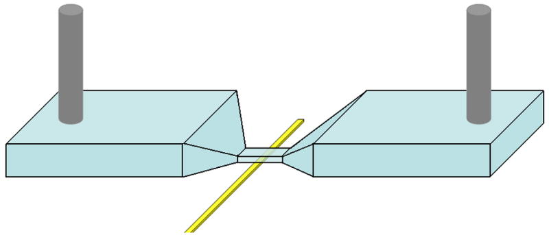
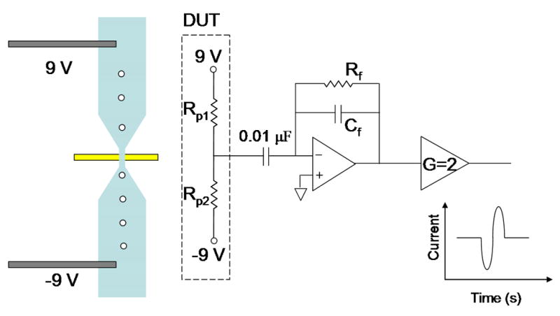
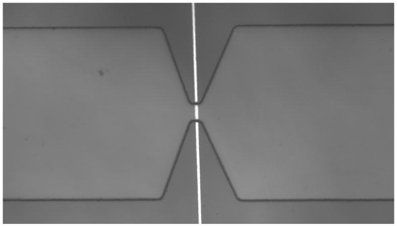
(a) Schematic of microfluidic device integrated with open circuit electrode at the bottom surface of the micropore. Microchannels 300 μm wide taper down to smaller pore so that majority of voltage drop is across the pore. Positive and negative voltage applied at outer channel edges. (b) Circuit diagram of device under test (DUT) integrated with readout electronics. Transient change in current across the pore is amplified using integrator circuit configuration. (Inset) Bead passing through the pore results results in drop in current and then rise. (c) Optical micrograph of fabricated microdevice. Electrode is fabricated on glass substrate. Microchannel on top is embedded in PDMS.
Platinum wires, one tied to 9 and the other tied to -9 V were immersed into the inlet and outlet wells. In addition to the platinum wires on the microfluidic chip, the amplifiers on the circuit board were powered with 9 V batteries. Furthermore, both the microfluidic chip and the printed circuit board (PCB) were housed in a faraday cage, which was a small copper box, in order to shield the measurement electronics from parasitic external electromagnetic interferences. The use of batteries in our setup offered two major advantages. The first advantage was the fact that powering the readout circuitry along with generating sufficient voltage across the channel resulted in a less noisy baseline signal as compared to when the circuit and channel were both powered up by external voltage sources. Furthermore, the use of batteries illustrated the potential to fabricate low-power, portable hand held instruments. The output of the amplifier was fed into a data acquisition card (National Instruments, PCI-6120) where the data was analyzed using a virtual instrument (VI) in Labview (National Instruments) on a PC.
Three Electrode Differential Lock-in Measurement Architecture
As illustrated in Figure 2(a), three electrodes A, B, and C are patterned in the microfluidic channel, such that electrode B is positioned within the micropore. The impedance is measured between electrodes A and B (ZAB), and between B and C (ZBC). The difference between these two impedances (i.e. ZAB - ZBC) is then captured, which shows a negative and subsequently a positive peak, as each particle passes through the pore. This approach is advantageous to a standard two electrode lock-in measurement in that each event (particle passing through pore) results in a unique signature (negative peak followed by positive peak) which can itself be used to further increase the signal to noise ratio using a matched filter, when post processing the data.
Figure 2.
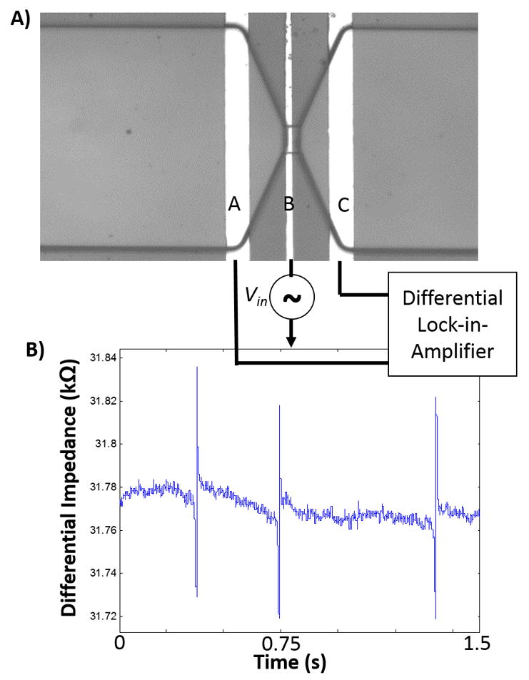
(a) Schematic of three-electrode system with differential lock-in measurement setup. (b) Representative data of measured differential impedance for five beads passing through pore one by one, indicating negative-positive peak signature(PBS used as buffer solution, conductivity ~ 1 S/m).
To perform this measurement we used a lock-in-amplifier (Zurich Instruments, Zurich, CH) where we apply an AC excitation voltage to electrode B, and we attach each of the electrodes A and C to a separate current preamplifier. The outputs of the two current preamplifiers are then tied to a differential amplifier, which then further amplifies the difference by a gain factor (G), the output of which is applied to an amplitude demodulator, consisting of a mixer which shifts the signal back down to baseband in the frequency domain and a low pass filter. The amplitude demodulator essentially serves as a peak detector circuit.
Contactless Impedance Cytometer
Micro-electro cytometers are advantageous to their optical counterparts in that the instrumentation required to perform the readout is significantly lower in cost. The disadvantage, however, is that electrical cytometers require patterning of electrodes on the substrate which results in higher cost of the consumable (disposable) component of the assay compared to optical assays which do not require any micro-patterning on the glass substrate since the measurement can be performed in a contactless format.
Here, we also implement an impedance cytometer where the measurement is performed in a contactless format (Figure 3). With this approach, the electrodes are deposited onto a PCB substrate which is the reusable component, and the disposable unit consists of a thin bare dielectric substrate bonded to a PDMS substrate with a channel embedded into it. The disposable microfluidic channel is placed onto the PCB where the electrodes measure the impedance across the microchannel in a contactless format without becoming contaminated. The microchannel can then be disposed of. The cost of the disposable unit here is significantly cheaper than the disposable unit in a traditional micro-electrode impedance cytometer since no electrode patterning is required. The impedance is measured between the two electrodes using a lock-in amplification measurement, as described before. We previously implemented contactless sensing and demonstrated proof of concept where the base dielectric substrate was a 130 μm thick glass coverslip.3 Here, we present two novel methods for fabricating the contactless device, thus lowering the cost and improving sensitivity. The first involves bonding the top PDMS substrate (with embedded channel) to a thin PDMS membrane, and then placing the chip onto a PCB. The second involves bonding the top PDMS substrate (with embedded channel) to a piece of double-sided tape, which then is placed onto the PCB.
Figure 3.
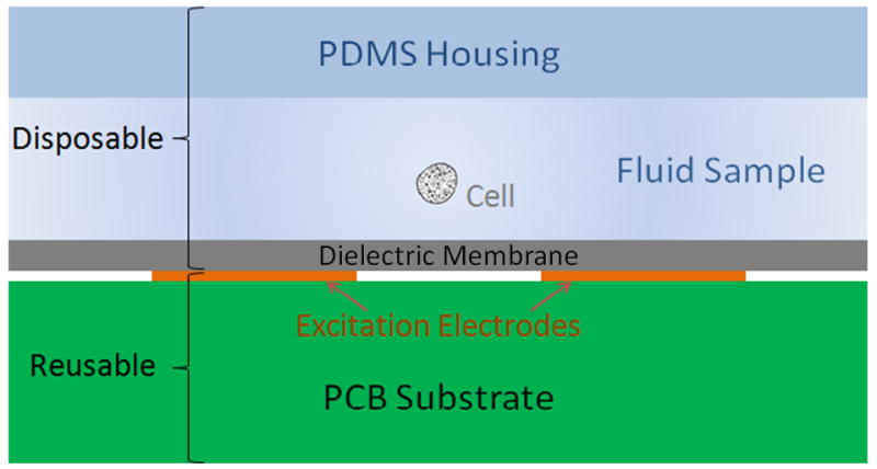
Schematic of contactless impedance cytometer with disposable unit on top of the reusable PCB containing the electrodes.
Fabrication Procedure
Electrode Fabrication for Open Circuit Electrode and Differential Impedance Cytometer
The same fabrication methodology was used to fabricate both the open circuit electrode and the differential impedance cytometer. The microfluidic sensor was fabricated in a two-step manner. The microelectrodes for both the open circuit electrode architecture and also the three electrode architecture were patterned on glass using standard photolithography, evaporation, and liftoff processing.
Microchannel Fabrication
The microchannels for all three architectures was patterned using soft-lithography and imprinted into a PDMS chip. Before the bonding step, 3 mm holes were punched through the PDMS to make inlet and outlet wells. Both the PDMS and glass substrates were treated with oxygen plasma and then aligned and bonded covalently to the glass substrate. Purified DI water was injected into the inlet well using a pipette to keep the channel wet to prevent it from becoming hydrophobic. Given that the PDMS was hydrophilic due to the oxygen plasma bonding treatment, the fluid was wicked so that the microfluidic channel became filled completely with fluid.
Fabrication Method for Contactless Impedance Cytometer
The custom PCB (Sierra Circuits Inc., CA, USA) consisted of 2 mm × 5 mm electrodes spaced 2 mm apart with traces leading from the electrodes to SMA RF connectors on each end. Before each set of measurements, the microchannel pre-bonded onto the desired dielectric layer using the methods described in the next two paragraphs. The bonded chip is aligned and sealed contact with the electrodes using high vacuum grease.
The first method for fabricating the electrodeless sealed microfluidic chip involves bonding the top pdms channel chip onto a thin PDMS membrane. A thin 10 um film of PDMS is spin-coated onto a silicon wafer and then cured, which serves as structural support for the membrane. The PDMS channel chip and the thin membrane are then treated with oxygen plasma, and bonded to each other. An exacto knife is then used to cut through the membrane surrounding the chip, and the chip (bonded to the membrane) is transferred to be placed onto the PCB.
The second method for fabricating the electrodeless sealed micrfluidic chip is similar to the first with the difference that the top PDMS layer is sealed from the bottom with a piece of double sided tape. The electrodelessmicroluidic chip is then taped down onto the PCB for performing measurements.
Sample Preparation and Microchannel Flow
Experiments on the three different architectures were performed using three different particle types: 9 μm polystyrene beads (SpherotechInc, Indianapolis, In), and 2.8 μm paramagnetic beads (Invitrogen Inc.). In these experiments, the beads were suspended in DI water (with conductivity ~ 1 mS) and Phosphate Buffer Saline (PBS, with conductivity ~ 1 S). Sample was pipetted into the inlet well and gravity based flow was used to move the beads/cells through the pore based on the difference in height between the inlet and outlet well. This was the most suitable method for actuating flow in the microdevice in order to obviate the need for tubing and syringe pumps, which also resulted in bringing parasitic noise from the power line into the system, and increased the complexity of the setup.
Results and Discussion
Single Open Circuit Electrode Architecture
Results in Figure 4(a) show electrical pulses resulting from individual beads passing through the pore demonstrating real time detection. Variations in the magnitude of the pulses were observed and are due to beads travelling off of the pore axis. This is a commonly observed effect in coulter counter devices, such as that reported by Saleh et. al.51 Aggregation of beads and the varying number of aggregates also results in variations in the peak magnitudedue to the larger combined volume. Figure 4(b) shows a zoomed in pulse of a single event. The misalignment of the electrode with the pore resulted in asymmetry of the negative and positive peaks, due to the fact that the values for Rp1 and Rp2 are no longer equal.
Figure 4.
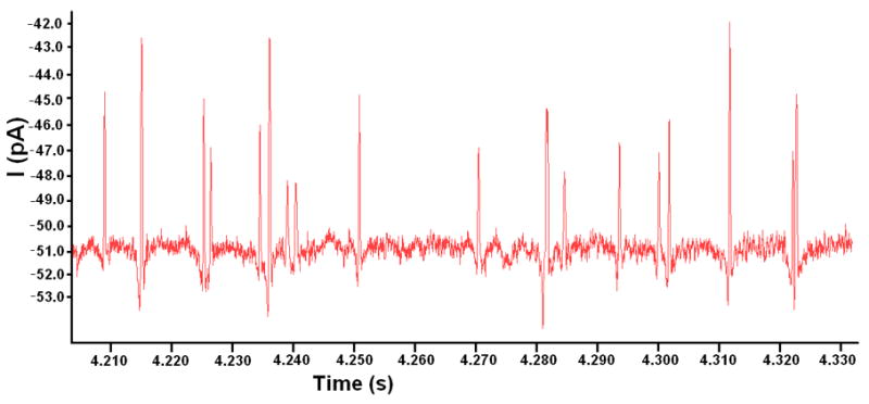
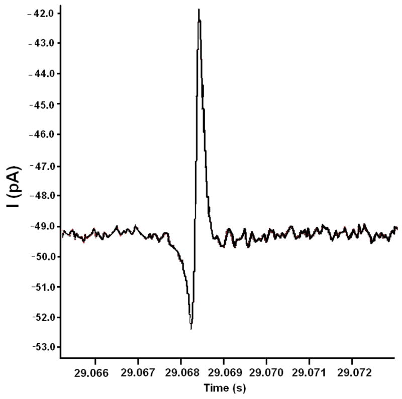
(a) Representative data of current readout for 7 μm diameter beads flowing through the micropore for single electrode open circuit sensing architecture. Peaks of various sizes result from single beads and bead aggregates of varying numbers flowing through the pore. The asymmetry of the positive and negative peaks for each event is due to beads travelling off axis and also imperfect alignment of the sensing electrode to the center of the pore(with DI water as buffer solution). (b) Zoomed in view of representative data of a single bead passing through the micropore.
We performed several control experiments to verify that the observed pulses were indeed due to beads passing through the pore. The first control experiment was an empty device with no fluid to ensure that the sensing electrode was not picking up any spurious signals. The second control experiment was a channel filled with water and no beads injected, and no 9V and -9 V DC voltage being applied at the inlet and outlet of the channel. The third control experiment was similar to the first control experiment, with the difference that the 9 V and -9 V DC voltage was applied at the inlet and outlet of the channel. The fourth and final control experiment was a channel filled with water where beads were injected and no DC voltage was applied between the Pt electrodes at the inlet and outlet wells to confirm that pulses would be observed as a result of the transient shifts in potential on the sensing electrode rather than detection of charge on the beads or some other type of physical mechanism. The output data from all four of the control experiments exhibited no pulses and no signal beyond the background noise which was on the order of 300 fA of current noise, whereas the smallest peak size observed in the positive experiment was at least 3pA.
Three Electrode Differential Lock-in Architecture
Results in Figure 2(b) show representative data of changes in electrical impedance signals resulting from 2.8 μm beads passing through the 40 μm micropore. Passage of each bead through the pore resulted in the expected signature, i.e. a negative peak followed by a positive peak. In order to verify that the signature peaks are indeed due to bead passage, we monitored the micropore under an optical microscope while performing the electrical measurements. A 1 V AC signal is applied at 500 kHz. The average signal to noise ratio for a single bead passing through the pore is 18 (25.1 dB). We previously used this type of impedance sensor in the context of detecting proteins.52
Contactless Measurement
The major challenge we previouslyhad in the contactless sensing approach is that the 130 μm thick glass coverslip acts as an insulator and makes the coupling of the electrodes to the solution extremely difficult since the electric field gets buried in the insulator and does not reach the electrolyte. We resolved this issue by referring to the circuit model, which consists of a combination of the capacitance (due the presence of the insulator) at each end of the electrode terminal in series with solution resistance, altogether in parallel with a parasitic capacitance as a result of electrodes coupling. In conventional impedance cytometers, where electrodes are in direct contact with the electrolyte, double layer capacitance forms at the electrode-electrolyte interface, and one must apply a high enough frequency to short the double layer capacitance. Similarly, in our contactless system, one must apply a high enough frequency to capacitively couple the electrodes to the solution resistance. Using multi-frequency measurements with the lock-in amplifier, we experimentally determined that a frequency of at least 40 kHz was required to begin observing measurable peaks. The advantage with the architecture we used here was that, for both the thin PDMS membrane and the double-sided tape, the thickness of the dielectric layer is at least one order of magnitude thinner than the glass coverslip, resulting in significantly higher capacitance, which makes capacitive coupling to the glass possible at lower frequencies, and also results in higher signal to noise ratio, while decreasing the device cost.
Experiments were performed using 2.8 μm-diameter magnetic beads. In Figure 5a, we plot the impedance spectrum of the contactless device in order characterize the parasitic behavior and determine the optimal regime for device operation. At frequencies below 100 kHz, the impedance is mostly dominated by the capacitance of the insulator layer (sandwiched between the electrode and buffer solution). At frequencies between 100 kHz to 1 MHz, the impedance is dominated by the bulk solution resistance across the electrolyte. This regime is optimal for measuring the impedance of cells or beads passing across the channel. At frequencies above 1 MHz, again we see a drop in impedance with frequency. This region is dominated by the parasitic capacitance. We injected beads into the channel and performed multi-frequency lock-in measurements (Figure 5b). We show this data both for a single peak vs. time and also the average of an ensemble of peaks at multiple frequencies (Figure 5c). As expected, higher frequency results in higher signal to noise ratio.
Figure 5.
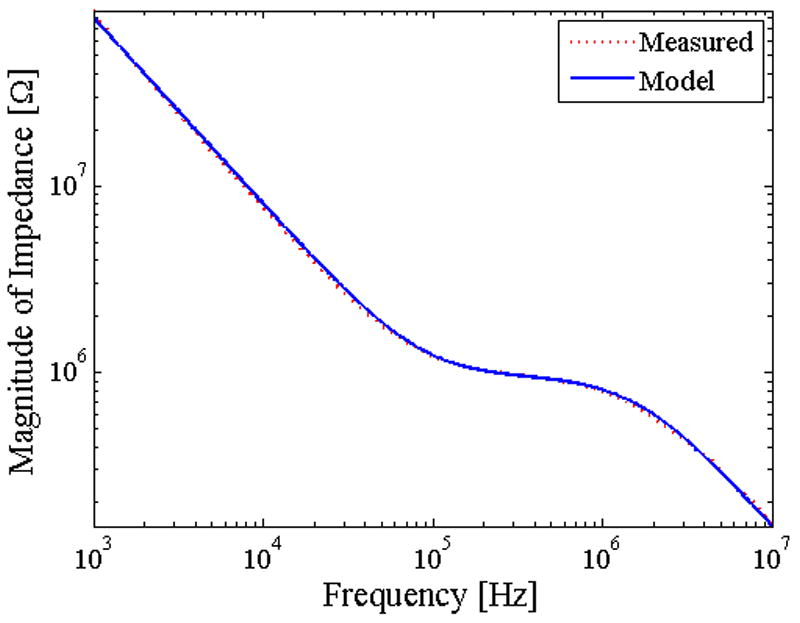
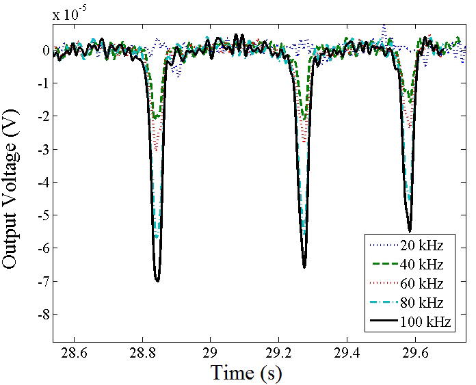
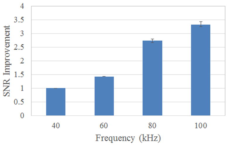
(a) Impedance spectrum of contactless sensor device with PDMS membrane(PBS used as buffer solution, conductivity ~ 1 S/m). (b) Multi-frequency lock-in measurement of contactless measurement system with respect to time (20 kHz was buried in noise). (c) Plot of the average value of the improvement in SNR as a function of frequency.
Conclusion
In conclusion, we have developed three different methods for electronic sensing of cells and micron-sized particles, each geared towards a different application and setting. All three methods have the potential of becoming battery powered. In the first method, we demonstrated a system where the channel excitation and the signal amplification was entirely battery powered. This method used an open-circuit electrode tied to a charge sensitive pre-amplifier, and was based on detecting the shift in potential (which in turn results in transient current changes as observed) when a micron sized particle passes through the pore. The second method was based on a three electrode differential measurement, which opens up the potential of using signal processing techniques to increase signal to noise ratio post measurement. The third architecture used a contactless sensing approach which significantly minimizes the cost of the consumable component of an impedance cytometer. For any of these three architectures, given the robust signal readout, future studies can be dedicated towards integrating both the low noise readout amplification circuitry, along with the analog to digital converter circuitry, and the digital processing unit onto the same chip, thus allowing the whole system to become portable and battery powered. For future work, we will focus on validating these various architectures on clinical blood samples and attempting to characterize electronic cellular properties. This class of devices can find application in low cost cytometry suitable for low resource settings.
Acknowledgments
This work was supported by National Institutes of Health Grant P01 HG000205 and Natural Sciences and Engineering Research Council of Canada Scholarship through graduate tuition support. We would like to thank David Huber, Yang Liu, Robert Dutton, Ronald W. Davis, and Roger Howe for their helpful discussions and advice. We would also like to thank the Stanford Microfluidics Foundry for their help in fabricating microfluidic channel moulds. Electrodes were micropatterned on glass substrates in the Stanford Nanofabrication Facility.
Biographies
Sam Emaminejad received his BASc (2009) and MS (2011) degrees in Electrical Engineering from the University of Waterloo and Stanford University, respectively. He is currently pursuing his PhD in Electrical Engineering at Stanford University, where he is working toward his thesis at the Stanford Genome Technology Center and Stanford School of Medicine. His research is focused on exploiting micro- and nanotechnologies to develop low-cost and integrated biosensing and bioeletronics platforms for personalized medicine applications. Sam has previously worked as an ASIC and Analog Designer in semiconductor companies such as STMicroelectronics and Analog Devices. Sam was awarded Natural Sciences and Engineering Research Council (NSERC) scholarship and was the recipient of Best Paper Award at the IEEE Sensors conference in 2013.
Kee-Hyun Peik is a post-doctoral scholar at Stanford University in the School of Medicine. He received his BS (1998) from Duke University in Electrical Engineering. He received his MS in Electrical Engineering at Stanford University (2001) and in 2012, he received his PhD in Electrical Engineering at Stanford University working on development of nanopore technologies for sensing and fluidic actuation. From 2001 to 2004 he was a development engineer at ISE inc., which is now part of Synopsis. From 2004-2007 he was senior engineer at Samsung Electronics.
Vincent Tabard-Cossa is Assistant Professor in the Physics department at the University of Ottowa. He did his post-doctoral research in the applied biophysics group (Physics) at the University of British-Columbia (UBC), where he studied single-molecule bonds (DNA-DNA for genotyping and receptor-ligand for drug screening applications) using solid-state nanopore-based force spectroscopy (2006-2008). He continued his postdoctoral research at the Genome Technology Center at Stanford University, where he studied the screening behaviour of DNA polymers and fluid transport under high electric fields in nanofluidic transistors (2008-2010). His Ph.D. thesis research was performed in the Scanning Probe Microscopy and Nanoscience group in the Physics Department at McGill University. He investigated the origins of surface stress when various types of molecules trigger chemical/physical reactions at gas-solid and liquid-solid interfaces using AFM-based microcantilever sensors (2000-2005). He received the B.Sc. in Physics from McGill University in the year 2000.
Mehdi Javanmard joined the Electrical and Computer Engineering Department at Rutgers University in Fall 2014 as Assistant Professor. He was a Senior Research Engineer at the Stanford Genome Technology Center (SGTC) in the Department of Biochemistry at Stanford University. He received his BS (2002) from Georgia Institute of Technology where he received the Outstanding Undergraduate Research Award. He received his MS in Electrical Engineering at Stanford University (2004) working at Stanford Linear Accelerator Center researching the use of photonic nanostructures for high energy physics. In 2008, he received his PhD in Electrical Engineering at Stanford University working on development of electronic microfluidic platforms for low cost genomic and proteomic biomarker detection. At SGTC, he worked as a postdoctoral scholar from 2008-2009, and then as a staff engineering research associate from 2009 till 2012. He was recipient of the IEEE Sensors Conference 2013 Best Paper Award. His interests lie in developing rapid and low cost technologies for point-of-care diagnostics, proteomic biomarker discovery, global health, and drug screening.
References
- 1.Saleh OA, Sohn LL. Direct detection of antibody-antigen binding using an on-chip artificial pore. P Natl Acad Sci USA. 2003;100(3):820–824. doi: 10.1073/pnas.0337563100. [DOI] [PMC free article] [PubMed] [Google Scholar]
- 2.Emaminejad S, Javanmard M, Dutton RW, Davis RW. Smart Surfaces: Use of Electrokinetics for Selective Modulation of Biomolecular Affinities. MRS Proceedings. 2012;1415(1) [Google Scholar]
- 3.Emaminejad S, Javanmard M, Dutton RW, Davis RW. Microfluidic diagnostic tool for the developing world: Contactless impedance flow cytometry. Lab Chip. 2012;12(21):4499–4507. doi: 10.1039/c2lc40759k. [DOI] [PMC free article] [PubMed] [Google Scholar]
- 4.Emaminejad S, Javanmard M, Dutton RW, Davis RW. Smart Surface for Elution of Protein Protein Bound Particles: Nanonewton Dielectrophoretic Forces Using Atomic Layer Deposited Oxides. Anal Chem. 2012;84(24):10793–10801. doi: 10.1021/ac302857z. [DOI] [PMC free article] [PubMed] [Google Scholar]
- 5.Javanmard M, Emaminejad S, Dutton RW, Davis RW. Use of negative dielectrophoresis for selective elution of protein-bound particles. Anal Chem. 2012;84(3):1432–1438. doi: 10.1021/ac202508u. [DOI] [PMC free article] [PubMed] [Google Scholar]
- 6.Javanmard M, Davis RW. A microfluidic platform for electrical detection of DNA hybridization. Sensor Actuat B-Chem. 2011;154(1):22–27. doi: 10.1016/j.snb.2010.03.067. [DOI] [PMC free article] [PubMed] [Google Scholar]
- 7.Cheung K, Gawad S, Renaud P. Impedance spectroscopy flow cytometry: On-chip label-free cell differentiation. Cytom Part A. 2005;65A(2):124–132. doi: 10.1002/cyto.a.20141. [DOI] [PubMed] [Google Scholar]
- 8.Gawad S, Cheung K, Seger U, Bertsch A, Renaud P. Dielectric spectroscopy in a micromachined flow cytometer: theoretical and practical considerations. Lab Chip. 2004;4(3):241–251. doi: 10.1039/b313761a. [DOI] [PubMed] [Google Scholar]
- 9.Gawad S, Schild L, Renaud P. Micromachined impedance spectroscopy flow cytometer for cell analysis and particle sizing. Lab Chip. 2001;1(1):76–82. doi: 10.1039/b103933b. [DOI] [PubMed] [Google Scholar]
- 10.Seger U, Gawad S, Johann R, Bertsch A, Renaud P. Cell immersion and cell dipping in microfluidic devices. Lab Chip. 2004;4(2):148–151. doi: 10.1039/b311210a. [DOI] [PubMed] [Google Scholar]
- 11.Scott J, Haber E, Khaw BA. Quantitation of Cell Injury by Fluorescent-Activated Cell Sorting of Antimyosin Coated Myocytes. Circulation. 1981;64(4):154–154. [Google Scholar]
- 12.Thudium DT, Lynch KM, Stewart TT, Narayanan PK, Sellers TS, Schwartz LW. Mulitplexed mouse cytokine measurement using microsphere-based flow cytometry on the Luminex 100. Blood. 2000;96(11):156b–156b. [Google Scholar]
- 13.Balakrishnan P, Dunne M, Kumarasamy N, Crowe S, Subbulakshmi G, Ganesh AK, Cecelia AJ, Roth P, Mayer KH, Thyagarajan SP, Solomon S. An inexpensive, simple, and manual method of CD4 T-cell quantitation in HIV-infected individuals for use in developing countries. Jaids-J Acq Imm Def. 2004;36(5):1006–1010. doi: 10.1097/00126334-200408150-00002. [DOI] [PubMed] [Google Scholar]
- 14.Martin DJ, Sim JGM, Sole GJ, Rymer L, Shalekoff S, Vanniekerk ABN, Becker P, Weilbach CN, Iwanik J, Keddy K, Miller GB, Ozbay B, Ryan A, Viscovic T, Woolf M. Cd4+ Lymphocyte Count in African Patients Co-Infected with Hiv and Tuberculosis. J Acq Immun Def Synd. 1995;8(4):386–391. [PubMed] [Google Scholar]
- 15.McKenzie FE, Prudhomme WA, Magill AJ, Forney JR, Permpanich B, Lucas C, Gasser RA, Wongsrichanalai C. White blood cell counts and malaria. J Infect Dis. 2005192(2):323–330. doi: 10.1086/431152. [DOI] [PMC free article] [PubMed] [Google Scholar]
- 16.Hoerning A, Koss K, Datta D, Boneschansker L, Jones CN, Wong IY, Irimia D, Calzadilla K, Benitez F, Hoyer PF, Harmon WE, Briscoe DM. Subsets of human CD4(+) regulatory T cells express the peripheral homing receptor CXCR3. Eur J Immunol. 2011;41(8):2291–2302. doi: 10.1002/eji.201041095. [DOI] [PMC free article] [PubMed] [Google Scholar]
- 17.Cheng XH, Irimia D, Dixon M, Ziperstein JC, Demirci U, Zamir L, Tompkins RG, Toner M, Rodriguez WR. A microchip approach for practical label-free CD4+ T-cell counting of HIV-infected subjects in resource-poor settings. Jaids-J Acq Imm Def. 2007;45(3):257–261. doi: 10.1097/QAI.0b013e3180500303. [DOI] [PubMed] [Google Scholar]
- 18.Cheng XH, Irimia D, Dixon M, Sekine K, Demirci U, Zamir L, Tompkins RG, Rodriguez W, Toner M. A microfluidic device for practical label-free CD4+T cell counting of HIV-infected subjects. Lab Chip. 2007;7(2):170–178. doi: 10.1039/b612966h. [DOI] [PMC free article] [PubMed] [Google Scholar]
- 19.Esfandyarpour R, Esfandyarpour H, Javanmard M, Harris JS, Davis RW. Electrical Detection of Protein Biomarkers Using Nanoneedle Biosensors. MRS Proceedings. 2012;1414(1) [Google Scholar]
- 20.Esfandyarpour R, Esfandyarpour H, Javanmard M, Harris JS, Davis RW. Microneedle biosensor: A method for direct label-free real time protein detection. Sensors and Actuators B: Chemical. 2013;177:848–855. doi: 10.1016/j.snb.2012.11.064. [DOI] [PMC free article] [PubMed] [Google Scholar]
- 21.Esfandyarpour R, Javanmard M, Koochak Z, Esfandyarpour H, Harris JS, Davis RW. Thin Film Nanoelectronic Probe for Protein Detection. MRS Proceedings. 2013;1572 mrss13-1572-ss01-10. [Google Scholar]
- 22.Esfandyarpour R, Javanmard M, Koochak Z, Esfandyarpour H, Harris JS, Davis RW. Label-free electronic probing of nucleic acids and proteins at the nanoscale using the nanoneedle biosensor. Biomicrofluidics. 2013;7:044114. doi: 10.1063/1.4817771. [DOI] [PMC free article] [PubMed] [Google Scholar]
- 23.Biener G, Greenbaum A, Isikman SO, Lee K, Tseng D, Ozcan A. Combined reflection and transmission microscope for telemedicine applications in field settings. Lab Chip. 2011;11(16):2738–2743. doi: 10.1039/c1lc20169g. [DOI] [PMC free article] [PubMed] [Google Scholar]
- 24.Isikman SO, Bishara W, Mudanyali O, Sencan I, Su TW, Tseng DK, Yaglidere O, Sikora U, Ozcan A. Lensfree On-Chip Microscopy and Tomography for Biomedical Applications. Ieee J Sel Top Quant. 2012;18(3):1059–1072. doi: 10.1109/JSTQE.2011.2161460. [DOI] [PMC free article] [PubMed] [Google Scholar]
- 25.Bishara W, Isikman SO, Ozcan A. Lensfree Optofluidic Microscopy and Tomography. Ann Biomed Eng. 2012;40(2):251–262. doi: 10.1007/s10439-011-0385-3. [DOI] [PubMed] [Google Scholar]
- 26.Mudanyali O, Tseng D, Oh C, Isikman SO, Sencan I, Bishara W, Oztoprak C, Seo S, Khademhosseini B, Ozcan A. Compact, light-weight and cost-effective microscope based on lensless incoherent holography for telemedicine applications. Lab on a Chip. 2010;10(11):1417–1428. doi: 10.1039/c000453g. [DOI] [PMC free article] [PubMed] [Google Scholar]
- 27.Tseng D, Mudanyali O, Oztoprak C, Isikman SO, Sencan I, Yaglidere O, Ozcan A. Lensfree microscopy on a cellphone. Lab Chip. 2010;10(14):1787–1792. doi: 10.1039/c003477k. [DOI] [PMC free article] [PubMed] [Google Scholar]
- 28.Google Patents. Means for counting particles suspended in a fluid. 1953
- 29.Sun T, Gawad S, Green NG, Morgan H. Dielectric spectroscopy of single cells: time domain analysis using Maxwell's mixture equation. J Phys D Appl Phys. 2007;40(1):1–8. [Google Scholar]
- 30.Morgan H, Sun T, Holmes D, Gawad S, Green NG. Single cell dielectric spectroscopy. J Phys D Appl Phys. 2007;40(1):61–70. [Google Scholar]
- 31.Saleh OA, Sohn LL. A chemically sensitive microfabricated resistive pulse analyzer. Biophys J. 2003;84(2):293a–293a. [Google Scholar]
- 32.Saleh OA, Sohn LL. An artificial nanopore for molecular sensing. Nano Lett. 2003;3(1):37–38. [Google Scholar]
- 33.Saleh OA, Sohn LL. Binding assays and single molecule sensing using precision chip-based resistive sensing. Biophys J. 2002;82(1):166a–166a. [Google Scholar]
- 34.Saleh OA, Sohn LL. Quantitative sensing of nanoscale colloids using a microchip Coulter counter. Rev Sci Instrum. 2001;72(12):4449–4451. [Google Scholar]
- 35.Saleh OA, Sohn LL. A resistive sensing device for biological solutions. Biophys J. 2001;80(1):143a–143a. [Google Scholar]
- 36.Sohn LL, Saleh OA, Facer GR, Beavis AJ, Allan RS, Notterman DA. Capacitance cytometry: Measuring biological cells one-by-one. Biophys J. 2001;80(1):144a–144a. doi: 10.1073/pnas.200361297. [DOI] [PMC free article] [PubMed] [Google Scholar]
- 37.Sohn LL, Saleh OA, Facer GR, Beavis AJ, Allan RS, Notterman DA. Capacitance cytometry: Measuring biological cells one by one. P Natl Acad Sci USA. 2000;97(20):10687–10690. doi: 10.1073/pnas.200361297. [DOI] [PMC free article] [PubMed] [Google Scholar]
- 38.Zhu F, Baker D, Skommer J, Sewell M, Wlodkowic D. Real-time 2D visualization of metabolic activities in zebrafish embryos using a microfluidic technology. Cytom Part A. 2015;87(5):446–450. doi: 10.1002/cyto.a.22662. [DOI] [PubMed] [Google Scholar]
- 39.Wlodkowic D, Skommer J, Akagi J, Fujimura Y, Takeda K. Multiparameter Analysis of Apoptosis Using Lab-on-a-Chip Flow. Cytometry Current Protocols in Cytometry. 2013:9.42. 1–9.42. 15. doi: 10.1002/0471142956.cy0942s66. [DOI] [PubMed] [Google Scholar]
- 40.Akagi J, Zhu F, Hall CJ, Crosier KE, Crosier PS, Wlodkowic D. Integrated chip-based physiometer for automated fish embryo toxicity biotests in pharmaceutical screening and ecotoxicology. Cytom Part A. 201485(6):537–547. doi: 10.1002/cyto.a.22464. [DOI] [PubMed] [Google Scholar]
- 41.Thomas RA, Krishan A, Robinson DM, Sams C, Costa F. NASA/American Cancer Society high-resolution flow cytometry project-I. Cytometry. 2001;43(1):2–11. doi: 10.1002/1097-0320(20010101)43:1<2::aid-cyto1012>3.0.co;2-j. [DOI] [PubMed] [Google Scholar]
- 42.Wang L, Flanagan LA, Jeon NL, Monuki E, Lee AP. Dielectrophoresis switching with vertical sidewall electrodes for microfluidic flow cytometry. Lab Chip. 2007;7(9):1114–1120. doi: 10.1039/b705386j. [DOI] [PMC free article] [PubMed] [Google Scholar]
- 43.Wu XD, Kang YJ, Wang YN, Xu DY, Li DY, Li DQ. Microfluidic differential resistive pulse sensors. Electrophoresis. 2008;29(13):2754–2759. doi: 10.1002/elps.200700912. [DOI] [PubMed] [Google Scholar]
- 44.Jagtiani AV, Sawant R, Zhe J. A label-free high throughput resistive-pulse sensor for simultaneous differentiation and measurement of multiple particle-laden analytes. J Micromech Microeng. 2006;16(8):1530–1539. [Google Scholar]
- 45.Jagtiani AV, Zhe J, Hu J, Carletta J. Detection and counting of micro-scale particles and pollen using a multi-aperture Coulter counter. Meas Sci Technol. 2006;17(7):1706–1714. [Google Scholar]
- 46.Wood DK, Oh SH, Lee SH, Soh HT, Cleland AN. High-bandwidth radio frequency Coulter counter. Appl Phys Lett. 2005;87(18) [Google Scholar]
- 47.Scott R, Sethu P, Harnett CK. Three-dimensional hydrodynamic focusing in a microfluidic Coulter counter. Rev Sci Instrum. 2008;79(4) doi: 10.1063/1.2900010. [DOI] [PubMed] [Google Scholar]
- 48.Segerink LI, Sprenkels AJ, ter Braak PM, Vermes I, van den Berg A. On-chip determination of spermatozoa concentration using electrical impedance measurements. Lab Chip. 2010;10(8):1018–1024. doi: 10.1039/b923970g. [DOI] [PubMed] [Google Scholar]
- 49.Kim KB, Chun H, Kim HC, Chun TD. Red blood cell quantification microfluidic chip using polyelectrolytic gel electrodes. Electrophoresis. 2009;30(9):1464–1469. doi: 10.1002/elps.200800448. [DOI] [PubMed] [Google Scholar]
- 50.Zhe J, Jagtiani A, Dutta P, Hu J, Carletta J. A micromachined high throughput Coulter counter for bioparticle detection and counting. J Micromech Microeng. 2007;17(2):304. [Google Scholar]
- 51.Saleh OA, Sohn LL. Correcting off-axis effects in an on-chip resistive-pulse analyzer. Rev Sci Instrum. 2002;73(12):4396–4398. [Google Scholar]
- 52.Mok J, Mindrinos MN, Davis RW, Javanmard M. Digital microfluidic assay for protein detection. Proceedings of the National Academy of Sciences. 2014;111(6):2110–2115. doi: 10.1073/pnas.1323998111. [DOI] [PMC free article] [PubMed] [Google Scholar]


