Abstract
In this paper, we present an experimental and Monte Carlo investigation of the intrinsic spatial resolution that can be achieved with the intensified electron-multiplying charge-coupled device (I-EMCCD) gamma camera [1]–[4]. This detector has a very low readout noise, an ultra-high spatial resolution and a large active area of ~ 80 mm diameter, which is well-suited for small animal imaging applications. The intrinsic detector resolutions achieved with different scintillators and under different experimental conditions were compared. In this study, the simple centroiding method was compared with two model-fitting approaches for finding the locations of gamma ray interactions. The results from Monte Carlo simulation have demonstrated that with an appropriate detector configuration, it is possible to achieve an intrinsic resolution of ~ 30 µm FWHM for detecting 27–35 keV gamma rays. The I-EMCCD scintillation camera offers a promising candidate for future ultra-high resolution SPECT imaging applications.
Index Terms: Intensified EMCCD camera, pinhole SPECT, ultra-high spatial resolution
I. Introduction
IN recent years, substantial efforts have been made to improve the imaging resolution of SPECT systems dedicated to small lab studies. A review of some recent developments in small animal SPECT instrumentations was given by Meikle [5]. These developments have benefited from recent advances in gamma ray sensor technologies, which include the high resolution CZT focal plane detector developed at the University of Arizona [6], [7], the multi-pixel Hybrid PhotoDiode (M-HPD) developed at CERN [8], [9], the double-sided silicon strip sensors developed by Peterson et al. [10], the silicon drift diode (SDD) array developed by Fiorini et al. [11], [12], the Medipix (2) based hybrid pixel sensors developed at CERN [13], [14], EMCCD based mini gamma camera developed by de Vree et al. [15], Heemskerk et al. [16], Nagarkar et al. [17], [18] and Teo et al. [19], the GEM based photon sensors coupled to scintillation materials [20], [21], the intensified EMCCD cameras developed by Meng et al. [1], [2], the scientific CCD based ultrahigh resolution photon sensors[22], the large area multi-channel plate (MCP) based detectors [23], [24], the avalanche photodiode (APD) detectors reported by Yatsu et al. [25] and Shah et al. [26], and the solid-state photomultiplier (SSPM) reported by Stapels [27] etc. Some of these developments have pushed the intrinsic detector resolution to well below a hundred micrometers for detecting 27–140 keV gamma rays. Several groups have proposed or developed prototype SPECT systems that have the potential of achieving an ultra-high imaging resolution in a few hundred microns range. These include the SemiSPECT reported by Kastis [6], the SiliSPECT under development by Peterson et al. [10], the MediSPECT proposed (and evaluated) by Accorsi et al. [28], [29], the U-SPECT-III proposed by Beekman et al. [30], and a low-cost and ultra-high resolution imager based on the second generation image intensifier [31] etc. In addition, Abbott et al. has reported the use of a pre-existing SPECT camera, arranged in an extreme focusing geometry for ultra-high resolution small animal SPECT imaging applications [32].
We have previously proposed to use the intensified EMCCD camera for ultra-high resolution gamma ray imaging applications [1]. A prototype SPECT system was constructed based on this detector and an excellent imaging performance was demonstrated using this system, which includes an intrinsic spatial resolution of ~ 60 µm and an ultra-high spatial resolution in phantom studies [3], [4]. Based on these results, we are currently developing a 4-headed single photon emission microscope (SPEM) system for mouse brain studies. The design and feasibility of the SPEM system were presented in [4], [33]. In addition, we are actively working on an improved I-EMCCD detector that incorporates several modifications (as outlined in Section II-E). In this work, we focused on the intrinsic resolution of the I-EMCCD camera that can be achieved with different scintillators, photo-counting algorithms and detector operating conditions. These results helped us to determine the configuration of the new I-EMCCD detector under development.
II. Material and Methods
A. The Intensified EMCCD Camera
The I-EMCCD detector consists of a columnar CsI(Tl) scintillator, an electron multiplying charge-coupled device (EMCCD) sensor and an electrostatically focused demagnifier tube (http://www.photek.com/phoprodf3.htm). The EMCCD is similar, in structure, to conventional CCDs except that a series of multiplying registers are added before the readout amplifier. These multiplying registers amplify the charge signal by a factor of up to several thousands using the phenomena called “impact ionization” [34]–[36]. This effectively minimizes the readout electronic noise associated with conventional CCDs (especially with fast-scan CCDs). As a result, EMCCDs can offer a readout rate of up to 20 MHz, whilst having an effective readout noise of a few electrons RMS per pixel. In comparison, standard CCDs at similar readout rates would have a readout noise of 30 electrons or more. The performances of several EMCCD-based scintillation gamma cameras have been reported in [15]–[19]. In these gamma cameras, optical fiber-tapers or lenses were used to couple scintillation photons into the EMCCD sensor. For taper-coupled cameras, the relatively low coupling efficiency limits the de-magnification ratio of the taper that can be used. Although an excellent imaging resolution has been demonstrated for detecting low-energy gamma rays (27–35 keV), fiber-coupled EMCCD scintillation cameras (designed for SPECT applications) are currently limited to ≤ 2.4 cm × 2.4 cm in size for use in I-125 imaging applications [18], [19].
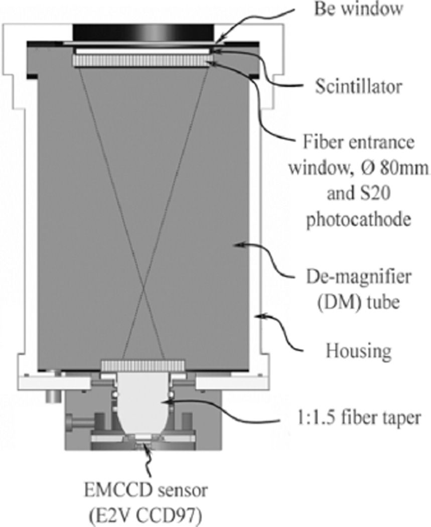
In I-EMCCD, the de-magnifier (DM) tube serves both as an extra gain stage and as an “electronic taper” for enlarging the active area of the camera. The DM tube currently in use has an input window of 80 mm in diameter and an output window of 40 mm diameter. The output is coupled to the EMCCD sensor through a fiber-taper and a fiber-faceplate that have aspect ratios of 1.5:1 and 1:1 respectively. A schematic of the gamma camera is shown in Fig. 1. Detailed discussions on the detector, including its physical configuration and operating characteristic, were previously presented in [1]. For SPECT applications, the current I-EMCCD camera offers the combination of an excellent spatial resolution, a good signal-to-noise ratio (SNR), a large active area (~ 80 mm in diameter), a reasonable detection efficiency, and a simple readout scheme. Although the addition of the DM tube doubled the cost of the entire detector ($25k to $50k), this is offset by a greatly increased active area (from 1.44 cm2 to 50 cm2), which results in a cost-to-area ratio of ~$1000 per cm2. This configuration allows us to use four EMCCD sensors to readout a total imaging area of ~ 200 cm2. This provides a practical solution for constructing an ultra-high resolution SPECT system dedicated for mouse brain studies.
Fig. 1.
The prototype ultra-high resolution gamma camera based on an EMCCD sensor and a DM tube.
B. Estimation of Photoelectron Yield
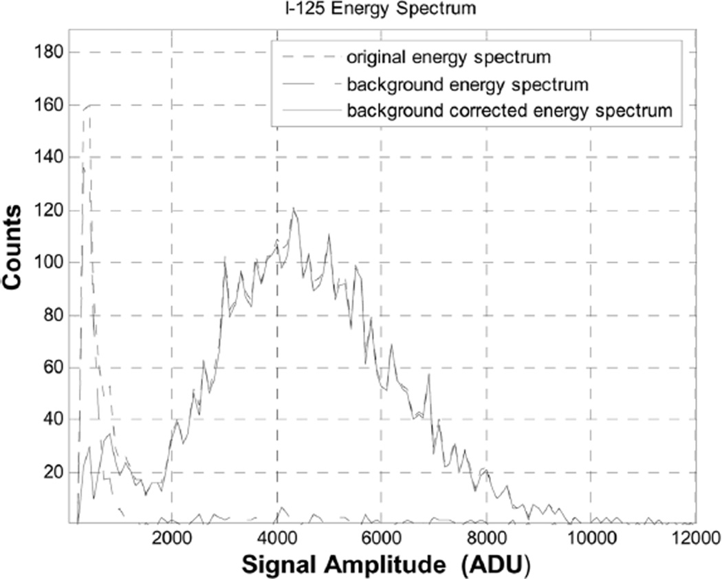
In this study, an indirect approach was used to estimate the number of photoelectrons created (on the DM tube photocathode) by a given energy deposition in scintillator. We have previously measured the light yield of a 200 µm CsI(Tl) phosphor (also procured from Hamamatsu) using a single pixel hybrid photodiode (HPD) [37]. Due to their use of a single gain stage, HPDs are superior to conventional photomultipliers (PMTs) by offering a greatly reduced readout noise. These detectors have an excellent single-photoelectron resolution. It can be used to measure the light yield of scintillators in terms of the number of photoelectrons (p.e.s) generated on the photocathode. The HPD device used has a S-20 photocathode that is deposited on a quartz entrance window. It offers an overall quantum efficiency (QE) of 16% at 500 nm and 9% at 600 nm [38]. In this measurement, 40–50 photoelectrons (p.e.s) were produced on the HPD photocathode by each 59keV full energy event. In comparison, the DM tube, used in the current I-EMCCD camera, has a similar S20 photocathode but optimized for low thermal noise. It has a relatively low QE of ~ 7%. If we assume that the overall QE of the HPD is ~ 10% for CsI(Tl) and the light yield of the 200 µm thick columnar CsI(Tl) scintillator is similar to the 250 µm one used in our measurement, the expected photoelectron yield on the I-EMCCD camera is ~ 13 p.e. per 27 keV energy deposition and ~ 17 p.e. per 35keV. A typical I-125 energy spectrum measured using the I-EMCCD camera and the 250 µm CsI(Tl) scintillator (ACS-HL [39]) is shown in Fig. 2. Based on this discussion, the expected number of p.e.s corresponding to the mean peak position (as shown in Fig. 2) is 13–15 p.e.s. With this information, one can calibrate the I-EMCCD camera for operating at different EM gains. The photoelectron yield of the camera, when used with different scintillators, can be determined accordingly.
Fig. 2.
A measured I-125 energy spectrum. The EM gain used was ′500. A columnar CsI(Tl) scintillator (Hamamatsu, ACS-HL) of 250 µm thick was used. The operating temperature of the EMCCD sensor was −35°C.
C. Experimental Setup
The intrinsic resolution of the I-EMCCD camera was measured using a slit aperture of 25 µm wide, which was made of two tungsten sheets of 500 µm in thickness. The aperture was placed right on top of the scintillator in use. An I-125 source was placed 10 cm away from the aperture. The source was 500 µm in diameter and contains 250 µCi activity. The intrinsic detector resolution was determined in terms of full-width-at-half-maximum (FWHM) and full-width-at-tenth-maximum (FWTM) of the measured line-spread functions (LSF). The effect of the 25 µm slit width was subtracted in quadrature from measured FWHMs and FWTMs. In this measurement, two columnar CsI(Tl) scintillators (ACS-HL type [39]) were used. Their thicknesses were the 250 µm and 500 µm respectively. For each measured EMCCD frame, local maxima were sought as potential interaction positions. For each local maximum, a small region consisting of an array of 7 × 7 pixels was defined around the peak pixel. Gamma interactions are identified based on the use of four threshold values. These are the upper and lower limits for the signal amplitude on the peak pixel and the sum of all signals over the 7 × 7 array. The integrated signal amplitude was used to indicate the energy deposition by a given interaction.
D. Estimation of Interaction Position
In this study, we compared three algorithms for localizing gamma ray interactions in the CsI(Tl) scintillator. A similar comparison was previously presented by Fisher et al.. [40]. The first approach that we used is the simple centroiding method. It was performed over a 7 × 7 array of pixels around the peak pixel. This approach is relatively simple and computationally efficient. It was used as the standard position estimation method for most of our studies.
We also implemented two model-fitting based methods for localizing gamma ray interactions. In these methods, the distribution of scintillation light was modelled as the sum of multiple 2-D Gaussian functions as shown below,
| (1) |
where (x0, y0) is the common center of the distributions. Ai’s and σi’s are the weighting factors and standard deviation values. σsecondary accounts for an extra blurring that is introduced by the fiber faceplate used as the output window of the DM tube. It was assumed to be 20 µm, according to manufacturer’s specification [41].
With the signal model shown in (1), we first implemented the weighted least-square (WLS) method for estimating the interaction position of each event. It finds the interaction location by minimizing the following objective function:
| (2) |
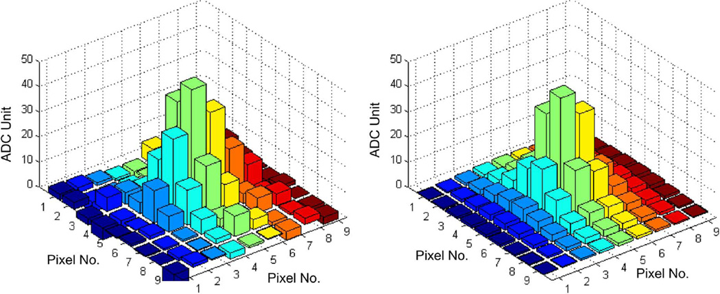
where ni and mi(θ) are the measured and expected signal amplitudes on the i’th pixel. The fitting process was performed using a Matlab code based on the Levenburg-Marquardt algorithm [39]. An example of measured and fitted distribution of signals across EMCCD pixels are shown in Fig. 3. In this case, model (1) consists of two Gaussian components only. All six model parameters in (1) were left free in the actual fitting process.
Fig. 3.
Measured (left) and fitted (right) signal distribution on EMCCD, induced by an I-125 photon interaction in a 500 µm thick columnar CsI(Tl) scintillator. The horizontal axes are EMCCD pixel numbers and the pixel size was 16 µm × 16 µm. The vertical axis is the measured signal amplitude in ADC unit (ADU). A relatively low EM gain of 20 was used in this measurement. The RMS of the distribution (on EMCCD) is ~ 20µm, which is corresponding to ~ 120µm RMS on the photocathode of the DM tube. The total distribution contains ~ 20 photoelectrons, which was derived based on the calibration process described in Section II-B. In this measurement, a single photoelectron is corresponding to roughly 13 ADC units.
For further evaluating model-fitting based methods, we also implemented maximum-likelihood (ML) approach for finding the interaction position. With a sufficient EM gain, the readout amplifier noise is negligible (≪ 1e−/pix). According to manufacturer’s specification [42], the EMCCD dark-count rate (from the clock-induced charge (CIC) [34]) is a few at e−/pixel · s at −35°C. When read out at 30 fps, we expect the dark counts rate to be at the order of 0.1e−/pixel·frame. Since this component is very small compared to the signal induced by a single photoelectron (10e−) and given that scintillation signal is mostly distributed over a small cluster (3 × 3 to 7 × 7) of pixels, the effect of EMCCD dark-count noise is ignored in the simulation. Therefore, the uncertainty on measured signals is dominated by statistical fluctuation that can be modelled with a 2-D Poisson point process [43]. In such case, one can use maximum likelihood (ML) algorithm to find the interaction locations [44], [45]. For each detected event, the likelihood function of the measured signal distribution is given by
| (3) |
where ni’ is the measured number of photoelectrons on the i’th pixel. In this study, the number of photoelectrons per pixel was determined by the calibration process described previously in Section II-B. Interaction locations can be obtained by the following maximization process
| (4) |
In this study, a comparison between the three event-positioning algorithms was performed based on the data acquired under various experimental conditions.
E. Monte Carlo Simulations
The intrinsic resolution of I-EMCCD devices may be further improved by incorporating updated components. These include
A customized DM tube for I-EMCCD applications. We have recently developed (along with Photek Ltd, UK http://www.photek.com/) a new DM tube that incorporates several improvements over the current version. The new DM tube has a photocathode QE of 10–12% rather than the ~ 7% found in our current DM tubes. It also has a variable DM ratio (DMR) that is controlled by a micro-processor and variable from 1:1 to 1:6. When needed, a smaller DM ratio can be used with the current EMCCD sensor, which results in smaller optical pixel sizes (24 µm with DMR = 1 : 1, 48 µm with DMR = 2 : 1) on the photocathode.
High resolution scintillators. An example is the commercially available high resolution columnar CsI(Tl) scintillators on either amorphous-carbon substrate or aluminium substrate (ACS-HR and ALS-HR [39]). These phosphors have a quoted line-pair value that is ~ 50% better than the HL (high light-yield) version scintillators currently in use [39]. It is worth noting that the HR version scintillators have a much lower light yield than that of the corresponding HL version scintillators. However, we expect that the increased QE (from 7% to 12%) on the new DM tube should be sufficient to offset the lowered light yield. In the following simulation, we have used the same photoelectron yield for both HL and HR versions scintillators.
A new mega-pixel EMCCD sensor. The intrinsic resolution of I-EMCCD may also be improved using a new megapixel EMCCD sensor (CCD201–20 by e2V Technologies [46]). It is a back-illuminated sensor with 1k × 1k 13 µm pixels. When incorporated into the I-EMCCD detector, this sensor provides 1k × 1k resolution across the 80 mm diameter active area.
In this study, Monte Carlo simulations were performed to evaluate the intrinsic detector resolution of an I-EMCCD that incorporates these hardware upgrades. For each event, the simulation process consists of the following steps. Step 1: A certain number of photoelectrons are randomly generated on the DM photocathode. These photoelectrons are distributed according to a 2-D Poisson point process that follows the double-Gaussian model (1). Model parameters used in this study were determined based on experimentally measured signal distribution. These photoelectrons are then projected onto a smaller plane, according to the DM ratio used (typically ranging from 2:1 to 6:1). Step 2: for each of these photoelectrons, multiple electrons (on EMCCD sensor) were generated. The number of these electrons follows Poisson distribution having a mean of 10. This reflects the estimated 10 electrons (on EMCCD) per photoelectrons (on DM photocathode) in the current I-EMCCD detectors [1]. The positions of these electrons follow a 2-D Gaussian distribution centered at the original position of the corresponding photoelectron. The Gaussian distribution has a FWHM of 20 µm. This is to account for the resolution of the fiber components between the DM tube and the EMCCD sensor. Step 3: All electrons created are then sampled by a simulated CCD sensor that has square pixels of 16 µm or 8 µm in size. A Gaussian noise of 0.1 electron root-mean square (RMS) was added to the number of electrons collected by each pixel. This models the remaining readout noise of the EMCCD sensor after the electron-multiplying (EM) amplification. Note that the EMCCD gain is not explicitly included. We assumed that that a sufficient EM gain, say greater than 200, is used. Therefore, the fluctuation on the number of electrons collected per pixel is dominated by Poisson noise that is associated with the generation and distribution of photoelectrons and the conversion efficiency from photoelectrons to electrons on EMCCD. The DM gain was fixed by a given 10kV high-voltages as currently in use. Step 4: for each event, the interaction location is derived by centroiding over a 7 × 7 array of pixels that are centered at the pixel with the maximum signal amplitude. A large number of events were generated with this sequence for evaluating the intrinsic resolution.
III. Results
A. Measured Signal-to-Noise Ratio (SNR)
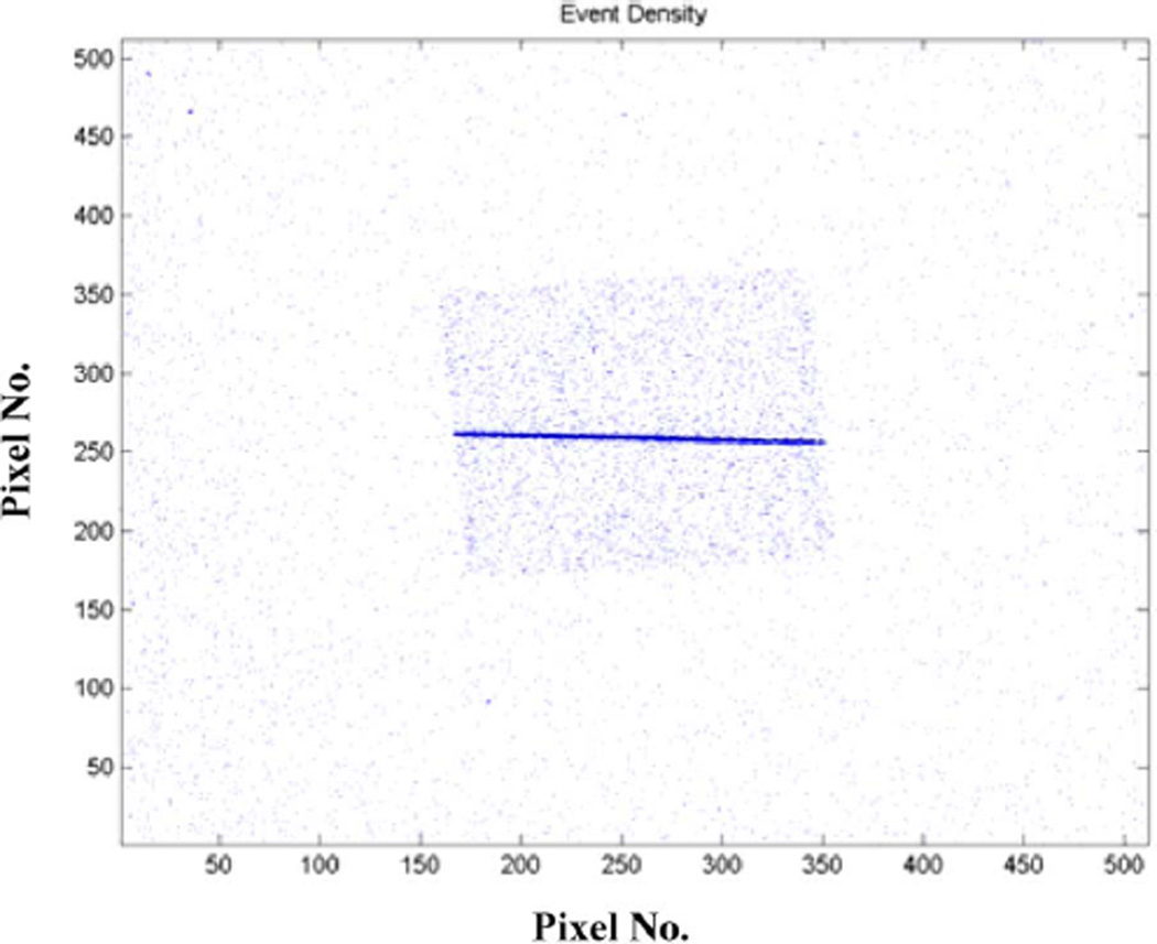
To demonstrate the SNR achievable with the I-EMCCD detector, we have carried out a series of measurements under different experimental conditions. A small piece of CsI(Tl) scintillator, of 1.4 cm × 1.4 cm in size and 250 µm thick, was attached to the I-EMCCD detector. The scintillator covers ~ 1/9 of the active area of the camera. A tungsten slit of ~ 25 µm wide was placed against the scintillator. An I-125 radiation seed with an activity of ~ 150 µCi was placed ~ 10 cm away from the slit. A measured projection of the source on the I-EMCCD/CsI(Tl) setup is shown in Fig. 4. The noise events, in area not covered by the scinitllator, are mostly due to the thermal emission of photoelectrons from the DM photocathode. Similar to true events, these noise events result in clusters of signals that spread over multiple CCD pixels. These events can be (partially) rejected with proper threshold settings. With an energy threshold at 3 photoelectrons, an event rate of a few counts per second over the entire detector can be achieved. This should be sufficiently low for most of SPECT applications.
Fig. 4.
Measured I-125 photon interactions on the I-EMCCD detector coupled to a small piece of CsI(Tl) scintillator of 250mm in thickness. The background events in regions not covered by the scintillator were resulted from the thermal emission of photoelectrons at the DM photocathode.
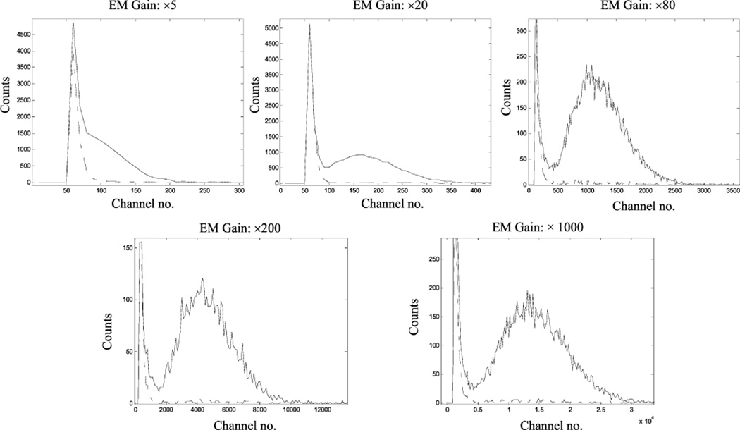
Using this setup, we derived the energy spectra for true I-125 events and background events by choosing interactions from different regions in the projection. I-125 energy spectra measured with different EM gains are compared in Fig. 5. Even with the extra multiplication provided by the DM tube (~ 10), a substantial EM gain was needed for differentiating the true I-125 interactions from the background counts.
Fig. 5.
Measured I-125 energy spectra with different EM gain, ranging from 5 to 1000. The EMCCD camera was cooled to −35°C for these measurements.
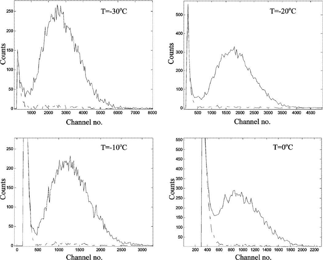
The temperature dependence of SNR of a fiber-coupled EMCCD scintillation detector was previously reported by Heemskerk et al.. [16]. In their measurement, a back-illuminated EMCCD detector (8 mm × 8 mm in size) was coupled to a CsI(Tl) phosphor through an 1:1 fiber-stud. A reasonable energy resolution was demonstrated for detecting I-125 gamma rays even at 0°C. In this study, we carried out a similar measurement using the I-EMCCD camera coupled to a 250 µm thick columnar CsI(Tl) scintillator. Several energy spectra measured at different EMCCD operating temperatures are shown in Fig. 6. The increasing temperature leads to an increased thermal noise count rate that appeared at the low-end of the spectra. Another effect of the increasing temperature is that the photopeak position appears to be shifting towards the low-energy end. This indicates a reduced effective EM gain with increased operation temperature. Note that the gain settings shown in Fig. 6 are based on the relationship between multiplication-voltage and EM gain as suggested by the manufacturer. The actual gain of the sensor is known to drift at different temperatures. According to [42], the gain decreases by a factor of 2 for every 8 degrees increase in temperature. This led to the significant decrease in SNR as observed in Fig. 6. The readout noise level of the amplifier used in the EMCCD sensor may also vary with temperature, but its effect on the overall SNR should be small in comparison to the impact of the decreasing gain. The effect of temperature on detector intrinsic resolution is discussed in Section IV.
Fig. 6.
I-125 energy spectra measnrued at different operating tempertures, ranging from −30 °C to 0 °C. The EM gain used was ′200 for these measurements.
B. Measured Intrinsic Detector Resolution
Three methods for position estimation (as outlined in Section II-D) were compared under a variety of experimental conditions. The results are shown in Tables I–III. In these measurements, an energy threshold of 3 photoelectrons was used. In these comparisons, the simple centroiding method provided the best spatial resolution, although it is the simplest one within the methods compared. ML fitting is a theoretically superior approach. But this did not translate into an improved intrinsic resolution. As we expected, the EM gain plays an important role in detector intrinsic resolution. With an EM gain of greater than 200, the spatial resolution achieved is limited by Poisson fluctuation on the signal (primarily on the quantity and distribution of photoelectrons generated on the DM photocathode). The measured spatial resolution depends only weakly on operating temperature. Therefore, if intrinsic detector resolution is the primary concern and the increased dark count rate is less restrictive, one can operate the camera at 0°C and still achieve an excellent spatial resolution (~ 80 µm FWHM) for detecting X and gamma rays emitted by I-125.
TABLE I.
Measured Intrinsic Spatial Resolution of the I-EMCCD Camera With an Optical Pixel1 Size of 96 mm and an 250 mm Thick CsI(Tl) Scintillator
| EM Gain | WLS | Maximum Likelihood | Centroiding | |||
|---|---|---|---|---|---|---|
| FWHM (µm) | FWTM (µm) | FWHM (µm) | FWTM (µm) | FWHM (µm) | FWTM (µm) | |
| ×1000 | 55.1 | 115.4 | 51.9 | 110.7 | 51.9 | 111.9 |
| ×200 | 58.8 | 116.0 | 60.1 | 119.5 | 56.3 | 110.1 |
| ×20 | 73.0 | 124.2 | 88.7 | 170.4 | 71.2 | 139.5 |
| ×5 | 95.9 | 165.7 | 90.5 | 212.4 | 108.3 | 162.2 |
An optical pixel on the DM photocathode is the maximum area that can be projected onto a single pixel on the EMCCD sensor (16µm×16µm)
TABLE III.
Measured Intrinsic Spatial Resolution1 at Different EMCCD Operating Temperatures
| Temp. | WLS | ML | Centroiding | |||
|---|---|---|---|---|---|---|
| FWHM | FWTM | FWHM | FWTM | FWHM | FWTM | |
| −30C | 53.2 | 112.5 | 55.1 | 120.7 | 50.6 | 106.5 |
| −20C | 62.6 | 127.8 | 65.1 | 135.4 | 58.8 | 121.9 |
| −10C | 63.2 | 127.2 | 72.4 | 155.8 | 57.6 | 116.9 |
| 0C | 86.3 | 134.2 | 89.3 | 191.3 | 80.3 | 141.3 |
An optical pixel size of 96 µm and the 250 µm thick CsI(Tl) scintillator was used in this measurement. The EM gain used was ×200.
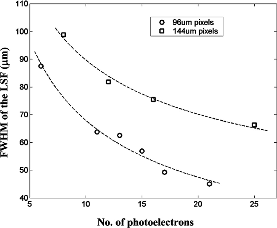
Fig. 7 shows the intrinsic resolution of the I-EMCCD detector as a function of both optical pixel size and the number of photoelectrons. The detector was operated at −30°C with an EM gain of 200. The 250 µm thick ACS-HL scintillator was used for this measurement. Given the 16 µm pixel size on the EMCCD sensor and the fixed 1:1.5 fibre-optic taper between the EMCCD and the DM tube, the optical pixel size on the photocathode was varied by changing the DM ratio (4:1 for 96 µm pixels and 6:1 for 144 µm pixels). The data points shown in Fig. 7 were obtained by selecting events that have their corresponding photoelectron yield falling into different energy bins of 1 photoelectron in width. As shown in Fig. 7, changing the effective optical pixel size from 96 µm to 144 µm resulted in a substantially degraded spatial resolution.
Fig. 7.
Experimentally measured intrinsic resolution with 2 different optical pixle sizes. An optical pixel on the DM photocathode is the maximum area that can be projected onto a single pixel on the EMCCD sensor (16 µm ×16 µm).
C. Measured Signal Distribution
The fitting process for calculating interaction positions also allowed us to quantify the distribution of photoelectrons on the photocathode of the DM tube. Based on the double Gaussian model, we used WLS method to go through a large number (> 10,000) of measured events. The mean and standard deviation of the corresponding model parameters were derived for the 250 µm and 500 µm scintillators as shown in Table IV. Note that given the large sample size (> 10,000), the measured standard deviation on σ was much larger than that predicted by statistical fluctuation. The extra fluctuation may be explained by the fact that interactions occurred at different depths in the scintillator introduce signal distributions of different widths.
TABLE IV.
Measured Model Parameters
| Scintillator | Mean width of individual Gaussian components |
Measured std. dev. on σ |
A1/A2 |
|---|---|---|---|
| 250µm ACS-HL |
σ1=125µm | 27.2 µm | 1.55 |
| σ2=152 µm | 33.2 µm | ||
| 500µm ACS-HL |
σ1=164 µm | 44.2 µm | 1.67 |
| σ2=204µm | 74.4 µm |
D. Monte Carlo Simulations
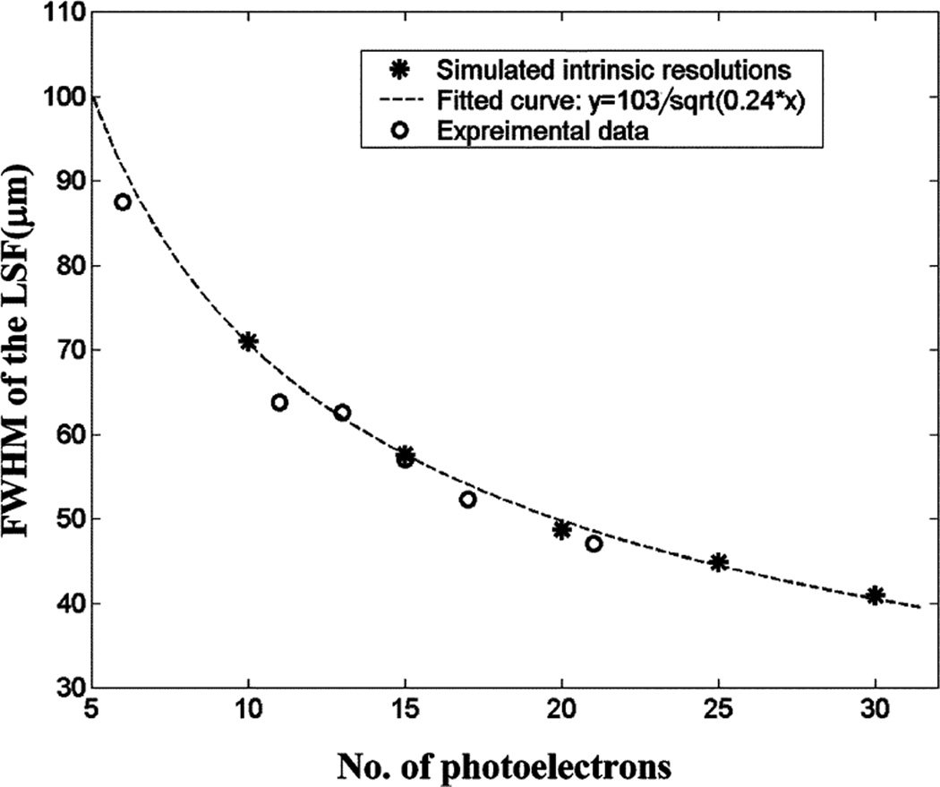
In this study, Monte Carlo simulation was used to predict the intrinsic resolution that can be achieved with several scintillators. To validate the accuracy of this method, simulated detector intrinsic resolution as a function photoelectron yield was compared with measured values in Fig. 8. The 250 µm thick CsI(Tl) ACS-HL was used in this comparison. A reasonable agreement was demonstrated in the comparison. Note that the measured intrinsic resolutions with the optical pixel size of 144 µm are greater than the estimated ones (for example, by 20% with a signal level of 10 p.e.s). Since the photoelectron-yield of the detector was estimated indirectly, it is possible that the number of p.e.s was overestimated. This should partially account for the discrepancy between estimated and measured intrinsic resolutions. This difference may also be explained by the imperfection of the multiple-Gaussian model that was used to describe the distribution of the photoelectron signal. When scintillation photons are traveling in directions parallel to the exiting surface of the scintillator, they suffer more attenuation than photons travelling along the fine columnar structures. Therefore, the actual distribution of photoelectrons along the lateral direction will not have the infinitely long tail as predicted by the Gaussian model (1). In this case, the use of 144 µm pixels may be too large for sampling the photoelectron signals, since the actual distribution has a much faster fall-off than the corresponding Gaussian model. The actual intrinsic resolution will be poorer than that predicted based on the Gaussian model. A smaller pixel size (96 µm or 48 µm) allows a better sampling of the peak area of the distribution. Even though the imperfections of the Gaussian model will still lead to an overestimated intrinsic resolution, its effect will be smaller. Therefore, a better matching between estimated and measured resolutions is shown in the comparison between Figs. 7–9.
Fig. 8.
Comparison between the measured and simulated intrinsic spatial resolution. A 250mm thick ACS-HL scintillator was used in the experiment. The optical pixle size was 96 mm and the EM gain was 200. The centroiding method was used for both MC and experimental data.
Fig. 9.
Simulated intrinsic spatial resolution as a function of the number of photoelectrons. The distribution of the light signal was based on the model derived for the 250 mm thick Hamamatsu ACS-HL scintilaltor. Optical pixel sizes are shown in the figure.
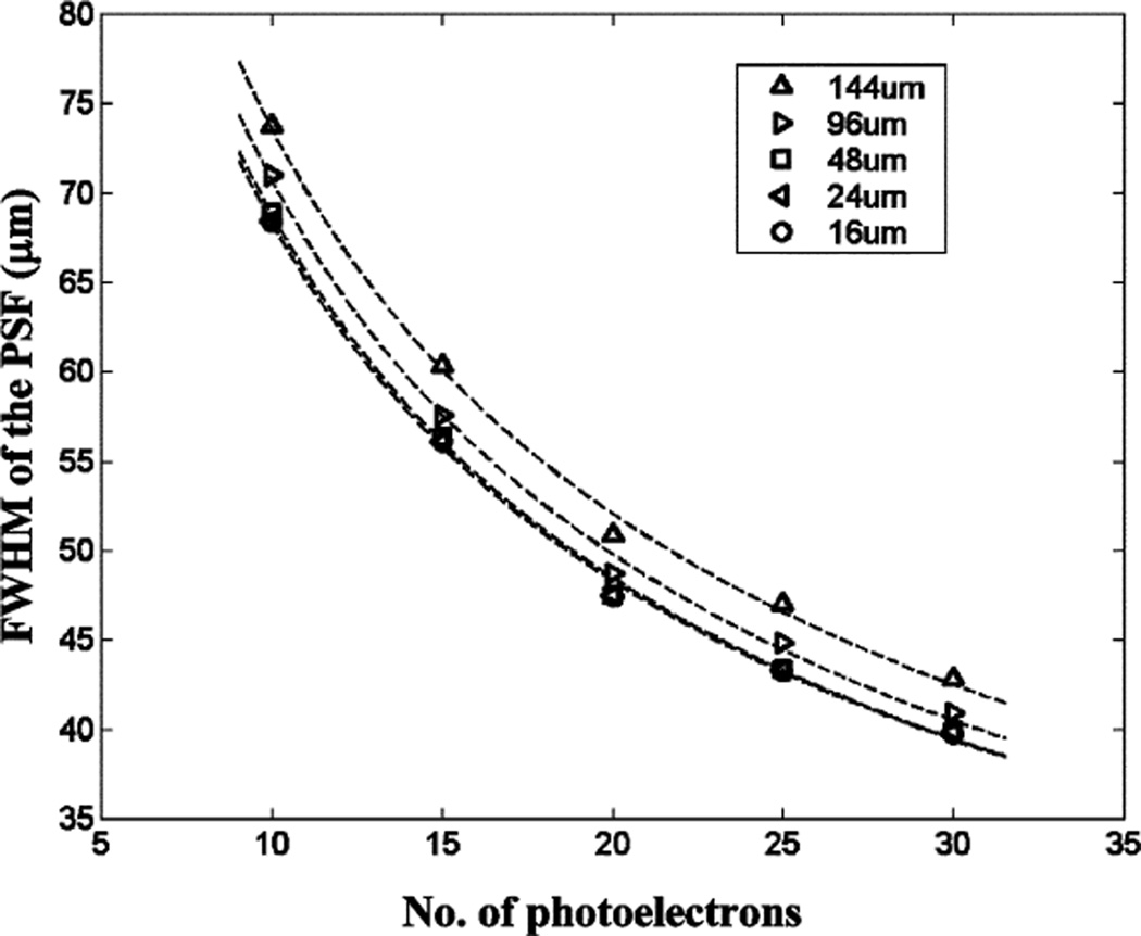
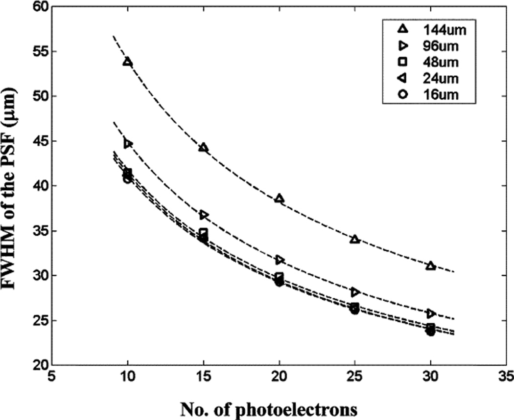
In this study, four scintillators were simulated, with their corresponding model parameters shown in Table IV and Table V. For the HR version scintillators, we assumed that the widths of both Gaussian components are 60% of the corresponding HL scintillators. The simulated intrinsic resolution for the I-EMCCD camera coupled to a 250 µm thick CsI(Tl) scintillator is shown in Figs. 9 and 10. With the ACS-HL scintillator, the best resolution was achieved with a pixel size of 48 µm. The use of the 250 µm HR scintillator can provide a substantially improved resolution. This simulation indicated that intrinsic resolution values, ranging from 40 µm to 22 µm, can be achieved with 48 µm pixels. There is virtually no change in resolution with pixels smaller than 48 µm. In this simulation, an intrinsic resolution of ~ 30 µm has been demonstrated using the 250 µm thick ACS-HR scintillator and an I-EMCCD detector with 48 µm optical pixels.
TABLE V.
Simulated model Parameters for HR Scintillators
| Scintillator | Mean width of individual Gaussian components |
A1/A2 |
|---|---|---|
| 250µm ACS-HR1 |
σ1=75µm | 1.5 |
| σ2=90 µm | ||
| 500µm ACS-HR |
σ1=96µm | 1.6 |
| σ2=120 µm |
The widths of signal distribution for the ACS-HR scintillators are simply scaled down from the corresponding values for the HL version by a factor of 0.6.
Fig. 10.
Simulated intrinsic spatial resolution as a function of the number of photoelectrons. The distribution of the light signal was based on the model derived for the 250 mm thick Hamamatsu ACS-HR (HR stands for high resolution) scintilaltor. Optical pixel sizes are shown in the figure.
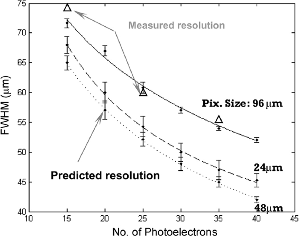
A similar comparison is shown in Fig. 11 for a 500 µm ACS-HL scintillator. The use of 48 µm pixels provided a modestly improved resolution and the use of optical pixel sizes of smaller than 48 µm actually led to a degraded spatial resolution. A simple explanation for this result will be given later in Discussion section. A few experimentally measured resolution values are also shown in the figure for validating these simulation results. Finally, the intrinsic spatial resolutions of the I-EMCCD camera coupled to various scintillators are summarized in Table VI. Unless scintillators with a further reduced light spread (compared to that of the 250 µm ACS-HR) are available, 48 µm pixel size appears to be optimal for improving the spatial resolution. As previously discussed, the 48 µm pixel size can be achieved by coupling the DM tube to the 1k × 1k EMCCD sensor, or using a DM ratio of 2:1 with the current 512 × 512 pixel EMCCD device.
Fig. 11.
Predicted intrinsic spatial resolution of the IEMCCD camera coupled to columnar CsI(Tl) scintillators of 500 µm thickness. Three measured data points are also shown for validating the MC results. An optical pixel size of 96 µm was used in these experiments.
TABLE VI.
Measured and Simulated Detector Intrinsic Spatial Resolution
| EMCCD (# of pixels) |
Scintillator | Readout Frame Rate (fps) |
Optical Pixel Size (µm) |
FWHM (µm) |
FWTM (µm) |
|
|---|---|---|---|---|---|---|
| 512×512 | Gadox, 60µm thick [1] | 32 | 96 | 60 | 123 | Measured |
| 256×256 | Gadox | 54 | 192 | 92 | 190 | Measured |
| 128×128 | Gadox | 95 | 384 | 119 | 227 | Measured |
| 512×512 | Columnar CsI(Tl), 500µm Hamamatsu, ACS-HL |
32 | 96 | 65 | — | Measured |
| 512×512 | Columnar CsI(Tl), 250µm Hamamatsu ACS-HL |
32 | 48 | ~50 | ~112 | Measured |
| 1024×1024 | Columnar CsI(Tl), 500µm Hamamatsu ACS-HR |
10 | 48 | ~561 | ~110 | Simulated |
| 1024×1024 | Columnar CsI(Tl), 250µm Hamamatsu ACS-HR |
10 | 48 | ~301 | ~64 | Simulated |
The overall spatial resolution shown is the simulated value for events that create 20p.e.s on the DM photocathode.
IV. Conclusions and Discussions
EMCCD based scintillation detectors offer an excellent performance for imaging low energy gamma rays. Compared to the fiber-coupled EMCCD scintillation cameras, the major advantage of the scintilaltor/I-EMCCD detector is the capability of achieving excellent intrinsic resolution and SNR over a large active area. It allows one to construct a high performance and practical SPECT system with a small number of EMCCD sensors. This partially offsets the current high cost of EMCCD sensors. In this study, we focused on evaluating the spatial resolution of the detector for imaging low energy gamma rays 27–35 keV energies.
The current I-EMCCD detector with 250 µm and 500 µm thick CsI(Tl) scintillators provided intrinsic resolutions of ranging from 50 µm to 65 µm FWHM. As demonstrated with Monte Carlo simulation, the I-EMCCD detector has the potential of offering ~ 30 µm intrinsic resolution for detecting gamma rays having 27–35 keV energies. This requires the use of high resolution columnar CsI(Tl) scintillators and an effective pixel size of 48 µm on the DM photocathode. The 48 µm pixel size can be achieved with the use of the mega-pixel EMCCD sensor or with a DM tube that has a smaller DM ratio.
For the scintillators studied, the use of optical pixel sizes of smaller than 48 µm offered little or no benefit. In some cases, it led to a degraded spatial resolution. This is evident in Figs. 9–11. This result may be explained with the well-known signal sampling considerations [44]. Given that the signal distribution may be approximated with 2-D Gaussian functions, its Fourier transform is also Gaussian distributed, with the Fourier coefficients decreasing quickly at higher spatial frequencies. In practice, the distribution of scintillation signal on detector may be considered to be band-width limited. Therefore, the sampling frequency defined by detector pixel size should not be much greater than the corresponding Nyquist sampling frequency. Otherwise, excessive readout noise (normally associated with higher spatial frequencies) will be added without real gain in true photoelectron signal. This explains why smaller pixels actually led to worse intrinsic resolution values.
In this study, three methods were evaluated for deriving interaction location. This comparison was based on data sets acquired with different scintillators. For 250 µm and 500 µm thick scintillations used, the simple centroiding method outperformed model-fitting based methods in both resultant intrinsic resolution and simplicity. The current I-EMCCD camera was tested at several operating temperatures. Although a superior performance can be achieved with the EMCCD sensor cooled to −35°C, one may achieve a useful performance even when operating the camera at 0°C, with a detector intrinsic resolution of 80 µm. This results may be compared to the measurements previously reported in [16], which is based on the use of the same EMCCD sensor [46] coupled to columnar CsI(Tl) scintillators through a small fiber stud.
Compared to fiber tapers, the DM tube introduces extra dark counts, mainly through thermal emission of photoelectrons from the photocathode. Further more, the DM tube has a relatively low QE at 500–650 nm wavelength, so that only a small fraction of scintillation photons can be converted to photoelectrons. Despite these factors, the use of the DM tube produced an excellent signal-to-noise ratio for detecting I-125 gamma ray interactions. Another concern of using the current I-EMCCD detectors for SPECT applications is the dead space of the DM tube. It prevents us from forming a closely packed ring system. A technically feasible solution is to substitute the round fiber entrance window of the DM tube with a fiber taper. It has a square entrance surface (of say 8 cm × 8 cm in size), a modest de-magnification of 1.4:1 and a minimize dead space on the front surface. Due to the light attenuation in the taper, the photoelectron yield will be lowered to 7–8 p.e.s for each 27–30keV energy deposition. With the dual amplification stages available in I-EMCCD detectors, one should still be able to differentiate I-125 interactions from dark noises and achieve an excellent spatial resolution for localizing true interactions. Such a detector may find many applications in small animal SPECT imaging.
TABLE II.
Measured Intrinsic Spatial Resolution of the I-EMCCD Camera With an Optical Pixel Size of 144 mm and Using the 250 mm CsI(Tl) Scintillator
| EM Gain | WLS | ML | Centroiding | |||
|---|---|---|---|---|---|---|
| FWHM | FWTM | FWHM | FWTM | FWHM | FWTM | |
| ×500 | 73.9 | 152.3 | 72.9 | 152.3 | 72.0 | 147.0 |
| ×200 | 70.2 | 147.9 | 72.9 | 163.7 | 65.5 | 143.5 |
| ×20 | 86.6 | 206.5 | 129.4 | 263.8 | 109.9 | 208.2 |
Footnotes
Color versions of one or more of the figures in this paper are available online at http://ieeexplore.ieee.org.
References
- 1.Meng LJ. An intensified EMCCD camera for low energy gamma ray imaging applications. IEEE Trans. Nucl. Sci. 2006 Aug.53(4):2376–2384. doi: 10.1109/TNS.2006.878574. [DOI] [PMC free article] [PubMed] [Google Scholar]
- 2.Meng LJ, Clinthorne NH, Skinner S, Gross RVH. Design and feasibility study of a single photon emission microscope system for small animal I-125 imaging. IEEE Trans. Nucl. Sci. 2006 Jun.53(3):1168–1178. doi: 10.1109/TNS.2006.871405. [DOI] [PMC free article] [PubMed] [Google Scholar]
- 3.Meng LJ, Kao C-M, Di Li, Cho S, Pelizzari C, Souris J, Pan X, Chen C-T. Imaging performance of an ultra-high resolution SPECT/CT system. Proc. IEEE NSS/MIC Conf. Rec; San Diego, CA. 2006. pp. 3528–3535. [Google Scholar]
- 4.Meng LJ, Fu G, Tan JW, Chen CT. Design and preliminary studies of a single photon emission microscope system for mice brain studies. Proc. Annu. Meeting Society Nuclear Medicine; Washington, DC. 2007. CD-ROM. [Google Scholar]
- 5.Meikle SR, Kench P, Kassiou M, Banati RB. Small animal SPECT and its place in the matrix of molecular imaging technologies. Phys. Med. Biol. 2005;50:R45–R61. doi: 10.1088/0031-9155/50/22/R01. [DOI] [PubMed] [Google Scholar]
- 6.Kastis GA, Furenlid LR, Wilson DW, Peterson TE, Barber HB, Barrett HH. Compact CT/SPECT small-animal imaging system. IEEE Trans. Nucl. Sci. 2004 Feb.51(1):63–67. doi: 10.1109/TNS.2004.823337. [DOI] [PMC free article] [PubMed] [Google Scholar]
- 7.Kastis GA, et al. Tomographic small-animal imaging using a high-resolution semiconductor camera. IEEE Trans. Nucl. Sci. 2002 Feb.49(1):172–175. doi: 10.1109/TNS.2002.998747. [DOI] [PMC free article] [PubMed] [Google Scholar]
- 8.Somerville L. Pixel hybrid photon detectors for the ring imaging cherenkov detectors of LHCb. Nucl. Instrum. Methods Phys. Res. A. 2005;A546:81–85. [Google Scholar]
- 9.Campbell M, et al. A fine pitch bump bonding process compatible with the manufacture of the pixel-HPD’s for the LHCb RICH detector. IEEE Trans. Nucl. Sci. 2006 Aug.53(4):2296–2302. [Google Scholar]
- 10.Peterson TE, Wilson DW, Barrett HH. Application of silicon strip detectors to small-animal imaging. Nucl. Instrum. Methods Phys. Res. A. 2003;A505:608–611. [Google Scholar]
- 11.Fiorini C, Gola A, Longoni A, Zanchi M, Restelli A, Perotti F, Lechner P, Soltau H, Strueder L. A large-area monolithic array of silicon drift detectors for medical imaging. Nucl. Instrum. Methods Phys. Res. A. 2006;A568:96–100. [Google Scholar]
- 12.Fiorini C, Longoni A, Porro M, Perotti F, Lechner P, Struder L. Monolithic arrays of silicon drift detectors for medical imaging applications and related CMOS readout electronics. Nucl. Instrum. Methods Phys. Res. A. 2006;A560:148–152. [Google Scholar]
- 13.Frojdh C, Graafsma H, Nilsson HE, Ponchut C. Characterization of a pixellated CdTe detector with single-photon processing readout. Nucl. Instrum. Methods Phys. Res. A. 2006;A563:128–132. [Google Scholar]
- 14.Pfeiffer KFG, Giersch J, Anton G. How good is better? A comparison between the Medipix1 and the Medipix2 chip using mammographic phantoms. Nucl. Instrum. Methods Phys. Res. A. 2004;A531:246–250. [Google Scholar]
- 15.de Vree GA, Westra AH, Moody I, van der Have F, Ligtvoet KM, Beekman FJ. Photon-counting gamma camera based on an electron- multiplying CCD. IEEE Trans. Nucl. Sci. 2005 Jun.52(3):580–588. [Google Scholar]
- 16.Heemskerk JWT, Westra AH, Linotte PM, Ligtvoet KM, Zbijewski W, Beekman FJ. Front-illuminated versus back-illuminated photon-counting CCD-based gamma camera: Important consequences for spatial resolution and energy resolution. Phys. Med. Biol. 2007;52:N149–N162. doi: 10.1088/0031-9155/52/8/N01. [DOI] [PubMed] [Google Scholar]
- 17.Nagarkar VV, Shestakova I, Gaysinskiy V, Tipnis SV, Singh B, Barber W, Hasegawa B, Entine G. A CCD-based detector for SPECT. IEEE Trans. Nucl. Sci. 2006 Feb.53(1):54–58. [Google Scholar]
- 18.Nagarkar VV, Shestakova I, Gaysinskiy V, Singh B, Miller BW, Barber HB. Fast X-ray/gamma-ray imaging using electron multiplying CCD-based detector. Nucl. Instrum. Methods Phys. Res. A. 2006;A563:45–48. [Google Scholar]
- 19.Teo BK, Shestakova I, Sun M, Barber WC, Nagarkar VV, Hasegawa BH. Evaluation of a EMCCD detector for emission-transmission computed tomography. IEEE Trans. Nucl. Sci. 2006 Oct.53(5):2495–2499. [Google Scholar]
- 20.Cho H, Choi S, Kim H, Lee B, Kim S. Gas electron multipliers for potential applications to digital radiography. Key Eng. Mater. 2006;321–323:125–128. [Google Scholar]
- 21.Shekhtman L. Novel position-sensitive gaseous detectors for X-ray imaging. Nucl. Instrum. Methods Phys. Res. A. 2004;A522:85–92. [Google Scholar]
- 22.Ponchut C, Zontone F, Graafsma H. Experimental comparison of pixel detector arrays and CCD-based systems for X-ray area detection on synchrotron beamlines. IEEE Trans. Nucl. Sci. 2005 Oct.52(5):1760–1765. [Google Scholar]
- 23.Lees JE, Bassford D, Whitford C, Blake O. Novel electronics for MCP imaging detectors. Nucl. Instrum. Methods Phys. Res. A. 2005;A537:621–625. [Google Scholar]
- 24.Lees JE, Hales JM. Imaging and quantitative analysis of tritium-labelled cells in lymphocyte proliferation assays using microchannel plate detectors originally developed for X-ray astronomy. J Immun. Methods. 2001;247:95–102. doi: 10.1016/s0022-1759(00)00312-4. [DOI] [PubMed] [Google Scholar]
- 25.Yatsu Y, et al. Study of avalanche photodiodes for soft X-ray detection below 20 keV. Nucl. Instrum. Methods Phys. Res. A. 2006;A564:134–143. [Google Scholar]
- 26.Shah KS, et al. Position sensitive APDs for small animal PET imaging. IEEE Trans. Nucl. Sci. 2004 Feb.51(1):91–95. [Google Scholar]
- 27.Stapels CJ, Squillante MR, Lawrence WG, Augustine FL, Christian JF. Direct photon-counting scintillation detector readout using an SSPM. Nucl. Instrum. Methods Phys. Res. A. to be published. [Google Scholar]
- 28.Accorsi R, et al. MediSPECT: Single photon emission computed tomography system for small field of view small animal imaging based on a CdTe hybrid pixel detector. Nucl. Instrum. Methods Phys. Res. A. 2007;A571:44–47. [Google Scholar]
- 29.Accorsi R, et al. Preliminary evaluation of the tomographic performance of the mediSPECT small animal imaging system. Nucl. Instrum. Methods Phys. Res. A. 2007;A571:415–418. [Google Scholar]
- 30.Beekman FJ, Vastenhouw B. Design and simulation of a high-resolution stationary SPECT system for small animals. Phys. Med. Biol. 2004;49:4579–4592. doi: 10.1088/0031-9155/49/19/009. [DOI] [PubMed] [Google Scholar]
- 31.Miller BW, Barber HB, Barrett HH, Chen LY, Wilson DW. A low-cost approach to high-resolution, single-photon imaging using columnar scintillators and image intensifiers. Proc. IEEE NSS/MIC Conf. Rec; San Diego, CA. 2006. pp. 3540–3545. [Google Scholar]
- 32.Abbott MB, DeClerck YA, Chen1 Y-C, Furenlid L, Wilson D, Stevenson G, Whitaker M, Woolfenden J, Moats RA, Barrett H. 100-micron resolution SPECT imaging of a neuroblastoma tumor model. Proc. 5th Annu. Meeting Society for Molecular Imaging; Waikoloa Village, HI. 2006. Sep. CD-ROM. [Google Scholar]
- 33.Meng LJ, Fu G, Tan JW, Chen CT. Design study of the UI-SPEM—A single photon emission microscope system for small animal brain imaging studies. IEEE Trans. Nucl. Sci. submitted for publication. [Google Scholar]
- 34.Coates C, Denvir D, Haron I, Hollywood M, Thornbury K, McHale N. EMCCD—The definitive ultra low-light solution? Biophys. J. 2004;86:151a–151a. [Google Scholar]
- 35.Robbins MS, Hadwen BJ. The noise performance of electron multiplying charge-coupled devices. IEEE Trans. Electron Devices. 2003 May;50(5):1227–1232. [Google Scholar]
- 36.Coates C, Denvir D, Haron I, Hollywood M, Thornbury K, McHale N. EMCCD—The definitive ultra low-light solution? Biophys. J. 2004;86:151a–151a. [Google Scholar]
- 37.Herbert DJ, Meng LJ, Ramsden D. Investigating the energy resolution of arrays of small scintillation crystals. IEEE Trans. Nucl. Sci. 2002 Jun.49(3):931–936. [Google Scholar]
- 38.Datema CP, Ramsden IBP. Hybrid photodiodes in scintillation counter applications. Nucl. Instrum. Methods Phys. Res. A. 1997;A387:100–103. [Google Scholar]
- 39. [Online]. Available: http://sales.hamamatsu.com/assets/pdf/catsandguides/ALS_ACS_FOS_TMCP1031E03.pdf. [Google Scholar]
- 40.Fisher RB, Naidu DK. A Comparison of Algorithms for Subpixel Peak Detection. Berliln, Germany: Springer-Verlag; 1996. [Google Scholar]
- 41. [Online]. Available: http://www.photek.com/phoprodf3.htm. [Google Scholar]
- 42.CD97 Back Illuminated Datasheet [Online] Available: http://www.e2v.com. [Google Scholar]
- 43.Snyder D, Miller M. Random Point Processes in Time and Space. 2nd. Berlin, Germany: Springer-Verlag; 1991. [Google Scholar]
- 44.Press WH. Numerical Recipes in C. 2nd. Cambridge, U.K.: Cambridge Univ. Press; 1992. [Google Scholar]
- 45.Miller BW, Barber HB, Barrett HH, Chen L, Taylor SJ. Photon-counting gamma camera based on columnar CsI(Tl) optically coupled to a back-illuminated CCD. Proc. SPIE. 2007;6510:65100N. doi: 10.1117/12.710109. [DOI] [PMC free article] [PubMed] [Google Scholar]
- 46.CCD201-20 Back Illuminated 2-Phase IMO Series Electron Multiplying CCD Sensor Datasheet [Online] Available: http://www.e2v.com/products/advanced-imaging-and-semiconductors/imaging-l3vision-tm/datasheets-and-technical-notes.cfm. [Google Scholar]


