Abstract
Mechanical concepts and designs in inorganic circuits for different levels of stretchability are reviewed in this paper, through discussions of the underlying mechanics and material theories, fabrication procedures for the constituent microscale/nanoscale devices, and experimental characterization. All of the designs reported here adopt heterogeneous structures of rigid and brittle inorganic materials on soft and elastic elastomeric substrates, with mechanical design layouts that isolate large deformations to the elastomer, thereby avoiding potentially destructive plastic strains in the brittle materials. The overall stiffnesses of the electronics, their stretchability, and curvilinear shapes can be designed to match the mechanical properties of biological tissues. The result is a class of soft stretchable electronic systems that are compatible with traditional high-performance inorganic semiconductor technologies. These systems afford promising options for applications in portable biomedical and health-monitoring devices. Mechanics theories and modeling play a key role in understanding the underlining physics and optimization of these systems.
Index Terms: Biomimicking electronics, buckling, inorganic semiconductor, stretchable electronics
I. Introduction
Recent developments in stretchable inorganic electronic systems have attracted increasing interest, partly due to their ability to support electrical performance that can approach that of established rigid, brittle, and flat semiconductor technologies, with the ability to offer flexible stretchable formats that are compatible with soft, elastic biological systems. Realization of large mechanical stretchability in these systems enables many innovative bioinspired and biointegrated electronic systems, with potentially significant impacts in important medical and healthcare applications. Examples include electronic eye cameras [1], [2], conformable skin sensors [3], [4], smart surgical gloves [5], structural health monitoring devices [6], [7], transient healthcare electronics [8], and wearable soft powering components [9]. Success of stretchable electronics depends on mechanical designs in inorganic electronic materials and structures that can be highly bent, stretched, compressed, and twisted [10], [11] in both onetime stretching and cyclic conditions [12]. Extensive amount of important work [10], [13]–[21] has been done on the development of mechanical concepts and ideas that overcome the mechanical incompatibility between rigid, brittle, and flat inorganic semiconductor materials and soft, elastic, and curvilinear elastomers/biotissues. Due to the limitation on length, this paper provides a review on related work conducted by the authors. The fundamental aspects of the designs are discussed through mechanics modeling, prediction, optimization, and their quantitative comparison with experiments. Section II presents the stretchability of buckled/wrinkled interconnects of various geometric arrangements, and a prestrain strategy that significantly increases the stretchability of interconnects of many different shapes, as well as different designs for biomedical and healthcare applications. Compatibility of these strategies, and in particular, the classes of materials, the device designs, and the circuit layouts with large-scale manufacturing and packaging of conventional electronics represents a critically important aspect of the types of stretchable soft electronics summarized here. Some concluding remarks appear in Section III.
II. Mechanical Designs of Stretchable Circuits
The main challenge is to design structures that are made of inorganic materials, e.g., silicon, for stretchability, such that they can conform to elastomers or biotissues. The difficulty is that all known inorganic semiconductor materials are brittle and fracture at strains of the order of 1%. Several types of strategies were developed during the past 10 years with gradually improving levels of stretchability (from ∼30% to as high as ∼300%). Several of the most promising schemes are summarized in the following.
A. Buckled Nanoribbons
One strategy that avoids directly straining the brittle materials exploits ultrathin, wavy shaped 1-D nanoribbons, or 2-D nanomembranes to render high-quality, single-crystal inorganic semiconductor materials into stretchable forms [22]. These brittle films become very flexible to out-of-plane bending when made extremely thin (thickness h ∼ 100 nm) because their bending stiffness (proportional to h3) and bending strain (proportional to h) both scale down significantly with their thickness. Upon in-plane compression, these nanoribbons and membranes buckle out-of-plane to form wavy geometries that allow in-plane stretching. Such wavy geometries can be realized through buckling process in thin films of metal or silicon deposited or bonded to mechanically [23] or thermally [24] prestrained elastomers such as polydimethylsiloxane (PDMS). Recently, Khang et al. [25] created wavy silicon structures by transfer printing lithographically defined silicon nanoribbons from a silicon-on-insulator wafer onto a flat prestrained PDMS substrate [Fig. 1(a)]. Relaxation of the prestrain in the PDMS substrate compressed the nanoribbons and caused the ribbons to buckle into the 1-D sinusoidal shape, as shown in Fig. 1(b). The same procedures were adopted in [26] to generate 2-D herringbone shaped silicon nanomembrane [Fig. 1(c)]. Careful mechanics studies in [27] showed that the buckling behavior discussed here can be well controlled and characterized by closed-form equations. For example, the critical compressive strain εc that triggers buckling, the wavelength λ and the amplitude A of the buckled nanoribbons can be obtained analytically by [27]
Fig. 1.
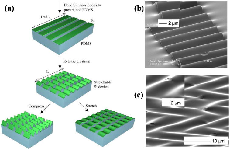
(a) Schematic illustration of the process for fabricating buckled wavy single-crystal silicon ribbons on a PDMS substrate. SEM images of (b) stretchable nanoribbons and (c) stretchable nanomembranes. (Reprinted with permission from [13].)
| (1) |
where hf, Ēf, and Ēs are the thickness, plane-strain Young's modulus of the ribbon, and plane-strain Young's modulus of the substrate, respectively; εpre is the prestrain of the substrate; and εapplied is the applied strain after the wavy structure is formed. More importantly, their analysis shows that the ribbons buckle such that the membrane strain remains a constant εmembrane = −εc and is negligible compared with the bending strain (maximum curvature × hf/2). As a result, the maximum strain in the ribbon (also called peak strain εpeak, which equals the sum of membrane and bending strain) can be written as [18]
| (2) |
This peak strain is much smaller than the prestrain εpre such that the system can provide large stretchability/compressibility. For example, εpeak is only 1.8% for the silicon-on-PDMS system in Fig. 1(b) when εpre = 23.8% and εapplied = 0%.
Jiang et al. [28] and Song et al. [29] pointed out that large-strain finite deformation in the compliant substrate should be considered when the prestrain exceeds 25%; their analyses yield a more accurate description of the system as
| (3) |
and
| (4) |
where λ is from (1) and ξ = 5(εpre – εapplied)(1 + εpre)/32.
These analyses agree well with the experiments and finite element analysis (FEA) results, as shown in Fig. 2(a) for 0% applied strain, and Fig. 2(b) for 16.3% prestrain. When a buckled wavy structure is stretched, it is flatten out when εapplied reaches εpre. At this point, further stretching is applied directly on the nanoribbons; as expected, the structure can be stretched by as much as εstretchability = εpre + εfracture (which we refer to as stretchability). On the other hand, the maximum possible applied compressive strain (or compressibility) is reached when the peak strain εpeak in (4) reaches εfracture and it is well approximated by
Fig. 2.
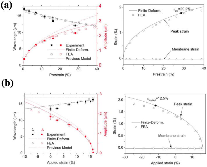
(a) Wavelength, amplitude, membrane, and peak strains of buckled silicon ribbons (100-nm thick) on PDMS as a function of the prestrain. (b) Wavelength, amplitude, membrane, and peak strains of buckled silicon ribbons with prestrain of 16.2% as a function of the applied strain. (Reprinted with permission from [20].)
For silicon with εfracture = 1.8%, the compressibility is about 12.5% for prestrain of 16.3%. Fig. 3 shows the stretchability and compressibility versus various prestrains. The stretchability increases with the prestrain but the compressibility decreases. The Si/PDMS system has equal stretchability and compressibility when the prestrain is 13.4%.
Fig. 3.
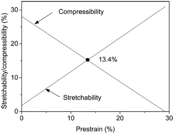
Analytically predicted stretchability and compressibility of buckled silicon ribbons (100-nm thick) on PDMS. (Reprinted with permission from [20].)
To better control the buckle geometries (especially, the wavelength) of silicon or GaAs nanoribbons and to improve the stretchability, more sophisticated surface engineering approaches were developed in [30] via a combined lithographically patterned surface bonding chemistry and similar buckling processes. The fabrication procedure is shown in Fig. 4(a)–(c). Fig. 4(a) shows the photolithography process that defines the bonding chemistry on a PDMS substrate with prestrain of εpre = ΔL/L. The patterning process creates selected regions with activated sites where chemical bonding occurs between the ribbons (GaAs or Si) and the PDMS substrate, as well as inactivated sites where there are only weak van der Waals interactions. Let Wact and Win denote the widths of activated and inactivated sites, respectively [Fig. 4(a)]. Thin ribbons parallel to the prestrain direction are then attached to the prestrained and patterned PDMS substrate [Fig. 4(b)], followed by the relaxation of the prestrained PDMS that leads to buckling of these ribbons due to the physical separation of the ribbons from the inactivated sites on the PDMS [Fig. 4(c)]. The geometrical constraints define the wavelength of the buckled structures as
Fig. 4.
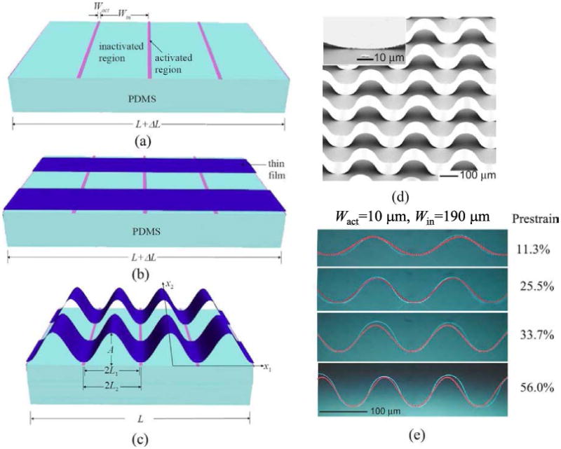
(a) Prestrained PDMS with periodic activated and inactivated patterns. (b) Thin film parallel to the prestrain direction is attached to the prestrained and patterned PDMS substrates. (c) Relaxation of the prestrain in the PDMS leads to buckles of the nanoribbons. (d) SEM image of buckled GaAs nanoribbons formed using (a)–(c). Inset: GaAs/PDMS substrate interface. (e) Buckled GaAs thin films on patterned PDMS substrate for different prestrain levels: 11.3%, 25.5%, 33.7%, and 56.0% (from top to bottom). The red lines are the profiles of the buckled GaAs thin film predicted by the analytical solution. (Reprinted with permission from [22].)
| (5) |
and the amplitude A depends on the geometries of the interfacial patterns (Wact and Win) and the prestrain. Fig. 4(d) shows a tilted-view scanning electron microscope (SEM) image of buckled GaAs ribbons on PDMS, in which εpre = 60%, Wact = 10 μm, and Win = 400 μm.
Jiang et al. [31] developed an analytical model to study the buckling behavior of such systems, and predicted the buckling amplitude and maximum strain in the ribbons as
| (6) |
and
| (7) |
respectively. Fig. 4(e) shows the predicted profiles (red lines) of buckled Gas ribbons given by (5) and (6) for Wact = 10 μm and Win = 190 μm at various prestrain levels, as well as experimental images. Both wavelength and amplitude agree well with experiments. Equation (7) shows that the peak strain is much smaller than the prestrain. For example, εpeak is only 0.6% for hf = 0.3 μm, Wact = 10 μm, Win = 400 μm, and εpre = 60%. Therefore, the precisely controlled buckling can significantly reduce the maximum strain in thin ribbon and improve the system stretchability.
Related discussions on this type of stiff-film-on-elastomer electronic systems regarding the effects of finite ribbon width, global versus local buckling, and similar strategies to achieve stretchable 2-D wrinkled nanomembrane are reported in [32] and [33]. These mechanics analyses provide guidelines in designing electronic systems that use this construction. It is shown in both modeling and experiments that these systems can be stretched by as much as ∼30%, and are compatible with well-developed wafer-based technologies. They enable a wide range of promising applications that require large areal coverage of active components, such as the ones demonstrated in [34] via high-performance, stretchable, and foldable integrated circuits with examples in silicon complementary logic gates, ring oscillators, and different amplifiers.
B. Island-Interconnect Design
1) Island-Interconnect Circuit Mesh on Flat Elastomers
Devices based on wavy inorganic nanoribbons and membranes have limited stretchability because the fracture strengths of inorganic semiconductors are small. To overcome this limitation, Kim et al. [35] developed a strategy where an entire ultrathin circuit system (Fig. 5) is fabricated first and then integrated onto a prestrained elastomer to form wavy interconnected device array. Ko et al. [1] and Kim et al. [36] combined the advantages of selectively bonded wavy structures [Fig. 4(d)] and interconnected circuit arrays to develop a noncoplanar mesh design that significantly improved the stretchability. Fig. 6 schematically shows the fabrication of this type of circuit, which consists of spatially isolated device islands (blue squares in Fig. 6) interconnected by metal interconnects (green strips in Fig. 6) [37]. The island–interconnect mesh design is first obtained on a wafer through photolithographic patterning and etching. The mesh design is then lifted off the wafer onto a slab of PDMS to allow deposition of a thin layer of Cr/SiO2 at the locations of inorganic islands. Transferring the mesh design to a biaxially stretched PDMS substrate after exposing its surface to ozone forms strong chemical bonds at the locations of the islands [similar to the activated area in Fig. 4(a)] and weak bonds at the locations of interconnects [similar to the inactivated area in Fig. 4(a)]. Once the prestrain is released, the interconnects buckled and moved out of the plane to accommodate the deformations such that the strain in the islands remain small.
Fig. 5.
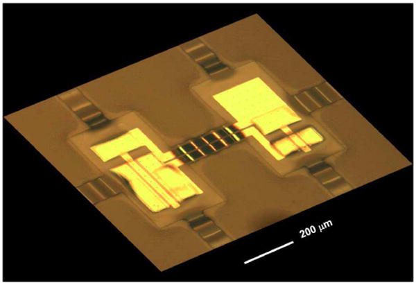
Optical image of CMOS inverters with coplanar mesh design. (Reprinted with permission from [26].)
Fig. 6.
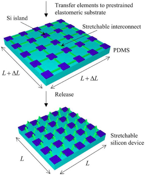
Schematic illustration of the process for fabricating electronics with the island–interconnect mesh designs on a elastomeric substrate. (Reprinted with permission from [28].)
Song et al. [37] established a mechanics model to understand the underlying physics and to guide the design of such systems. Let Eisland, νisland, hisland, Einterconnect, hinterconnect, and denote Young's modulus, Poisson's ratio, the thickness of the islands, Young's modulus, thickness, and the original lengths of the interconnects, respectively. Mechanics analyses reveal that the maximum strain in the interconnects and in the islands are
| (8) |
| (9) |
The maximum allowable prestrain that the island-interconnect mesh design can accommodate is obtained by either or , and can be written as
| (10) |
where
For a ≥ 1 (long interconnects), the maximum prestrain is then governed by the failure of PDMS substrate.
After the prestrain is relaxed, it is interesting to study how much the system can be stretched/compressed before either the interconnect or island fails. The stretchability, which characterizes how much the island–interconnect mesh design can accommodate stretching, is determined by the condition at which the buckled interconnects being stretched to a flat state (i.e., the top frame of Fig. 6). Song et al. [29] performed the analysis and analytically gave the stretchability/compressibility of the island–interconnect design (11), as shown at the bottom of the next page.
Fig. 7 shows the stretchability and compressibility given in (11) versus the prestrain for , hisland = 50 nm, , and hinterconnect = 50 nm. For simplicity, we assume . As the prestrain increases, the stretchability improves but the compressibility worsens. Therefore, prestrain cannot be used to achieve both maximum stretchability and maximum compressibility. Fig. 8 shows the stretchability and compressibility versus the interconnect length for the same set of properties as Fig. 7 and εpre = 50%. As the length of the interconnect increases, both stretchability and compressibility improve. Therefore, the increase in interconnect length (or island spacing) gives both large stretchability and compressibility.
Fig. 7.
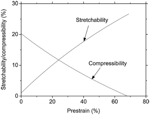
Predicted stretchability and compressibility versus the prestrain for the island–interconnect mesh design (island: 20 × 20 μm2 and 50-nm thick, and interconnect: 20 × 4 μm2 and 50-nm thick) when the failure strains of interconnect and island are 1%. (Reprinted with permission from [28].)
Fig. 8.
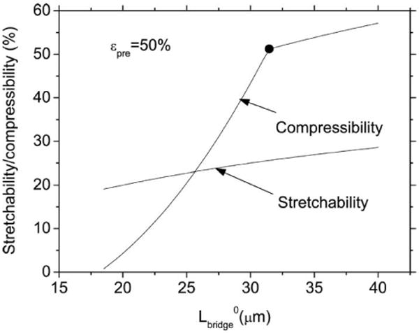
Predicted stretchability and compressibility versus the length of interconnect for the when the prestrain is 50%. The dot on the curve for compressibility separates the failure of interconnect or island (left of the dot) from the contact of neighbor islands (right of the dot). (Reprinted with permission from [28].)
| (11) |
2) Island–Interconnect Circuit Mesh on Curvilinear Elastomers
From the results in Figs. 7 and 8, it is clear that the prestrain can go as high as 60%, and the stretchability is improved to as high as ∼50% for long interconnects. Ko et al. [38] made great use of these features and proposed electronic systems that feature complex curvilinear shapes. Fig. 9 schematically shows the fabrication processes for using island–interconnect circuit mesh layouts and elastomeric transfer elements to wrap electronics onto substrates with complex curvilinear shapes, such as the dimpled surface of the golf ball shown here (top left). The process begins with the fabrication of a thin transfer element in an elastomer such as PDMS by double casting and thermal curing against the object to be wrapped (i.e., the target substrate) (top middle). Radially stretching the resulting element from its rim forms a flat drumhead membrane in which all points in the PDMS are in tension with the levels of strain (from almost 0% at the center of the transfer element to up to ∼60% near the rim) that vary with position. Contacting this stretched transfer element against a prefabricated circuit in a planar ultrathin mesh geometry on a silicon wafer and then peeling it back lifts the circuit onto the PDMS (top right). Relaxing the tension geometrically transforms the membrane and the circuit on its surface into the shape of the target substrate (bottom middle). During this process, the interconnection interconnects of the mesh adopt noncoplanar arc shapes (bottom middle inset), thereby accommodating the compressive forces in a way that avoids significant strains in the islands. Transfer to the corresponding region of the target substrate and removal of the rim completes the process (bottom left). Due to the varied prestrain levels before transferring the circuits, buckling of interconnects on a complex shape, such as a pyramid in Fig. 10(a), often results in different patterns; each interconnect along the circumferential direction buckles to a single arch (i.e., global buckling), but each interconnect along the meridional direction buckles to multiple small arches, which is referred to as local buckling [Fig. 10(c)] here. The interconnects around the top of a parabola [Fig. 10(b) and (d)] do not buckle at all, i.e., no buckling. Wang et al. [39] developed a complete mechanics model to analytically predict the prestrain levels |εpre| (see the detailed analytical expressions in [30]) at different locations on transfer elements of arbitrarily shapes, the different buckling modes, and the resulting different strains in the islands/interconnects mapped at different locations. We showed that the different buckling modes are not only related to the different levels of |εpre|, but also to the various works of adhesion γ between the interconnects and the transfer element, and gave them analytically as
Fig. 9.
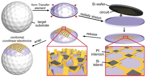
Schematic illustration of the steps for using silicon membrane circuits in mesh layouts (i.e., arrays of islands interconnected by narrow strips) and elastomeric transfer elements to wrap electronics onto substrates with complex curvilinear shapes, such as the dimpled surface of the golf ball shown here. (Reprinted with permission from [29].)
Fig. 10.
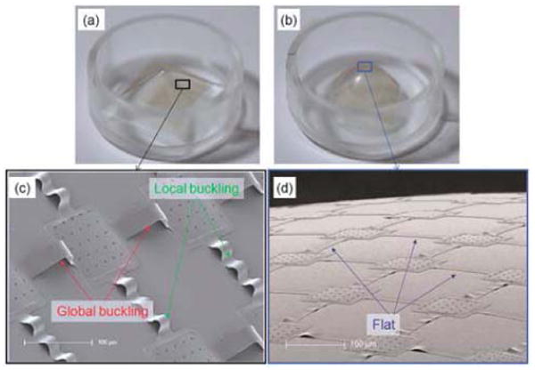
Experimentally observed different buckling patterns of interconnects in different areas of various shapes of curvilinear surfaces. (a) pyramid shape; (b) parabola shape; (c) local and global buckling; (d) no buckling (flat). (Reprinted with permission from [30].)
| (12) |
and
| (13) |
where εc = π2h2/(3L2), and E, h, and L are Young's modulus, the thickness, and the length of the interconnect, respectively. Once the buckling modes are determined, the maximum strains in the interconnects and the islands can be obtained analytically, using similar models in the beginning of this section, as
| (14) |
FEA and experiments were used to verify (12)–(14) and they agreed well for various shapes such as parabola, pyramid, hemisphere, cone, and golf ball [29]. These concepts and analyses provide design guidelines and criteria for many applications that adopt curvilinear shapes, especially for important bioinspired designs (e.g., hemispherical electronic eye camera [1]) and biointegrated designs (e.g., cardiac mapping devices [38], [40]) that features shapes similar/identical to human body parts.
3) Island–Interconnect Circuit Mesh on Trenched Elastomers
It is clearly shown in Fig. 8 that the island–interconnect design demands long interconnects to achieve high stretchability, but long interconnects also mean that the spacing between the islands (active devices) are large. This limits its application on some of the systems that require high areal coverage, such as photodetection and photovoltaics, where such layouts are important. Lee et al. [41] proposed an advanced approach that builds on ideas similar to the island–interconnect structure, but in configurations where the devices mount on raised islands and the interconnects between them buckle downward into separating trenches. A representative layout for a structured substrate designed for this purpose appears in Fig. 11, in which the relief consists of isolated raised regions (i.e., islands) separated by recessed features (i.e., trenches). The casting and curing processes of soft lithography [42] provide a convenient means to form such relief, with an excellent dimensional control, in elastomers such as PDMS. Fig. 11(a) provides a cross-sectional view for a representative case where square islands with edge lengths (lisland) of 800 μm are separated by trenches with widths (ltrench) and depths (htrench) of 156 and 200 μm, respectively. The thickness of the underlying PDMS (i.e., base) is 200 μm. This type of structure is attractive for stretchable systems that incorporate nonstretchable active elements at the islands because it isolates strains from these regions. In particular, for this example, stretching the substrate [Fig. 11(a)] to an overall strain of ∼20% induces elongations (∼123%) in the trenches that are much higher (>300 times) than those at the islands (∼0.4%). The FEA quantitatively captures this basic mechanics. In particular, for 20% overall strain, FEA yields a 124% increase in ltrench (i.e., 156–349 μm), which is very close to the value (∼123%) obtained from experiment. FEA gives a very small change (0.3%) in lisland, similar to that (∼0.4%) from experiments. These results show that the large deformation of the system is highly isolated in the trench and does not deform the island much, which is a great feature that protects the active inorganic components on the islands from fracture.
Fig. 11.
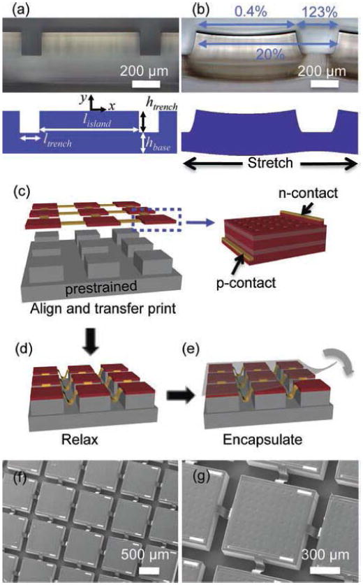
Optical microscopy images and FEA calculations of deformation of a slab of PDMS and schematic illustrations of the steps in the fabrication of stretchable GaAs photovoltaic modules with SEM images of a completed device. Cross-sectional optical microscopy images (top) and FEA (bottom) of a slab of PDMS in (a) relaxed and (b) stretched states, with a square array of raised islands (each ∼800 μm × 800 μm) separated by recessed trenches (widths ∼156 μm and depths ∼200 μm), designed as a platform for (c) stretchable inorganic photovoltaics with high areal coverages. (d) Releasing the prestrain and pressing on the entire array using a flat plate of glass deform the interconnects into arc-shaped interconnects, in a vertical downward orientation, into the trench regions of the PDMS substrate as illustrated here. (e) In a final step, a thin (∼50 μm), uniform layer of PDMS is bonded on the top, as an encapsulant to protect the system from the environment. (f) and (g) SEM images of a completed module. (Reprinted with permission from [34].)
The strains in the interconnects (εinterconnect) and device islands (island) εisland for the as-fabricated state can be given analytically in terms of the prestrain εpre as
| (15) |
and
| (16) |
where yinterconnect and yisland are the distance to the neutral axis of the interconnect and island, respectively; and (EI)interconnect and (EI)island are the bending stiffness of the interconnect and the island, respectively. These equations give an analytical method to design the geometry of the trenches, islands, and thicknesses of devices. Lee et al. [43] proposed a similar but more elaborate scheme that uses notched islands and trenches to further increase the degree of stretchability and the areal coverage, as well as to provide a natural form of strain-limiting behavior, and therefore help avoid destructive effects of extreme deformations. They also demonstrated its application in high-efficiency dual-junction GaInP/GaAs photovoltaics.
C. Curved Interconnect Designs and Ultrasoft Electronics
The designs in Sections II-A and II-B all adopt buckled straight interconnects and therefore cannot be used when prestrain is impossible/difficult; in addition, because these systems can only be stretched as much as the prestrain (when the interconnect are stretched to their flat state), they are not suited for many applications where stretchability of > 50% are required.
1) Serpentine Interconnects
To overcome these limitations and expand the deformability even further, without increasing the sparseness of the distribution of islands, serpentine interconnects can be used [36]. Fig. 12(a) shows the SEM images of such a design after executing the fabrication procedures of Fig. 6. When external strain is applied along the x- or y-direction, these noncoplanar serpentine interconnects effectively compensate the applied strain not only through changes in height (out-of-plane buckling) but also by changes in geometry of the serpentine shape. Fig. 12(b) shows the images of the response of a representative device to on-axis stretching strains up to 70%, for a system built with 35% prestrain, in which deformations of the serpentine interconnects exhibit changes in configurations that might be expected intuitively. Remarkably, FEA reveals that, even to stretching strains of 70%, the peak strains in the metal layer in the interconnects and islands are 0.2% and 0.5%, respectively, and the strain in silicon is 0.15%, as shown in Fig. 12(c).
Fig. 12.
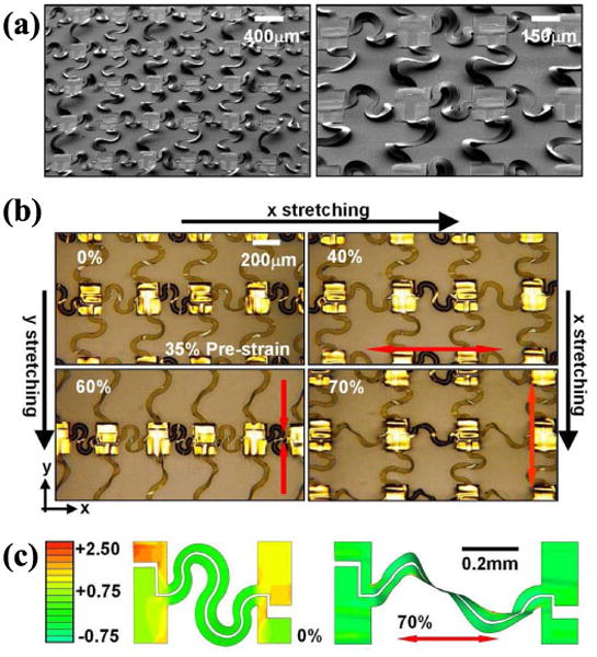
Mechanical and electrical responses of island–interconnect stretchable electronics to in-plane strains. (a) SEM image of an array of stretchable CMOS inverters with noncoplanar bridges that have serpentine layouts (left) and magnified view (right). (b) Optical images of stretching tests in the x- and y-direction. (c) FEM simulation before (35% prestrain) and after (70% applied strain) stretching. (Reprinted with permission from [27].)
Zhang et al. [44] developed a mechanics model to study the onset of buckling and postbuckling behaviors of this type of interconnects, with geometric parameters l1 and l2, width w, thickness t, and the number of unit cells m shown in Fig. 13(a). Upon stretching of the entire structure, the interconnect is pulled from the two ends, such that each straight and arc wire segments undergoes combined shearing and bending. As the applied strain reaches a critical value, lateral buckling (or shear buckling) occurs to reduce the strain energy. Zhang et al. [44] analyzed this critical buckling strain and found that it is linearly proportional to the square of aspect ratio, t2/w2, and is given by
Fig. 13.
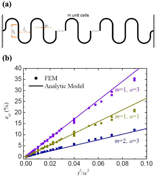
(a) Illustration of geometric parameters for a serpentine interconnect with m unit cells. (b) Critical buckling strain of serpentine interconnect under stretching, obtained from the analytic model and FEA. (Reprinted with permission from [35].)
| (17) |
where α = l2/l1, G and E are the shear and Young's moduli of the interconnect, respectively, and f1, f2, and f3 are the functions that depend only on the number of unit cells m (see [35] for details). FEA results validate this scaling law for a wide range of aspect ratios α and t/w, as shown in Fig. 13(b). As the applied strain exceeds the critical buckling strain given in (17), the serpentine structures undergo lateral buckling to reduce the strain energy, and accordingly, the strain level in the structure. The maximum strain in the interconnect is given analytically as
| (18) |
where g1 and g2 are the nondimensional functions of the number of unit cell m, and α (see [35] for details). Based on (18) and the yield criterion of εmax = εyield, where εyield is the yield strain of the interconnect material, the elastic stretchability of the serpentine can be written as
| (19) |
where λ > 0 is the solution of the following fourth-order algebraic equation that has a single positive solution:
| (20) |
These predictions agree well with the numerical results for a large range of t/w and εyieldl1/w, as shown in Fig. 14(a) and (b). To calculate the ultimate stretchability of the structure, as defined by the applied strain required to induce εmax that reaches the failure strain εfail, (19) and (20) can be used with εyield replaced by εfail. The collective results reviewed here allow straightforward optimization in designs of serpentine structures for large stretchability.
Fig. 14.
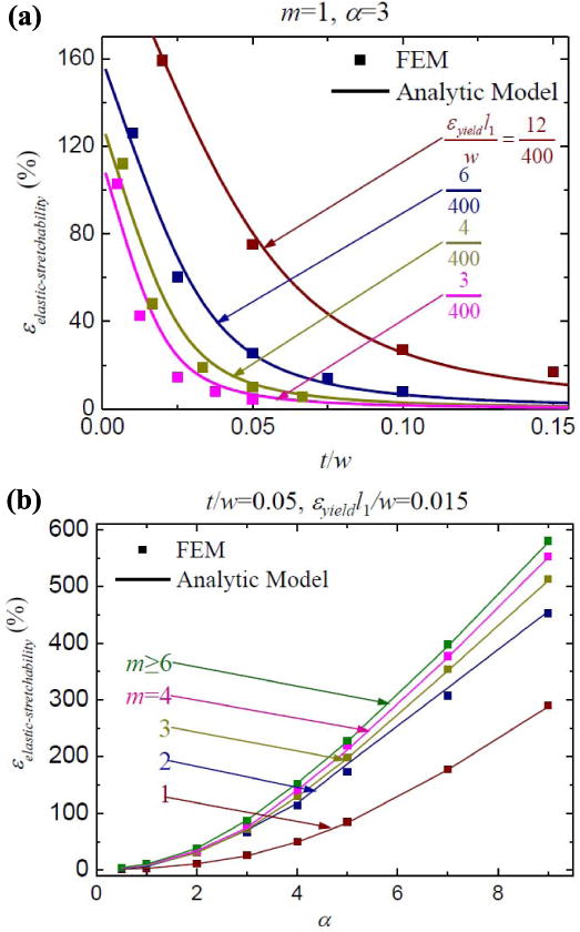
Scaling law of elastic stretchability. (a) Elastic stretchability versus cross section aspect ratio t/w for various εyieldl1/w, m = 1 and α = 3. (b) Elastic stretchability versus the length/spacing ratio α of interconnect for various unit cell number m, t/w = 0.05, εyieldl1/w = 0.015. (Reprinted with permission from [35].)
Kim et al. [40] reported the applications of this category of serpentine interconnects through demonstrations of sensor webs designed for epicardial electrogram mapping [Fig. 15(a) and (b)], strain gauges [Fig. 15(c)], and balloon catheter [Fig. 15(d) and (e)], all of which feature deformations of >50% and serpentine interconnects between the isolated device islands. Xu et al. [7] also reported similar concepts to 3-D, multifunctional cardiac measurements, and stimulation across the entire epicardium [Fig. 15(f) and (g)].
Fig. 15.
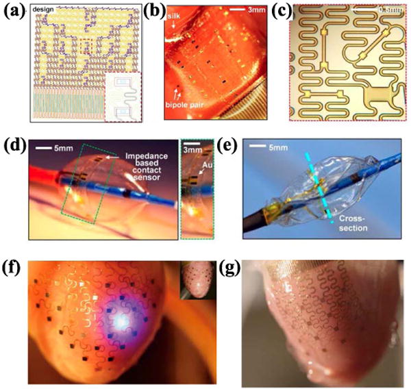
(a) Layout of a sensor Web designed for epicardial electrogram mapping. Inset: magnified views of a pair of electrodes and the serpentine interconnects. (b) Web mounted on the epicardial surface. (c) Strain rosettes with longitudinal, diagonal, and transverse Si nano membrane piezoresistors. (d) and (e) Impedance-based contact sensor webs, on collapsible balloon catheters and deflated state. (f) and (g) 3-D multifunctional integumentary membranes for spatiotemporal measurement and stimulation across the entire epicardial surface. (Reprinted with permission from [7] and [31].)
2) Fractal Interconnects
Fractal-based structures can be described by self-similarity: subdivision into small sections yields pieces with geometries that resemble the whole. Compared with the previously explored networks of periodic serpentine shapes, fractal designs can be engineered to accommodate enhanced elastic strain along a selected dimension and to support biaxial, radial, and other deformation modes. In addition, the choices of topologies span a rich range, from lines to loops, capable of tailoring to specific electronic applications through integration and interdigitation of multiple structures. Fig. 16 shows six representative examples, from lines (Koch, Peano, and Hilbert) to loops (Moore and Vicsek) and branch-like meshes (Greek cross) [45]. The results illustrate the diversity of possibilities through both the FEA and experimental demonstration. The approximate fractal dimensions in these finite-iterative curves range from 1.5 to 2. The elastic tensile strains achieved with these structures indicate that they are suitable for use in various stretchable devices, with the key advantages over previously described layouts. Zhang et al. [46] analyzed the fractal structures of different shapes, any self-similar orders and gave analytically the maximum strain εmax in the structure under stretching (see [37] for details). By setting εmax equal to the yield strain of the materials, stretchability of the structure can be obtained. Fig. 17 shows the normalized stretchability versus the order n for self-similar rectangular and serpentine interconnects, from both analytic analysis and FEA. The stretchability is more than doubled for each n increasing by 1, indicating the elastic limit of the interconnect can be well improved by adopting higher order self-similar design. Zhang et al. [47] also proposed a hierarchical computational model for postbuckling analysis of fractal interconnects based on the mechanism of ordered unraveling. The approach substantially reduces the computational efforts and costs compared with conventional FEA, but with accurate predictions. These analytic and computational models are useful for the development of stretchable electronics that simultaneously demand large areal coverage of active devices. Design optimization shows that the higher order self-similar interconnect gives stretchability of 70%–90% for different surface filling ratio of active devices.
Fig. 16.
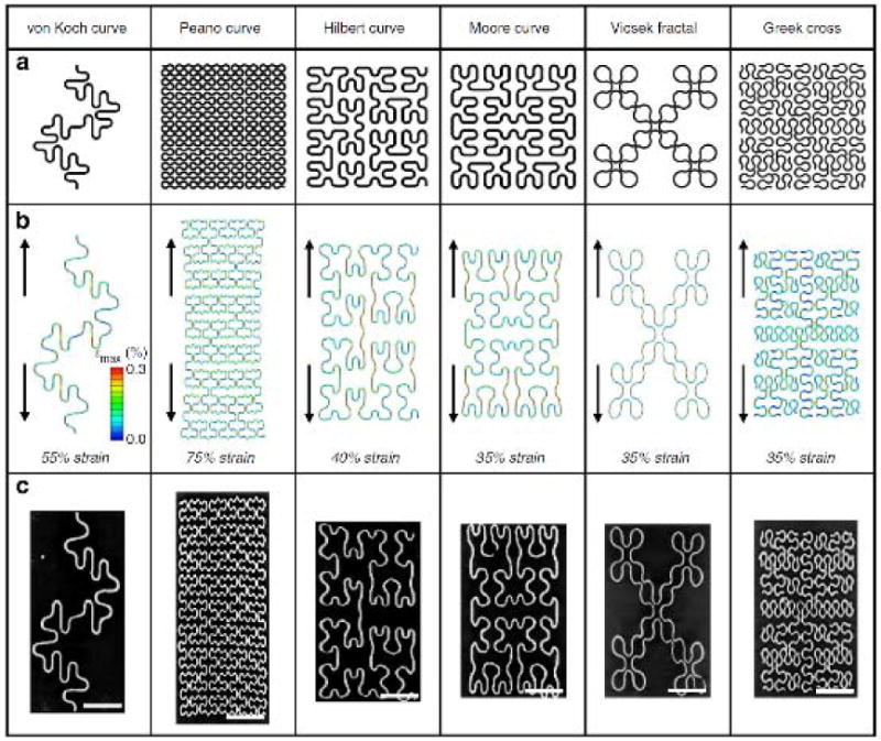
Representative fractal-inspired layouts for hard–soft materials integration. (a) Six different patterns of metal wires fully bonded to elastomer substrates demonstrate the application of deterministic fractal designs as general layouts for stretchable electronics. (b) FEM images of each structure under elastic tensile strain. (c) Their corresponding experimental micro-XCT (X-ray Computed Tomography) images demonstrate the elastic mechanics. (Reprinted with permission from [36].)
Fig. 17.
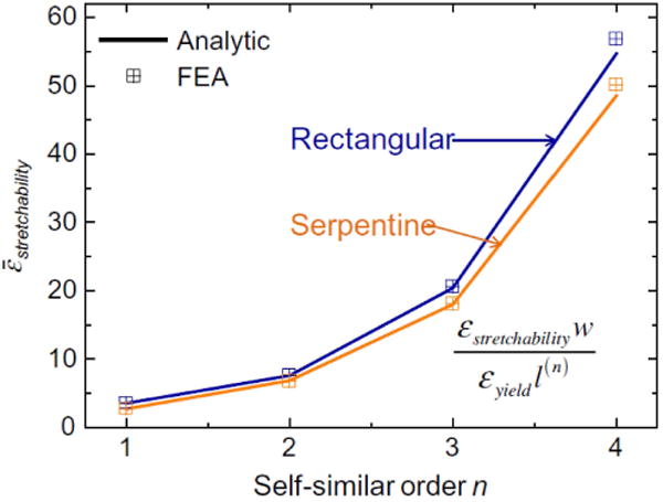
Normalized stretchability as a function of the self-similar order. (Reprinted with permission from [37].)
3) Ultrasoft Biointegrated Electronics
In addition to large stretchability, curved interconnects also lower the overall system stiffness and, therefore, are attractive options for electronic systems that are ultrasoft, tissue-like, and biocompatible.
A representative work that provides mechanical insights into this was reported in [48], in which the elasticity of an order-n fractal-inspired interconnects of arbitrary shape are determined analytically and verified experimentally. The analysis starts with a fractal shape given in the Cartesian coordinates Y = Y(X) (Fig. 18). At each fractal order, the interconnect has the same centro-symmetric shape, but the total arc length increases by a factor η as the fractal order increases by 1. Define
Fig. 18.
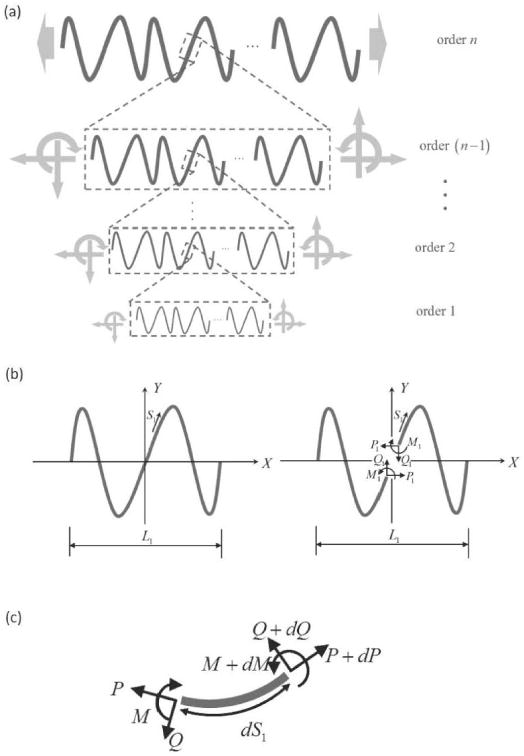
(a) Schematic illustrations of the fractal interconnects with any centro-symmetric shape in a representative element. (b) Curvilinear coordinate S1 along the arc length direction and the internal forces. (c) Sign convention for the internal axial force P, shear force Q, and bending moment M. (Reprinted with permission from [39].)
| (21) |
where β1 is the ratio of total length to apparent length, and all other shape parameters β2–β6 depend only on β1 for a given fractal shape. Energy analysis and force equilibrium yield expressions for dimensionless coefficients as
| (22) |
For an order-n fractal interconnect between two active device islands with the spacing L, the tensile stiffness for a representative element of apparent length L is given by
| (23) |
where is the bending stiffness of the order-1 interconnect. Fig. 19 shows the experimental and analytical results of force–displacement curves for zigzag [Fig. 19(a)], sinusoidal [Fig. 19(b)], and serpentine [Fig. 19(c)] fractal structures. The results given from (23) agree well with experiments.
Fig. 19.
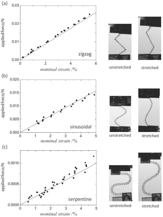
Comparison between the experimental and analytic force-nominal strain curves and the optical microscope images for undeformed and deformed interconnects for (a) zigzag, (b) sinusoidal, and (c) serpentine fractal shapes with fractal order n = 2. (Reprinted with permission from [39].)
For the zigzag shape, Fig. 20 shows the normalized tensile stiffness versus β1 with the fractal order-n ranging from 1 to 4. It is clear that the fractal interconnect becomes more compliant as the fractal order n or the total length (represented by β1) increases. The tensile stiffness is validated by the FEA. The numerical results shown in Fig. 20 for the size ratio n = 10 across each order agree well with (23). The normalized tensile stiffness for the zigzag, sinusoidal, and serpentine fractal shapes and the fractal order n = 2 in Fig. 21 suggests that, for the same ratio of total length to apparent length β1, the dependence on these three shapes is relatively weak.
Fig. 20.
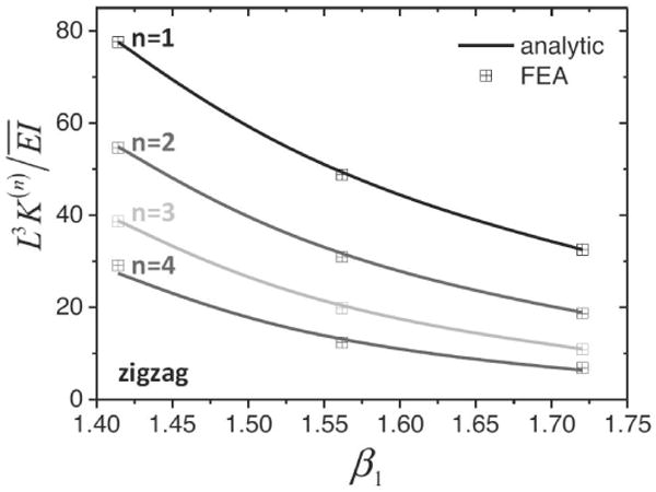
Normalized tensile stiffness versus the ratio of the total length to apparent length β1 for the zigzag fractal shape with the fractal order n ranging from 1 to 4. (Reprinted with permission from [39].)
Fig. 21.
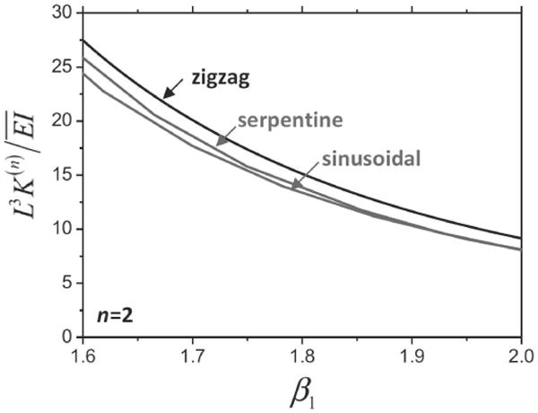
Normalized tensile stiffness for the zigzag, sinusoidal, and serpentine fractal shapes and the fractal order n = 2. (Reprinted with permission from [39].)
With the mechanics analysis, it is possible to make use of analytical expressions, e.g., (23) here, to select materials and geometries of the interconnecting interconnects, such that the overall system stiffness is as low as desired. Ultrasoft and stretchable electronic systems such as stretchable batteries [9] and fractal designs for epidermal electronics [45], [49] become possible. More importantly, when the stiffness of the electronic system is comparable or even smaller than the biological tissues, it is possible to mount these devices onto the surfaces of tissues for health monitoring and therapeutic applications. Kim et al. [3] combined the advantages of the serpentine design (islands were reduced to sizes matched to the widths of the interconnects) and ultrathin geometries and proposed a class of electronics that has mechanical properties matched to that of the epidermis, which we refer to as epidermal electronic systems (EES) here. By carefully tuning the geometries and mechanics of the island–interconnect design, the overall stiffness of the EES is lower than that of the skin, as shown in Fig. 22(a). The resulting EES can be directly transferred and mounted onto the skin without applications of any adhesive or mechanical clamps, much like the fashion of a temporary tattoo [Fig. 22(b) and (c)]. Intimate reliable contact between the EES and the epidermis is achieved naturally by van der Waals interactions only, and enables the applications that provide comfortable and portable health-monitoring attachments or human–machine interfaces [3].
Fig. 22.
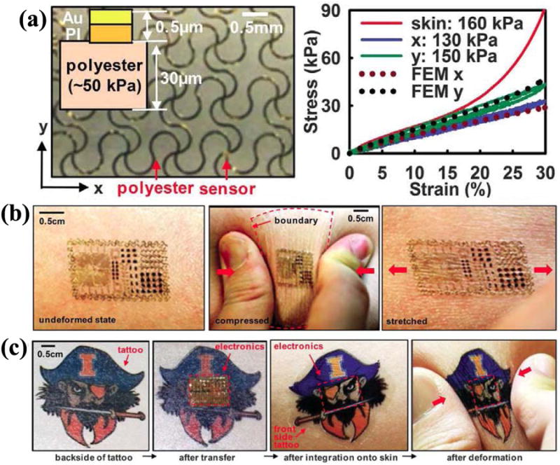
(a) Left: optical micrograph of an EES with filamentary serpentine design. Right: stress–strain data from uniaxial tensile measurements for two orthogonal directions. Data collected from a sample of pig skin are also presented. The dotted lines correspond to calculation performed with FEA. (b) Multifunctional EES on skin: undeformed (left), compressed (middle), and stretched (right). (c) Commercial temporary transfer tattoo provides an alternative to polyester/polyvinyl-alcohol for the substrate; in this case, the system includes an adhesive to improve bonding to the skin. Images are of the backside of a tattoo (far left), electronics integrated onto this surface (middle left), and attached to skin with electronics facing down in undeformed (middle right) and compressed (far right) states. (Reprinted with permission from [3].)
D. Prestrain Strategy for Ultrastretchable Electronics
The advantage of prestrained straight interconnects and that of the curved interconnect designs can be combined to develop electronic systems that are ultrastretchable. Zhang et al. [50] proposed a prestrain serpentine interconnect design, which is shown in Fig. 23(a). Serpentine interconnects are transfer printed and bonded onto a stretched substrate; releasing the strain causes deformations in the interconnect that configure it into a form with enhanced stretchability. SEM images in Fig. 23(b) and (c) show serpentine interconnects before and after release of the prestrain (εpre = 160%) of a soft elastomeric substrate (Ecoflex, Smooth-On, Inc).
Fig. 23.
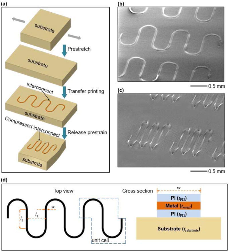
(a) Schematic illustration of the prestrain strategy for fabricating serpentine interconnects with enhanced levels of stretchability. (b) SEM image of the serpentine structures before releasing the prestrain of the substrate. (c) SEM image of the serpentine interconnect after releasing the prestrain of the substrate. (d) Illustration of the geometric parameters for a serpentine interconnect, with top and cross-sectional views. (Reprinted with permission from [41].)
For a serpentine interconnect bonded to a soft substrate and subject to stretching εappl along the horizontal direction [Fig. 23(a)], the straight segment in the vertical direction in the serpentine interconnect undergoes compression due to the Poisson effect, and therefore buckles/wrinkles into wavy shapes. An analytical model was developed to study the buckling behavior of this prestrained serpentine interconnects, and the buckling wavelength is given by
| (24) |
where Ēsub is the plane-strain Young's modulus of the elastomeric substrate, and Sinterconnect is the effective bending stiffness of the interconnect that depends on Young's moduli and the thicknesses of the top three layers shown in Fig. 23(d) (right frame). When the wavelength given in (24) is smaller than the straight segment of the serpentine [l2 in Fig. 23(d), left], i.e., λ < l2, local wrinkling occurs; otherwise, the interconnect deforms without wrinkling. For a copper serpentine interconnect fully attached to an Ecoflex substrate, with the thickness of each polyimide layer tPI = 1.2 μm, Fig. 24(a) shows that the above analytic criterion gives the critical thickness of metal layer separating the two buckling modes as 0.9 μm, which is slightly underestimated as compared with the experiments and FEA. Fig. 24(b) and (c) shows the 3-D configurations of the deformed serpentine interconnect from FEA and experiments (based on 3-D micro-XCT scanning), respectively. Local wrinkling is clearly observed for thin metal layers (0.3 and 0.6 μm), and no wrinkling for relatively large metal layers (1.6 μm). The wavelengths given by FEA and experiments also agree very well.
Fig. 24.
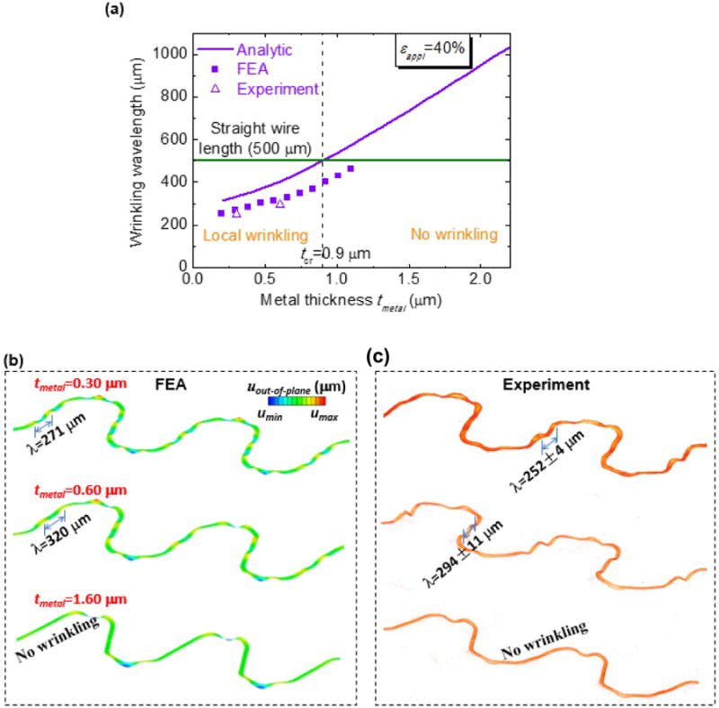
(a) Dependence of wrinkling wavelength on the metal thickness, based on the experiments, numerical simulations, and analytic modeling. (b) Numerical results and (c) 3-D XCT scanning images of the deformed configurations for three typical metal thicknesses to illustrate the different buckling modes. (Reprinted with permission from [41].)
The ultimate (one-time tensile load) and elastic (cyclic load) stretchability of the prestrained interconnect was also studied by both FEA and experiments for different prestrain levels. Fig. 25(a) shows the deformations after relaxation of different levels of prestrain from both experiment and FEA. For the sample with a prestrain level of 85% that avoids plastic deformation in the compressed serpentine interconnect, onetime stretching experiments give the ultimate stretchability as (283 ± 11.5)% [Fig. 25(b) and (c)], which agrees well with 307% from FEA. This is more than two times larger than 120% for the serpentine sample without prestrain (or εpre = 0%). More importantly, cyclic testing and FEA both show that the sample with 85% prestrain can sustain cyclic loading of the magnitude of ∼185% for about 25000 cycles (low cycle test, Fig. 26), while the one without prestrain can only sustain a much lower cyclic load magnitude of 53%.
Fig. 25.
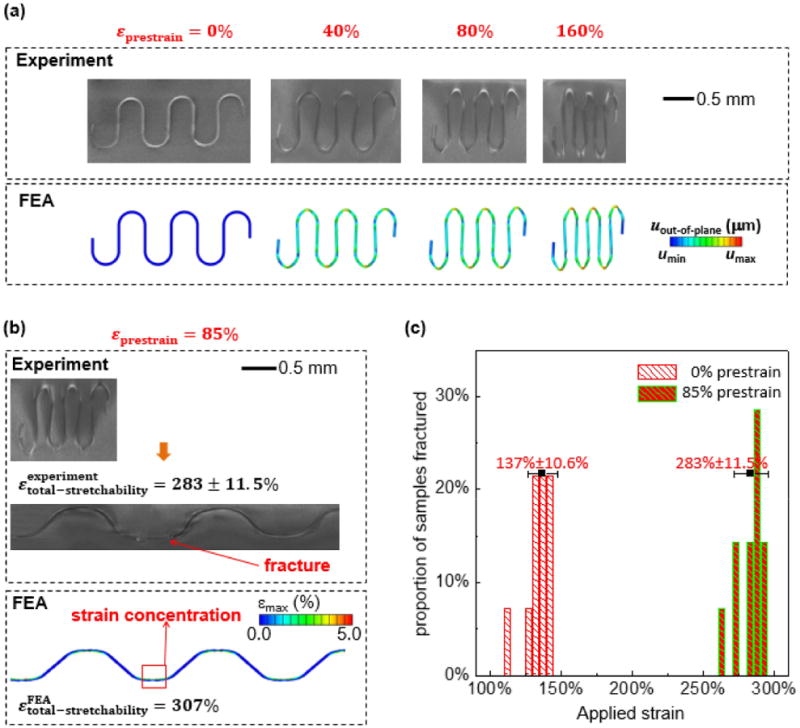
(a) Experimental and numerical analyses of configurations of serpentine interconnects after relaxing different levels of prestrain. (b) Experimental image of the serpentine interconnect and the fracture sites due to one-time stretching (300%), and FEA results for the strain distribution when stretched to the predicted total stretchability (307%), for the case of 85% prestrain. (c) Histogram showing proportions of fractured interconnects at different intervals of applied strain for nonprestrained samples and 85% prestrained samples. (Reprinted with permission from [41].)
Fig. 26.
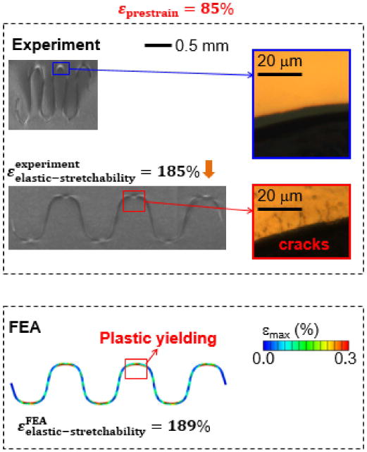
Experimental image of the serpentine interconnect and the fracture sites due to cyclic stretching (with an amplitude of 185% for 25 000 cycles), and fea results for the strain distribution when stretched to the predicted elastic stretchability (189%), for the case of 85% prestrain. (Reprinted with permission from [41].)
The prestrain strategy with bonded serpentine interconnect designs yields significantly improved mechanics, in terms of the range of stretchability and maximum strains for different levels of ultimate tensile and cyclic loadings. Both the experimental measurement and numerical simulations verify increases in the elastic and total stretchability to more than two times over samples without prestrain. The prestrain process and its combination with other strategies presented in this paper such as the fractal, strain-isolating, and island–interconnect designs, provide great options for future work in stretchable inorganic device systems.
III. Conclusion
This paper reviews the designs of inorganic circuits for different levels of stretchability: 1) buckled nanoribbons and nanomembranes on elastomer; 2) buckled island–interconnect mesh on flat or curved elastomers, with options of selective bonding and strain-isolating designs; 3) curved interconnect in serpentine fractal shapes; and 4) prestrain strategy for enhanced stretchability. Through discussions of the underlying mechanics and materials theories, fabrication processes for microscale/nanoscale devices, and experimental characterization, optimization criteria are highlighted for future development of this class of electronics. Advantages and disadvantages, as well as the stretchability levels of each design are discussed for selection and combined use of different designs to meet different requirements for a wide range of biocompatible applications. Mechanics theories and modeling play a key role in understanding the physics and design considerations, as well as developing new concepts and ideas that stimulate the further development of stretchable inorganic electronics. The alignment of key aspects of these strategies with entrenched capabilities in materials, manufacturing, circuit design, and packaging strategies for conventional electronics represents a key advantage that can accelerate translation from exploratory research to products. Work in this direction holds promise for the realization of new and important classes of consumer, industrial, and medical devices that lie outside of the scope of existing technologies.
Acknowledgments
The work of S. Wang was supported by the National Science Foundation of China (NSFC) under Grant 11272260, Grant 11172022, Grant 51075327, and Grant 11302038. The work of y. Huang was supported in part by the Division of Civil, Mechanical and Manufacturing Innovation within NSF under Grant cmmi-1400169 through the Division of Materials Research under Grant 1121262, and in part by the National Institutes of Health under Grant r01eb019337. The work of J. A. Rogers was supported in part by the U.S. Department of Energy, Washington, DC, USA, in part by the Office of Science, and in part by the Basic Energy Sciences, under Award de-fg02-07er46741. Recommended for publication by Associate Editor H. Jiang upon evaluation of reviewers' comments.
Biographies

Shuodao Wang received the B.S. degree in engineering mechanics from Tsinghua University, Beijing, China, in 2007, and the Ph.D. degree in mechanical engineering from Northwestern University, Evanston, IL, USA, in 2012.
He was a Post-doctoral Research Associate with the Department of Materials Science and Engineering, University of Illinois at Urbana-Champaign, Urbana, IL, USA, from 2012 to 2014. In 2014, he joined the School of Mechanical and Aerospace Engineering, Oklahoma State University, Stillwater, OK, USA, as an Assistant Professor.

Yonggang Huang received the B.S. degree in mechanics from Peking University, Beijing, China, in 1984, and the M.Sc. and Ph.D. degrees in engineering science from Harvard University, Cambridge, MA, USA, in 1987 and 1990, respectively.
He is currently the Joseph Cumming Professor of Mechanical Engineering and Civil and Environmental Engineering with Northwestern University, Evanston, IL, USA.
Dr. Huang's most recent awards include the Richards Award in 2010 and Drucker Medal in 2013 from the American Society of Mechanical Engineers and ISI Highly Cited Researcher in Materials Science in 2014. He is the Editor of the Journal of Applied Mechanics (Transactions of the ASME).

John A. Rogers received the B.A. degree in chemistry and B.S. degree in physics from The University of Texas at Austin, Austin, TX, USA, in 1989, and the M.S. degrees in physics and chemistry in 1992 and the Ph.D. degree in physical chemistry in 1995 from the Massachusetts Institute of Technology, Cambridge, MA, USA.
He was a Junior Fellow with the Harvard University Society of Fellows, from 1995 to 1997. He joined Bell Laboratories as a member of Technical Staff with the Condensed Matter Physics Research Department in 1997, and served as the Director of Condensed Matter Physics Research Department from 2000 to 2002. He is currently the Swanlund Chair with the University of Illinois at Urbana-Champaign, Urbana, IL, USA, where he is also the Director of the Seitz Materials Research Laboratory.
Contributor Information
Shuodao Wang, Email: shuodao.wang@okstate.edu, School of Mechanical and Aerospace Engineering, Oklahoma State University, Stillwater, OK 74078 USA.
Yonggang Huang, Email: y-huang@northwestern.edu, Department of Civil and Environmental Engineering, and Department of Mechanical Engineering, Northwestern University, Evanston, IL 60208 USA.
John A. Rogers, Email: jrogers@illinois.edu, Frederick Seitz Materials Research Laboratory, Department of Materials Science and Engineering, Department of Electrical and Computer Engineering, and the Department of Chemistry, Beckman Institute for Advanced Science and Technology, University of Illinois at Urbana-Champaign, Champaign, IL 61820 USA.
References
- 1.Ko HC, et al. A hemispherical electronic eye camera based on compressible silicon optoelectronics. Nature. 2008 Aug;454:748–753. doi: 10.1038/nature07113. [DOI] [PubMed] [Google Scholar]
- 2.Jin HC, Abelson JR, Erhardt MK, Nuzzo RG. Soft lithographic fabrication of an image sensor array on a curved substrate. J Vac Sci Technol B. 2004;22(5):2548–2551. [Google Scholar]
- 3.Kim DH, et al. Epidermal electronics. Science. 2011 Aug;333(6044):838–843. doi: 10.1126/science.1206157. [DOI] [PubMed] [Google Scholar]
- 4.Lumelsky VJ, Shur MS, Wagner S. Sensitive skin. IEEE Sensors J. 2001 Jun;1(1):41–51. [Google Scholar]
- 5.Someya T, Sekitani T, Iba S, Kato Y, Kawaguchi H, Sakurai T. A large-area, flexible pressure sensor matrix with organic field-effect transistors for artificial skin applications. Proc Nat Acad Sci USA. 2004 Jul;101(27):9966–9970. doi: 10.1073/pnas.0401918101. [DOI] [PMC free article] [PubMed] [Google Scholar]
- 6.Nathan A, et al. Amorphous silicon detector and thin film transistor technology for large-area imaging of X-rays. Microelectron J. 2000 Dec;31(11–12):883–891. [Google Scholar]
- 7.Xu L, et al. 3D multifunctional integumentary membranes for spatiotemporal cardiac measurements and stimulation across the entire epicardium. Nature Commun. 2014 Feb;5 doi: 10.1038/ncomms4329. Art. id 3329. [DOI] [PMC free article] [PubMed] [Google Scholar]
- 8.Hwang SW, et al. High-performance biodegradable/transient electronics on biodegradable polymers. Adv Mater. 2014;26(23):3905–3911. doi: 10.1002/adma.201306050. [DOI] [PubMed] [Google Scholar]
- 9.Xu S, et al. Stretchable batteries with self-similar serpentine interconnects and integrated wireless recharging systems. Nature Commun. 2013 Feb;4 doi: 10.1038/ncomms2553. Art. id 1543. [DOI] [PubMed] [Google Scholar]
- 10.Brosteaux D, Axisa F, Gonzalez M, Vanfleteren J. Design and fabrication of elastic interconnections for stretchable electronic circuits. IEEE Electron Device Lett. 2007 Jul;28(7):552–554. [Google Scholar]
- 11.Vanfleteren J, et al. Printed circuit board technology inspired stretchable circuits. MRS Bull. 2012;37(3):254–260. [Google Scholar]
- 12.Hsu YY, Gonzalez M, Bossuyt F, Vanfleteren J, De Wolf I. Polyimide-enhanced stretchable interconnects: Design, fabrication, and characterization. IEEE Trans Electron Devices. 2011 Aug;58(8):2680–2688. [Google Scholar]
- 13.Lacour SP, Jones J, Suo Z, Wagner S. Design and performance of thin metal film interconnects for skin-like electronic circuits. IEEE Electron Device Lett. 2004 Apr;25(4):179–181. [Google Scholar]
- 14.Lacour SP, Jones J, Wagner S, Li T, Suo Z. Stretchable interconnects for elastic electronic surfaces. Proc IEEE. 2005 Aug;93(8):1459–1467. [Google Scholar]
- 15.van der Sluis O, Hsu YY, Timmermans PHM, Gonzalez M, Hoefnagels JPM. Stretching-induced interconnect delamination in stretchable electronic circuits. J Phys D, Appl Phys. 2011;44(3):034008. [Google Scholar]
- 16.Lacour SP, Wagner S, Huang Z, Suo Z. Stretchable gold conductors on elastomeric substrates. Appl Phys Lett. 2003;82(15):2404–2406. [Google Scholar]
- 17.Bossuyt F, Günther J, Löher T, Seckel M, Sterken T, de Vries J. Cyclic endurance reliability of stretchable electronic substrates. Microelectron Rel. 2011;51(3):628–635. [Google Scholar]
- 18.Lin KL, Jain K. Design and fabrication of stretchable multilayer self-aligned interconnects for flexible electronics and large-area sensor arrays using excimer laser photoablation. IEEE Electron Device Lett. 2009 Jan;30(1):14–17. [Google Scholar]
- 19.Cotton DPJ, Graz IM, Lacour SP. A multifunctional capacitive sensor for stretchable electronic skins. IEEE Sensors J. 2009 Dec;9(12):2008–2009. [Google Scholar]
- 20.Carta R, et al. Design and implementation of advanced systems in a flexible-stretchable technology for biomedical applications. Sens Actuators A, Phys. 2009;156(1):79–87. [Google Scholar]
- 21.Hu L, et al. Stretchable, porous, and conductive energy textiles. Nano Lett. 2010;10(2):708–714. doi: 10.1021/nl903949m. [DOI] [PubMed] [Google Scholar]
- 22.Song J, Jiang H, Huang Y, Rogers JA. Mechanics of stretchable inorganic electronic materials. J Vac Sci Technol A. 2009;27(5):1107–1125. [Google Scholar]
- 23.Hozumi A, Masuda T, Sugimura H, Kameyama T. Oxide nanoskin formed on poly(methyl methacrylate) Langmuir. 2003 Sep;19(18):7573–7579. [Google Scholar]
- 24.Bowden N, Brittain S, Evans AG, Hutchinson JW, Whitesides GM. Spontaneous formation of ordered structures in thin films of metals supported on an elastomeric polymer. Nature. 1998 May;393:146–149. [Google Scholar]
- 25.Khang DY, Jiang H, Huang Y, Rogers JA. A stretchable form of single-crystal silicon for high-performance electronics on rubber substrates. Science. 2006 Jan;311(5758):208–212. doi: 10.1126/science.1121401. [DOI] [PubMed] [Google Scholar]
- 26.Choi WM, Song J, Khang DY, Jiang H, Huang YY, Rogers JA. Biaxially stretchable ‘wavy’ silicon nanomembranes. Nano Lett. 2007 Jun;7(6):1655–1663. doi: 10.1021/nl0706244. [DOI] [PubMed] [Google Scholar]
- 27.Huang ZY, Hong W, Suo Z. Nonlinear analyses of wrinkles in a film bonded to a compliant substrate. J Mech Phys Solids. 2005;53(9):2101–2118. [Google Scholar]
- 28.Jiang H, Khang DY, Song J, Sun Y, Huang Y, Rogers JA. Finite deformation mechanics in buckled thin films on compliant supports. Proc Nat Acad Sci USA. 2007 Oct;104(40):15607–15612. doi: 10.1073/pnas.0702927104. [DOI] [PMC free article] [PubMed] [Google Scholar]
- 29.Song J, et al. Buckling of a stiff thin film on a compliant substrate in large deformation. Int J Solids Struct. 2008 May;45(10):3107–3121. [Google Scholar]
- 30.Sun Y, Choi WM, Jiang H, Huang YY, Rogers JA. Controlled buckling of semiconductor nanoribbons for stretchable electronics. Nature Nanotechnol. 2006 Dec;1:201–207. doi: 10.1038/nnano.2006.131. [DOI] [PubMed] [Google Scholar]
- 31.Jiang H, Sun Y, Rogers JA, Huang Y. Mechanics of precisely controlled thin film buckling on elastomeric substrate. Appl Phys Lett. 2007;90(13) Art. ID 133119. [Google Scholar]
- 32.Song J, Jiang H, Choi WM, Khang DY, Huang Y, Rogers JA. An analytical study of two-dimensional buckling of thin films on compliant substrates. J Appl Phys. 2008;103(1) Art. ID 014303. [Google Scholar]
- 33.Wang S, Song J, Kim DH, Huang Y, Rogers JA. Local versus global buckling of thin films on elastomeric substrates. Appl Phys Lett. 2008;93(2) Art. ID 023126. [Google Scholar]
- 34.Kim DH, et al. Stretchable and foldable silicon integrated circuits. Science. 2008 Apr;320(5875):507–511. doi: 10.1126/science.1154367. [DOI] [PubMed] [Google Scholar]
- 35.Kim DH, et al. Complementary metal oxide silicon integrated circuits incorporating monolithically integrated stretchable wavy interconnects. Appl Phys Lett. 2008;93(4) Art. ID 044102. [Google Scholar]
- 36.Kim DH, et al. Materials and noncoplanar mesh designs for integrated circuits with linear elastic responses to extreme mechanical deformations. Proc Nat Acad Sci USA. 2008 Dec;105(48):18675–18680. doi: 10.1073/pnas.0807476105. [DOI] [PMC free article] [PubMed] [Google Scholar]
- 37.Song J, et al. Mechanics of noncoplanar mesh design for stretchable electronic circuits. J Appl Phys. 2009;105(12):123516-1–123516-6. [Google Scholar]
- 38.Ko HC, et al. Curvilinear electronics formed using silicon membrane circuits and elastomeric transfer elements. Small. 2009 Dec;5(23):2703–2709. doi: 10.1002/smll.200900934. [DOI] [PubMed] [Google Scholar]
- 39.Wang S, et al. Mechanics of curvilinear electronics. Soft Matter. 2010;6(22):5757–5763. [Google Scholar]
- 40.Kim DH, et al. Electronic sensor and actuator webs for large-area complex geometry cardiac mapping and therapy. Proc Nat Acad Sci USA. 2012 Dec;109(49):19910–19915. doi: 10.1073/pnas.1205923109. [DOI] [PMC free article] [PubMed] [Google Scholar]
- 41.Lee J, et al. Stretchable GaAs photovoltaics with designs that enable high areal coverage. Adv Mater. 2011;23(8):986–991. doi: 10.1002/adma.201003961. [DOI] [PubMed] [Google Scholar]
- 42.Xia Y, Whitesides GM. Soft lithography. Annu Rev Mater Sci. 1998 Aug;28:153–184. [Google Scholar]
- 43.Lee J, et al. Stretchable semiconductor technologies with high areal coverages and strain-limiting behavior: Demonstration in high-efficiency dual-junction GaInP/GaAs photovoltaics. Small. 2012;8(12):1851–1856. doi: 10.1002/smll.201102437. [DOI] [PubMed] [Google Scholar]
- 44.Zhang Y, et al. Buckling in serpentine microstructures and applications in elastomer-supported ultra-stretchable electronics with high areal coverage. Soft Matter. 2013;9(33):8062–8070. doi: 10.1039/C3SM51360B. [DOI] [PMC free article] [PubMed] [Google Scholar]
- 45.Fan JA, et al. Fractal design concepts for stretchable electronics. Nature Commun. 2014 Feb;5 doi: 10.1038/ncomms4266. Art. ID 3266. [DOI] [PubMed] [Google Scholar]
- 46.Zhang Y, et al. Mechanics of ultra-stretchable self-similar serpentine interconnects. Acta Mater. 2013 Dec;61(20):7816–7827. [Google Scholar]
- 47.Zhang Y, et al. A hierarchical computational model for stretchable interconnects with fractal-inspired designs. J Mech Phys Solids. 2014 Dec;72:115–130. [Google Scholar]
- 48.Su Y, et al. Elasticity of fractal inspired interconnects. Small. 2014 Jan;11(3):367–373. doi: 10.1002/smll.201401181. [DOI] [PubMed] [Google Scholar]
- 49.Yeo WH, et al. Multifunctional epidermal electronics printed directly onto the skin. Adv Mater. 2013;25(20):2773–2778. doi: 10.1002/adma.201204426. [DOI] [PubMed] [Google Scholar]
- 50.Zhang Y, et al. Experimental and theoretical studies of serpentine microstructures bonded to prestrained elastomers for stretchable electronics. Adv Funct Mater. 2014;24(14):2028–2037. [Google Scholar]


