Significance
Metasurfaces are optical elements that can mimic and expand on the functionality of refractive optics with a comparatively thin and planar profile. Transmissive metasurfaces suffer from high optical loss at visible wavelengths because of currently used materials and fabrication techniques. This work introduces metasurfaces that operate across the visible spectrum with high efficiencies. As the basis of our metasurfaces, we used a common material, titanium dioxide, and a fabrication method based an atomic layer deposition that creates highly anisotropic nanostructures. The results presented here provide an important advance for realizing optical components at visible wavelengths—e.g., lenses, holograms, and phase shifters—with orders of magnitude reduction in thickness compared with traditional refractive optics.
Keywords: metasurface, hologram, nanophotonics
Abstract
Metasurfaces are planar optical elements that hold promise for overcoming the limitations of refractive and conventional diffractive optics. Original dielectric metasurfaces are limited to transparency windows at infrared wavelengths because of significant optical absorption and loss at visible wavelengths. Thus, it is critical that new materials and nanofabrication techniques be developed to extend dielectric metasurfaces across the visible spectrum and to enable applications such as high numerical aperture lenses, color holograms, and wearable optics. Here, we demonstrate high performance dielectric metasurfaces in the form of holograms for red, green, and blue wavelengths with record absolute efficiency (>78%). We use atomic layer deposition of amorphous titanium dioxide with surface roughness less than 1 nm and negligible optical loss. We use a process for fabricating dielectric metasurfaces that allows us to produce anisotropic, subwavelength-spaced dielectric nanostructures with shape birefringence. This process is capable of realizing any high-efficiency metasurface optical element, e.g., metalenses and axicons.
Transmissive dielectric metasurfaces (1–6) (DM)—optical devices composed of subwavelength-spaced units and near-flat profiles compared with refractive optics (7–9)—have allowed unprecedented control over optical wavefronts (5) while circumventing Ohmic losses associated with plasmonic metasurfaces. Due to the scientific and technological importance of visible wavelengths, there has been increasing effort to realize DMs at these wavelengths. For example, silicon nitride DMs have been realized at a red wavelength (λ = 633 nm) (10), scattering properties of coupled TiO2 resonators (11) have been examined, and TiO2 binary diffraction gratings have been fabricated via top-down etching (12). However, no current DM implementation has been capable of providing arbitrary phase control of an optical wavefront while maintaining high efficiency across the entire visible spectrum (especially at blue and green wavelengths). Furthermore, the typical top-down techniques used to implement these metasurfaces can introduce significant surface roughness and make it difficult to create subwavelength sampling of a desired optical phase profile.
In this paper, we demonstrate amorphous TiO2 metasurfaces that maintain high efficiency across the entire visible spectrum. Our approach to creating DMs uses a bottom-up nanofabrication via atomic layer deposition providing high-aspect ratio, anisotropic dielectric nanostructures with minimal surface roughness. As proof of the concept that we can provide control of the phase of a wavefront from 0 to 2π, a requirement for many optical components, we produced metasurface holograms based on geometric phase. Efficient metasurfaces with metallic components operating in reflection have been demonstrated at red and near-infrared wavelengths (13, 14) but have efficiencies of <1% and <10% at blue and green wavelengths, respectively (15, 16). Thus, the TiO2 metasurfaces we demonstrate here provide substantial improvement with efficiencies from 78 to 82%. Additionally, the use of a dielectric material allows our devices to function in transmission with high efficiency, which is necessary for many optical components.
The ability to realize high-efficiency dielectric metasurfaces is critically dependent on the optical properties of the constituent material, as characterized by the complex refractive index, ñ = n + ik. The material should have negligible absorption loss () with relatively high refractive index (n > 2) at visible wavelengths. Although a negligible absorption is necessary for high transmission efficiency, a high refractive index ensures strong confinement of the light, which ultimately allows full control over the phase of the exiting wavefront (phase changes from 0 to 2π). The material should be optically smooth, having a surface roughness that is much smaller than the wavelength of light. High surface roughness introduces extraneous light scattering, which is a significant source of loss. To minimize roughness, the material must be amorphous or single-crystalline, as the grain boundaries in polycrystalline materials increase roughness and act as light-scattering centers.
We chose amorphous TiO2 as our base material because it has a transparency window () for wavelengths longer than ∼360 nm and its interband transition lies just outside of the visible spectrum, resulting in a sufficiently high index of refraction for strong light−matter interactions. We deposit TiO2 by atomic layer deposition (ALD) at 90 °C with tetrakis(dimethylamido)titanium (TDMAT) as the precursor due to its high deposition rate and absence of defect-driven absorption that is typical of TiCl4-based precursors (17). Additionally, use of an ALD process offers several advantages. ALD is a self-limiting process providing conformal coverage and monolayer control of the film thickness (18). The conformal nature of the technique is essential to produce high aspect-ratio nanostructures (19). The uniform and monolayer coverage yields smooth films with minimal defects compared to those prepared via sputtering or evaporation. Furthermore, the ALD process allows us to precisely control the material phase of the deposited TiO2, producing amorphous, rutile, or anatase films, depending on the deposition temperature (20).
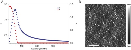
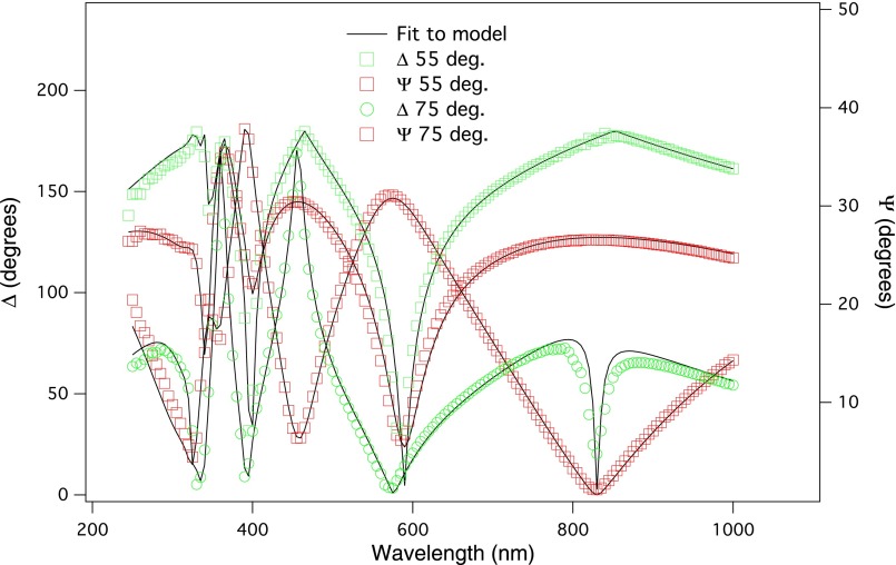
Characterization of the optical properties of our amorphous TiO2 shows that it is an ideal material for DMs. Fig. 1A shows the measured optical properties of a TiO2 film from UV (243 nm) to near-infrared (1,000 nm) wavelengths. To extract the TiO2 optical properties from the collected data, we used a Tauc−Lorentz (TL) oscillator model developed for amorphous materials (21). Over the visible spectrum, the refractive index ranges from 2.63 to 2.34 and remains relatively flat between λ = 500 nm and λ = 750 nm (Δn = 0.09). Below the wavelength of 500 nm, the index of refraction increases rapidly, implying the approach of an electronic transition. For wavelengths shorter than 360 nm, the imaginary part of the refractive index, k, begins to take on nonzero values, a result of interband absorption. From the ellipsometry data and corresponding TL model, we determine the bandgap, Eg, to be 3.456 eV [the full set of fitting parameters (Table S1) and raw ellipsometry data (Fig. S1) are included in Supporting Information]. This value of the bandgap is in good agreement with previously reported values for amorphous TiO2 (22).
Fig. 1.
Amorphous titanium dioxide material properties. (A) Measured real (blue squares) and imaginary (red circles) part of the refractive index (n and k) as a function of wavelength. The full set of ellipsometry data used in obtaining these optical functions is included in Supporting Information. (B) Atomic force microscope image of a typical TiO2 film deposited via ALD. The film is an atomically smooth surface with RMS roughness of 0.738 nm.
Table S1.
Fitting parameters for TiO2 film
| Parameter | Value |
| Thickness, nm | 67.43 ± 0.0342 |
| A, eV | 422.4 ± 18.4 |
| E0, eV | 3.819 ± 0.0304 |
| C, eV | 1.434 ± 0.0294 |
| Eg, eV | 3.456 ± 0.00791 |
Fig. S1.
Raw ellipsometry data used to determine the TiO2 optical constants, Ψ and Δ, for the TiO2 film on a silicon substrate as a function of wavelength. The green squares and circles are the values of Δ for angles of 55° and 75°, respectively. The red squares and circles are the Ψ values for angles of 55° and 75°, respectively. The black lines are generated data from the model described in Optical Characterization.
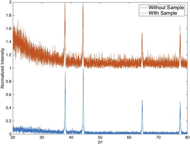
Our TiO2 films also exhibit surface roughness that is much smaller than the incident wavelength, as characterized by atomic force microscopy (AFM). Fig. 1B shows an AFM scan of a typical TiO2 film deposited on a fused silica substrate. The scan has a root mean square (RMS) roughness of 0.738 nm, which is on the order of the surface roughness of the underlying substrate (Fig. S2). Due to the absence of grain boundaries verified by AFM, coupled with the X-ray diffraction data (Fig. S3), we conclude that the material is amorphous. The measured roughness of the amorphous TiO2 is an order of magnitude less than other phases such as polycrystalline rutile or anatase (20). The latter two phases generally have grain boundaries and RMS roughness as high as 5–10 nm, both of which contribute to light-scattering loss (23).
Fig. S2.
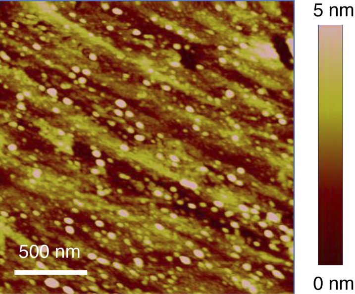
Atomic force microscope image of bare glass substrate with a root-mean-squared roughness of 0.698 nm.
Fig. S3.
X-ray diffraction of ALD TiO2. There are no observable diffraction peaks from any TiO2 polymorphs (red line). The peaks that appear in the scan result from the X-ray diffraction stage as can be seen from comparing the scan with (red) and without (blue) the sample.
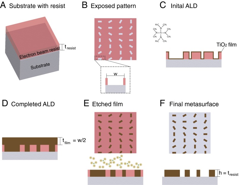
To achieve highly efficient metasurface devices while preserving the optical properties of ALD-prepared TiO2, we used the fabrication process shown in Fig. 2. We spun electron beam resist (EBR) onto a fused silica substrate to produce a layer with thickness, tresist (Fig. 2A). Control of tresist is important because it sets the height of our final nanostructures. We patterned the resist using electron beam lithography and subsequent development in solution to remove the exposed EBR. This pattern is the inverse of our final metasurface (Fig. 2B). We transferred the exposed sample to an ALD chamber set to 90 °C. The purpose of this temperature is twofold: It produces the desired amorphous phase and keeps the EBR below its glass transition temperature (i.e., prevents deterioration of the nanoscale patterns). During the deposition, the gaseous TiO2 precursor (TDMAT) coated all exposed surfaces, producing a conformal film on the top and side of the EBR as well as on the exposed fused silica substrate (Fig. 2C). We allowed the ALD process to reach a specific thickness such that all features had been completely filled with TiO2. Because the conformal ALD process fills exposed features from both sides, the total ALD film thickness required is tfilm ≥ w/2, where w is the maximum width of all gaps (Fig. 2D). In practice, we allowed the deposition to proceed well beyond the minimum requirement of half the feature width to ensure that TiO2 had sufficiently diffused into all pores and that there are no voids in the final nanostructures. We removed the residual TiO2 film that coats the top surface of the resist by reactive-ion-etching the sample in a mixture of BCl3 and Cl2 gas (8:2), similar to a planarization technique. The etch depth was equal to tfilm so that the etching process exposes the underlying resist and the top of the nanostructures (Fig. 2E). We removed the remaining resist and left only the nanostructures that make up our metasurface (Fig. 2F). In this way, we obtained structures of heights tresist while only needing to deposit a film of thickness tfilm ≈ w/2, which is timesaving and efficient.
Fig. 2.
Fabrication process for DMs. (A) EBR on fused silica (or equivalent transparent substrate) with thickness tresist that ultimately sets the height of the final structure (perspective view). (B) Inverse of the final metasurface pattern imprinted into the EBR by electron beam lithography and subsequent development of the pattern (top view). The boxed area is an expanded cross-section of the maximum feature width, w. (C) Initial TiO2 deposition via ALD conformally coats sidewalls and top of the EBR and exposed substrate (side view). TDMAT molecule used for ALD is also shown. (D) Completed deposition of the TiO2 yields a film thickness greater than half the width of the maximum feature size, tfilm ≥ w/2. (E) Exposed tops of the TiO2 metasurface and residual EBR after reactive ion etching with a mixture of Cl2 and BCl3 ions (top and side view). (F) Final DM after removal of remaining EBR (top and side view).
We note that this approach is different from standard liftoff techniques, as one cannot use conventional liftoff process due to the conformal coating of the ALD films. In addition, creating high-aspect ratio nanostructures via dry etching of TiO2, similar to other dielectric materials, is difficult and can lead to increased sidewall roughness. This ALD process is different from previous techniques (24, 25) where the patterns created are generally fixed by a set template (e.g., anodic alumina or inverse opal). Here we are free to define more complex nanostructures because we use ALD directly on exposed EBR.
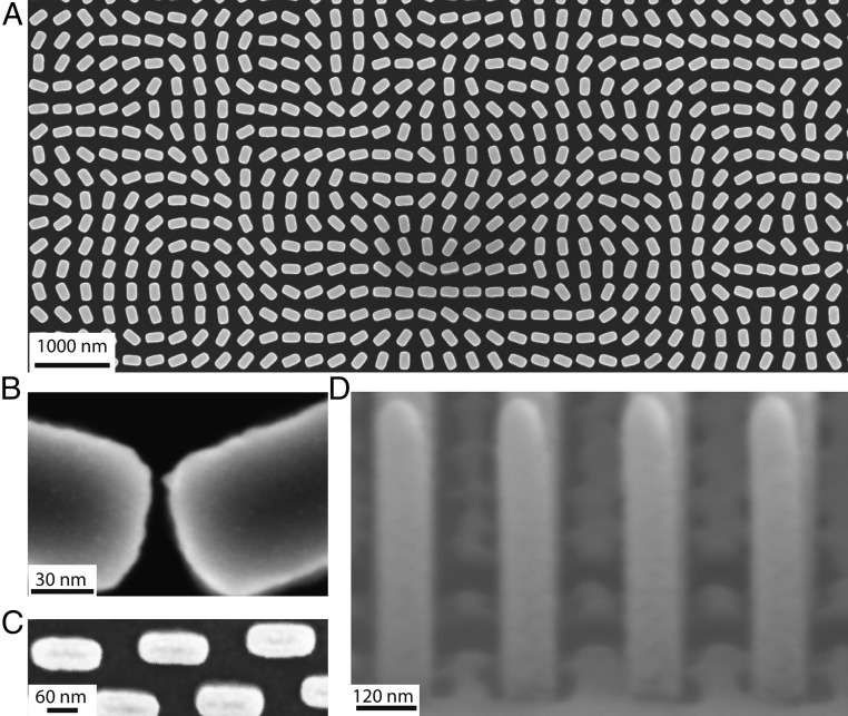
Investigation of the structures, fabricated using the process above, shows that we produce nanostructures (nanofins) with the desired anisotropy and subwavelength dimensions. Fig. 3 shows SEM images of a fabricated metasurface hologram. As seen in Fig. 3A, we can densely pattern large areas with subwavelength-spaced TiO2 nanofins. This ultimately ensures that the majority of the incident light is imprinted with a desired phase, higher diffraction orders are suppressed, and we can produce, in our case, holographic images with high efficiency. Fig. 3B shows an SEM of the metasurface at high magnification, allowing resolution of individual nanofins. With this process, we can also obtain extremely small spacing between individual nanofins, as shown by the 6-nm gap in Fig. 3B. The structures in this case have dimensions of 250 nm × 90 nm, but we can produce structures with dimensions as small as 40 nm (Fig. 3C).
Fig. 3.
Scanning electron microscope images of fabricated structures. (A) Large-scale view of a fabricated metasurface hologram composed of TiO2 nanofins. (B) Zoomed top view of the metasurface showing individual nanofins. The fabricated nanofins are free from residual resist and have dimensions ±10 nm of the designed dimensions of 250 nm × 85 nm. It can also be seen that, with this fabrication technique, we can achieve gaps between structures as small as 6 nm. (C) Top view of structures with lateral dimensions of ∼40 nm. (D) Cross-section (side view) of nanofins exhibiting vertical sidewalls with a height of ∼600 nm. The oscillations in contrast between nanofins result from shadowing effects during deposition of a metal film used to prevent charging while we image the samples.
Structures that deviate from 90° sidewalls, taking on a more triangular cross-section, can introduce phase errors in the metasurface. Similarly, structures with large voids or defects will reduce the effective refractive index of the nanofins. Fig. 3D shows a cross-section SEM of the nanofins (vertical direction in the image is the direction of light propagation). We observe that the angle of the structures in the vertical direction is 89°; that is, the nanostructures are highly anisotropic. This anisotropy is despite the fact that the nanostructures shown here are relatively tall compared with their other dimensions, with heights of 600 nm. Similarly, we do not see any void formation in the center of the nanofins. From the SEMs, it can also be seen that the final nanostructures have minimal surface and sidewall roughness.
To demonstrate the efficiency and functionality of our TiO2 metasurfaces, we designed three metasurface holograms (metaholograms) to have peak efficiencies at wavelengths of 480, 532, and 660 nm. We impart the required phase via rotation of the birefringent TiO2 nanofins shown in Fig. 3—known as geometric or Pancharatnam−Berry (PB) phase (26–28). (For more detail on this technique, see refs. 1 and 27, Materials and Methods, and Supporting Information). An advantage of the PB phase is that the imparted phase is wavelength-independent (only the efficiency changes with wavelength), thus providing an ideal platform to test the performance of our metasurface over the entire visible range. We compute the phase map of a holographic image, the binary Harvard logo, by means of the Gerchberg−Saxton phase-retrieval algorithm (29) (Fig. S4).
Fig. S4.
Phase map of Harvard logo used to generate holograms for design wavelength of 480 nm. Inset shows a 150 × 150 pixel phase distribution. This phase information was translated to pillar rotations.
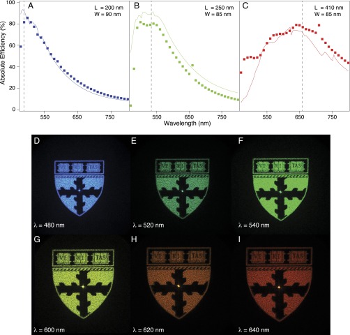
Fig. 4 A−C shows the measured and simulated efficiencies as a function of wavelength from 480 nm to 800 nm for the metaholograms designed at λ = 480, 532, and 660 nm, respectively. (Figs. S5 and S6 show simulated field profiles and transmission for the nanopillars.) We define absolute efficiency as the total optical power of the reconstructed Harvard logo divided by the optical power measured through a 300 × 300 μm2 square aperture, which is the same size as the hologram (see Materials and Methods and Fig. S7 for measurement details). The experimental results generally follow the simulation data and reach maxima of 82, 81, and 78% near the design wavelengths of 480, 532, and 660 nm, respectively. These values are, to our knowledge, the highest reported to date, even compared with reflective metasurfaces (16, 30, 31).
Fig. 4.
Measured absolute efficiencies and holographic images. (A−C) Measured (square markers) and simulated (solid line) hologram efficiencies. We define the absolute efficiency as the ratio of the total optical power of the hologram to the total optical power transmitted through an aperture of the same size as the hologram (300 × 300 μm2). The vertical dashed line marks the design wavelengths of each device, and device dimensions are (A) 200 nm × 90 nm, (B) 250 nm × 85 nm, and (C) 410 nm × 85 nm. (D−I) Holographic images covering the visible spectrum. The input wavelength is (D) 480 nm, (E) 520 nm, (F) 540 nm, (G) 600 nm, (H) 620 nm, and (I) 640 nm. All images were obtained from the device designed for 480 nm and show the broadband behavior of a single device. The bright spot in the center of the image is due to the propagation of zero-order light.
Fig. S5.
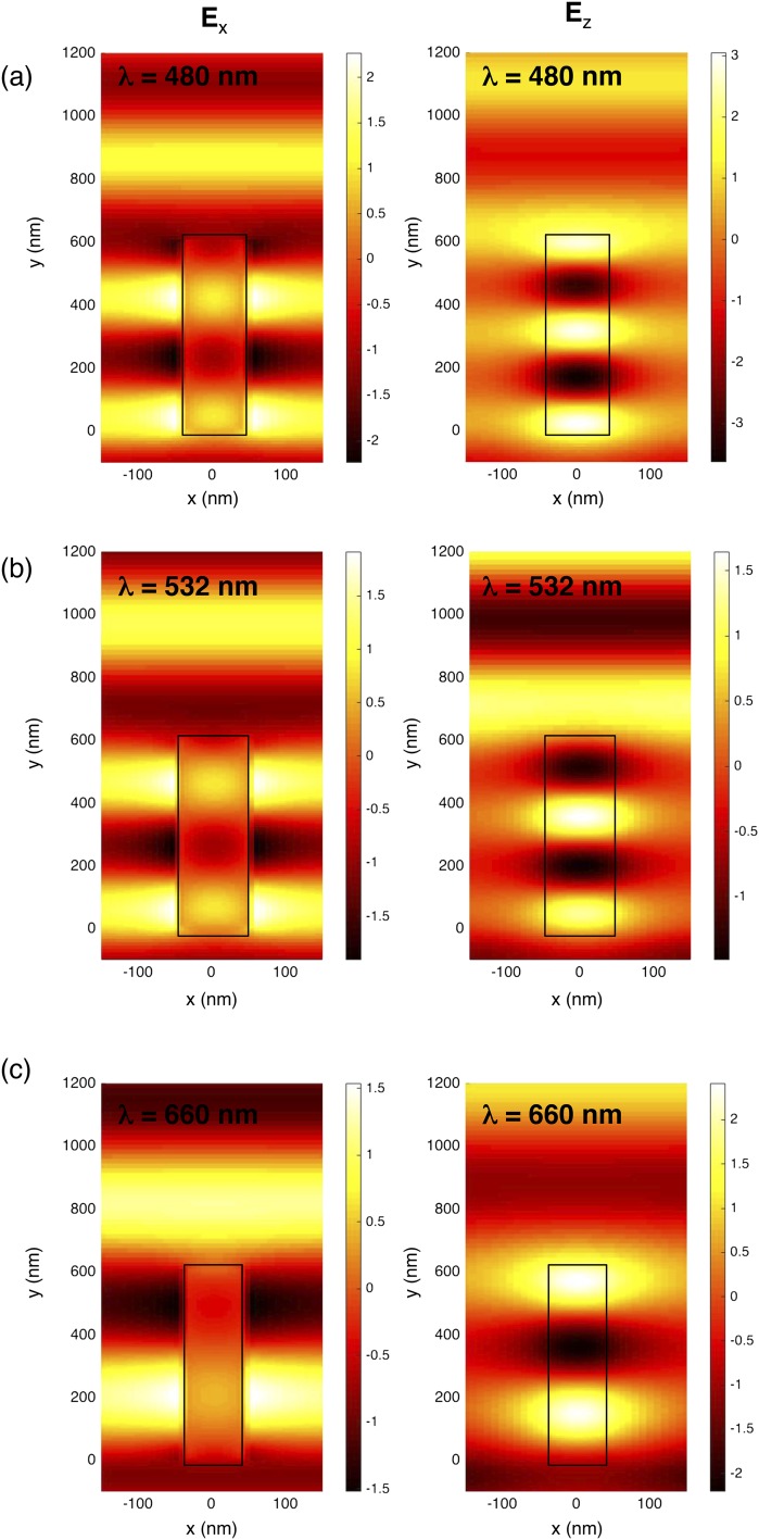
Simulated electric field profiles at design wavelength. Real part of the x component (Left) and z component (Right) of the electric field at design wavelengths (A) 480 nm, (B) 532 nm, and (C) 660 nm. All fields are shown through a cross-section of the nanofin width, and the nanofin is highlighted in each panel with a black box. One can see that the x and z components of the electric fields exiting the pillar, at each wavelength, are out of phase by π radians, as required for PB phase. The TiO2 pillars are simulated on a glass substrate that occupies the half space below y = 0, and the wave propagates in the +y direction.
Fig. S6.
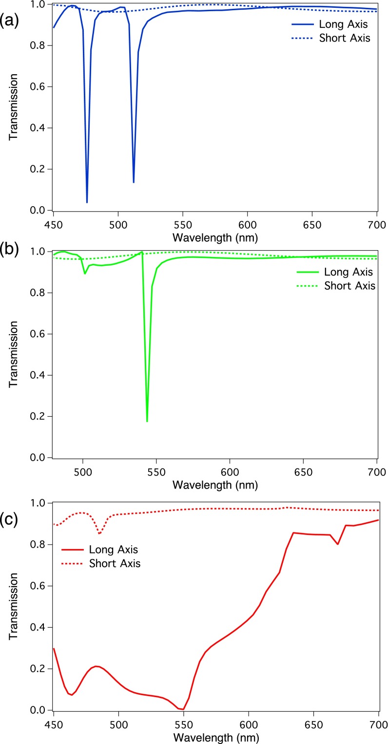
Simulated transmission spectra for TiO2 nanofins on a periodic lattice at design wavelengths of (A) 480 nm, (B) 532 nm, and (C) 660 nm. In each panel, the solid (dashed) line corresponds to an incident plane wave source polarized along the long (short) axis of the rectangular nanofins.
Fig. S7.
Schematic of measurement setup for collecting holographic images. LP, linear polarizer; λ/4, quarter waveplate; SuperK, Supercontinuum laser.
We note that, in certain cases, there are discrepancies between the simulated and measured trend. Differences between designed and fabricated nanofin dimensions and the possibility of weak coupling between fins likely cause these discrepancies. Additionally, the total efficiency of a geometric phase device depends on the transmission for an electric field polarized along the long or short axis of the individual elements (32). We see high transmission through the elements (Fig. S6), especially near the design wavelengths, but these transmission values could be further increased by exploring antireflective coatings or by impedance matching techniques.
Because the geometric phase is a wavelength-independent effect, we can generate holographic images across the visible spectrum from a single design. Fig. 4 D−I shows the holographic images across the visible spectrum for the hologram with a design wavelength of 480 nm. The subwavelength spacing and oversampling of the phase map can be seen in the images because there is sharp resolution of fine features such as the word “VERITAS” at the top of the Harvard crest. The bright spot near the center of the cross of the Harvard logo is from the zero order. However, at the design wavelength, the ratio of the intensity in the zero order to the total intensity contained in the hologram image is ∼1%.
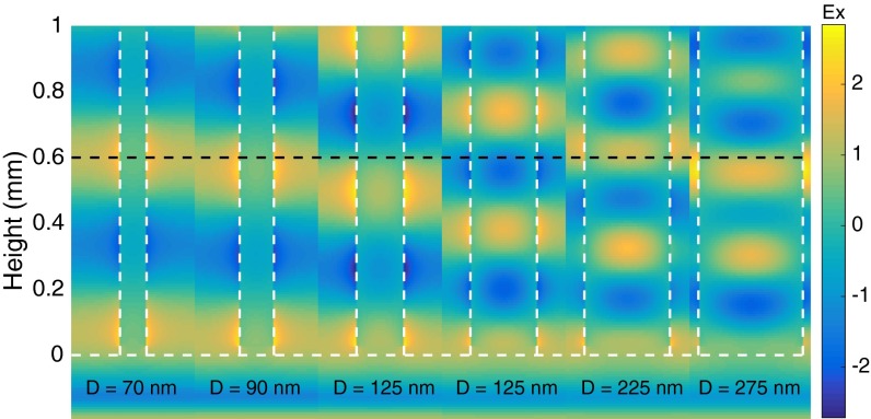
Although we have chosen to demonstrate our process using PB-phase metaholograms, the TiO2 properties and fabrication process are not limited to this specific type of metasurface. For example, simulations using the measured optical constants of our TiO2 and structural dimensions achievable with our fabrication process show that we can vary pillar dimensions to provide full 2π-phase coverage rather than using the geometric phase (Fig. S8). Thus, one can also use the results we presented here to produce DMs that use linear birefringent resonators to encode phase information (5). Moreover, the demonstration of full 0- to 2π-phase coverage enables the implementation of any DM components with high efficiency at visible wavelengths such as axicons, lenses, gratings, and polarization beam splitters.
Fig. S8.
Simulation of full 2π-phase coverage using TiO2 nanopillars with varied diameters. The white dashed lines show the placement of the TiO2 nanopillars, and the diameter of each pillar is listed below. Around each pillar, a 325-nm cross-section of the x component of the electric field is included. The black dashed line is set to 600 nm, the height of the nanofins that we presented in the main text.
We have detailed the experimental realization of highly efficient DMs that span the visible spectrum. We used ALD to produce smooth amorphous TiO2 films that are transparent for wavelengths longer than 360 nm and have an index of refraction that is sufficiently high to provide complete phase control over an optical wavefront. The fabrication technique for these metasurfaces, requiring only single-step lithography, provides a simple method to produce the highly anisotropic nanostructures that are necessary for DMs. Although we used TiO2, our process is applicable to any material that can be deposited via ALD. The fabricated metasurface holograms have the highest recorded efficiencies to date (82, 81, and 78%) at their respective design wavelengths. The technique presented here is general and can be applied to any type of metasurface. Careful consideration of the optical properties of our base material and the precision of the fabrication technique allowed us to expand the utility of DMs to visible wavelengths. This work can enable the creation of new compact optical systems with thicknesses that are orders of magnitude less than traditional optical systems.
Materials and Methods
Device Fabrication.
All devices used above were fabricated on an f-silica substrate. Substrates were first coated with hexamethyldisilazane to promote resist adhesion followed by spin coating of undiluted positive-tone EBR (ZEP-520A; Zeon Chemicals). For the devices shown, we spun the resist at 1,750 rpm to achieve the desired resist thickness of 600 nm. The resist was then baked at 180 °C for 5 min. Subsequently, samples were coated with 10 nm of chromium via electron beam evaporation to avoid charging effects during the writing process. The patterns were exposed using an accelerating voltage of 125 kV (ELS-F125; Elionix Inc.) and developed in o-xylene for 60 s under gentle agitation. For the ALD (Savannah; Cambridge Nanotech) of TiO2, a standard two-pulse system of water and the TDMAT precursor was used with a 0.2-s water pulse followed by a 7-s delay and a 0.4-s TDMAT pulse followed by a 10-s delay. The system was left under continuous 20 cm3/min flow of N2 carrier gas and was maintained at 90 °C throughout the process. This led to an overall deposition rate of ∼0.7 nm per cycle. Reactive ion etching was carried out on Unaxis inductively coupled plasma (ICP) reactive ion etching with a mixture of Cl2 and BCl3 gas (3 and 8 cm3/min, respectively) at a pressure of 4 mTorr, substrate bias of 150 V, and ICP power of 400 W. Etch rates were typically between 1.3 nm/s and 1.6 nm/s. After processing was complete, the samples were exposed to UV irradiation and ozone, followed by soaking in Remover PG (MicroChem Corporation) for 24 h.
Device Design and Simulation.
We translate the computed phase map, φ(x, y), into a spatial distribution of angles, θ(x, y) = φ(x, y)/2, that sets the rotation angle of a given nanofin at position (x, y). The size of each metahologram is 300 × 300 μm2, consisting of 600-nm-tall TiO2 nanofins. Simulations were performed using 3D finite-difference time-domain method (FDTD; Lumerical Inc.). The nanofin’s height, width, and length were optimized to provide a π-phase shift between its major and minor axis, which is required to achieve maximum conversion efficiency based on the geometrical phase (see Figs. S5 and S6 and surrounding discussion).
Device Measurement.
Devices were characterized using the setup shown in Fig. S7 consisting of a fiber-coupled laser source (supercontinuum laser; NKT Photonics), linear polarizers, quarter waveplates, a lens, and a camera/detector. All measurements were carried out using circularly polarized light as required for PB phase. A linear polarizer and quarter waveplate at the input generated the circularly polarized light, and the set of quarter waveplate and linear polarizer at the output filtered out unconverted light—light whose helicity is the same as the input light.
Optical Characterization
We deposit blanket TiO2 films via ALD onto silicon substrates to prepare samples for spectroscopic ellipsometry (SE) measurements. When more than one material is present for SE measurements, a model must be developed to extract the complex refractive index, , of a specific layer. In our case, we use a standard model for the substrate, and we apply the TL model for amorphous materials to the TiO2 film.
The TL model that we use to extract the optical constants of our ALD TiO2 is a combination of the normal quantum mechanical Lorentz oscillator and the model Tauc derived for the imaginary part of the dielectric constant for amorphous materials above the bandgap. Tauc derived this model assuming a set of N noninteracting oscillators per unit volume and arrived at the following expression for the imaginary dielectric constant:
| [S1] |
where AT is the amplitude of the oscillator and Eg is the transition energy.
For the Lorentz oscillator, the imaginary part of the dielectric function is given by
| [S2] |
with being the resonanto energy of the oscillator and C accounting for broadening. Jellison and Modine (21) combined Eq. S1 and Eq. S2 to account for shortcomings present in each model, leading to the TL model for the dielectric constant (1)
| [S3] |
where A is the product of AT and AL; we have defined the other fitting parameters above. The real part of the dielectric function is then obtained through Kramers−Kronig integration. The values of the four fitting parameters as well as the thickness of the film are shown in Table S1. Fig. S1 shows the raw ellipsometry data Ψ and Δ, and the corresponding generated data based on the model discussed above.
Structural Characterization
As stated in in the main text (discussion surrounding Fig. 1B), the measured surface roughness of the TiO2 films is on the order of surface roughness of the underlying substrate. Fig. S2 shows an AFM scan of the fused silica substrates used throughout this study. From the image, we extract an RMS roughness of ∼0.600 nm. This value is comparable to the measured surface roughness of a fused silica substrate with a film deposited on top (0.738 pm).
To determine the atomic structure of the ALD TiO2, we use X-ray diffraction (D8 Discover; Bruker). As can be seen from Fig. S3, there are no signs of any diffraction peaks from TiO2, even over the large-angle scan. We measure this diffraction spectrum for a TiO2 film on a 1-inch-diameter fused silica substrate and align the substrate to the center of the X-ray beam via a laser alignment mark. The absence of diffraction peaks indicates that the TiO2 films that we deposit are amorphous. In contrast, if the film was polycrystalline, the different polymorphs would generate diffraction peaks at 27.35° for rutile or ∼25° for anatase, for example.
Geometric Phase
We use PB (2–4) phase optical elements to implement the holograms, as first detailed by Bomzon et al. (1). In our case, the individual elements are TiO2 nanofins that act as discrete uniaxial crystals—they possess a structural birefringence that leads to a fast and slow optical axis, which introduces a phase difference between orthogonal components of the incident electrical field. It is then a spatially varying rotation of the fast axis of each nanofin that gives rise to the geometric phase accumulation, as detailed by Pancharatnam (26) and Berry (27). Mathematically, in Jones calculus, a waveplate with spatially varying fast axis, in the basis of left and right circularly polarized light (LCP and RCP, respectively), can be represented by the matrix (5)
| [S4] |
where is the retardance of the waveplate and represents angle of rotation of a waveplate at position . The matrix above allows one to take a beam of arbitrary input polarization, , and find the output state
| [S5] |
where and represent the left and right circularly polarized basis vectors and is the projection of the input polarization onto the RCP and LCP basis, respectively. As shown by Bomzon et al. (1), a particular case of interest occurs when the polarization of the input beam is RCP or LCP and the retardation, , is π. In this particular case, the efficiency of the system goes to unity, and the output state for an input of RCP light becomes
| [S6] |
which shows that the output polarization is the inverse of the input polarization and the output of the beam has acquired a phase of . By the symmetry of the half waveplate, the angle can only vary from 0 to π, but the additional geometric of 2 means that, by locally rotating the TiO2 nanofins, we can achieve full 2π-phase coverage.
Metahologram Design, Simulation, and Measurement
To create the holographic images shown in Fig. 4, we first take a binary image and produce a phase map via the Gerchberg−Saxton algorithm (Fig. S4). We then run simulations (3D FDTD; Lumerical), using the measured TiO2 optical data shown in Fig. 1A. At a fixed height of 600 nm, we optimize the length and widths of the nanofins to provide the π-phase difference between two orthogonal components of the electric field (Ex and Ez), as required for maximum efficiency. As can be seen from Fig. S5, at the design wavelengths of 480, 532, and 660 nm, the TiO2 nanofins provide a π-phase delay between the x and z components of the electric field and thus act as a half waveplate.
Although each individual nanofin must introduce a π-phase shift to have a maximum conversion efficiency (ratio of power in the output circular polarization and the power in the input circular polarization with opposite handedness), the total efficiency of the devices also depends on the transmission of each of the nanofins (5, 6). Fig. S6 shows the simulated transmission spectra of the TiO2 nanofins used for design wavelengths of 480, 532, and 660 nm. The simulations were run with a source polarized parallel to the long or the short axis, and the simulation setup is identical to that used in Fig. S5. The transmission remains relatively high for most designs throughout the entire visible. However, the design for 660 nm has relatively low transmission at shorter wavelengths; this is reflected in the measured efficiency and could be amended by allowing the optimization algorithm of the structures to search more exhaustively for a structure with higher transmission. Additionally, one could include antireflective coatings, taper the nanofins, or explore using overlapping electric and magnetic resonances (Huygens metasurfaces) to maximize the efficiency of all devices; this is beyond the scope of the current work.
We collect the holographic images shown in Fig. 4 using the schematic shown in Fig. S7. A supercontinuum laser provides access to wavelengths from ∼470 nm to 800 nm and is sent through a collimator, linear polarizer, and quarter waveplate to inject circularly polarized light, as required by the PB phase (see discussion in Geometric Phase). The circularly polarized light is then incident on the 300 × 300 μm2 metahologram contained on the sample and is converted to a holographic image with the opposite handedness of the input light. The light that passes through the sample is then sent through a 100× objective with a numerical aperture of 0.9. Because the spot of the collimated beam is larger than the area of the hologram, as well as to filter out any light that passes through the hologram but does not get converted (due to the TiO2 nanofin not working as a perfect half waveplate, for example), we place a filter in cross-polarization with respect to the input light after the objective. In the case of efficiency measurements, the intensity is then measured using a power meter. For the case of collecting the holographic images, we pass the light through a Bertrand lens to magnify the hologram.
Simulations for General TiO2 Metasurface
The process and TiO2 material properties demonstrated in Fig. 1A are not limited to metasurfaces implemented using PB phase. To show that we can produce different types of metasurfaces, e.g., those shown by Arbabi et al. (5), we simulate structures with the collected n and k data of our TiO2 and nanostructure dimensions achievable with our process. The simulation results are shown in Fig. S8. As we vary the diameter of a TiO2 pillar, fixed at a height of 600 nm, we can produce phase differences from 0 to 2π without using geometric phase.
Acknowledgments
We thank A. Zhu, J. P. B. Mueller, A. A. High, and A. Dibos for useful discussion. This work was supported by Charles Stark Draper Laboratory, Inc. (SC001-0000000959) and the Air Force Office of Scientific Research (FA9550-14-1-0389) MURI Grant. R.C.D. is supported by a fellowship through Charles Stark Draper Laboratory, Inc. W.T.C. acknowledges a postdoctoral fellowship from Ministry of Science and Technology, Taiwan (104-2917-I-564-058). This work was performed, in part, at the Center for Nanoscale Systems (CNS), a member of the National Nanotechnology Infrastructure Network, which is supported by the National Science Foundation (NSF) under NSF Award ECS-0335765. CNS is part of Harvard University.
Footnotes
Conflict of interest statement: A part of the current work has been submitted for a provisional patent.
This article contains supporting information online at www.pnas.org/lookup/suppl/doi:10.1073/pnas.1611740113/-/DCSupplemental.
References
- 1.Bomzon Z, Kleiner V, Hasman E. Pancharatnam−Berry phase in space-variant polarization-state manipulations with subwavelength gratings. Opt Lett. 2001;26(18):1424–1426. doi: 10.1364/ol.26.001424. [DOI] [PubMed] [Google Scholar]
- 2.Lin D, Fan P, Hasman E, Brongersma ML. Dielectric gradient metasurface optical elements. Science. 2014;345(6194):298–302. doi: 10.1126/science.1253213. [DOI] [PubMed] [Google Scholar]
- 3.Yang Y, et al. Dielectric meta-reflectarray for broadband linear polarization conversion and optical vortex generation. Nano Lett. 2014;14(3):1394–1399. doi: 10.1021/nl4044482. [DOI] [PubMed] [Google Scholar]
- 4.Aieta F, Kats MA, Genevet P, Capasso F. Multiwavelength achromatic metasurfaces by dispersive phase compensation. Science. 2015;347(6228):1342–1345. doi: 10.1126/science.aaa2494. [DOI] [PubMed] [Google Scholar]
- 5.Arbabi A, Horie Y, Bagheri M, Faraon A. Dielectric metasurfaces for complete control of phase and polarization with subwavelength spatial resolution and high transmission. Nat Nanotechnol. 2015;10(11):937–943. doi: 10.1038/nnano.2015.186. [DOI] [PubMed] [Google Scholar]
- 6.Khorasaninejad M, et al. Achromatic metasurface lens at telecommunication wavelengths. Nano Lett. 2015;15(8):5358–5362. doi: 10.1021/acs.nanolett.5b01727. [DOI] [PubMed] [Google Scholar]
- 7.Yu N, et al. Light propagation with phase discontinuities: Generalized laws of reflection and refraction. Science. 2011;334(6054):333–337. doi: 10.1126/science.1210713. [DOI] [PubMed] [Google Scholar]
- 8.Kildishev AV, Boltasseva A, Shalaev VM. Planar photonics with metasurfaces. Science. 2013;339(6125):1232009. doi: 10.1126/science.1232009. [DOI] [PubMed] [Google Scholar]
- 9.Yu N, Capasso F. Flat optics with designer metasurfaces. Nat Mater. 2014;13(2):139–150. doi: 10.1038/nmat3839. [DOI] [PubMed] [Google Scholar]
- 10.Zhan A, et al. Low-contrast dielectric metasurface optics. ACS Photonics. 2016;3(2):209–214. [Google Scholar]
- 11.Gutruf P, et al. Mechanically tunable dielectric resonator metasurfaces at visible frequencies. ACS Nano. 2016;10(1):133–141. doi: 10.1021/acsnano.5b05954. [DOI] [PubMed] [Google Scholar]
- 12.Lalanne P, Astilean S, Chavel P, Cambril E, Launois H. Design and fabrication of blazed binary diffractive elements with sampling periods smaller than the structural cutoff. J Opt Soc Am A Opt Image Sci Vis. 1999;16(5):1143–1156. [Google Scholar]
- 13.Sun S, et al. Gradient-index meta-surfaces as a bridge linking propagating waves and surface waves. Nat Mater. 2012;11(5):426–431. doi: 10.1038/nmat3292. [DOI] [PubMed] [Google Scholar]
- 14.Sun S, et al. High-efficiency broadband anomalous reflection by gradient meta-surfaces. Nano Lett. 2012;12(12):6223–6229. doi: 10.1021/nl3032668. [DOI] [PubMed] [Google Scholar]
- 15.Wen D, et al. Helicity multiplexed broadband metasurface holograms. Nat Commun. 2015;6:8241. doi: 10.1038/ncomms9241. [DOI] [PMC free article] [PubMed] [Google Scholar]
- 16.Zheng G, et al. Metasurface holograms reaching 80% efficiency. Nat Nanotechnol. 2015;10(4):308–312. doi: 10.1038/nnano.2015.2. [DOI] [PubMed] [Google Scholar]
- 17.Xie Q, et al. Atomic layer deposition of TiO2 from tetrakis-dimethyl-amido titanium or Ti isopropoxide precursors and H2O. J Appl Phys. 2007;102(8):083521. [Google Scholar]
- 18.George SM. Atomic layer deposition: An overview. Chem Rev. 2010;110(1):111–131. doi: 10.1021/cr900056b. [DOI] [PubMed] [Google Scholar]
- 19.High AA, et al. Visible-frequency hyperbolic metasurface. Nature. 2015;522(7555):192–196. doi: 10.1038/nature14477. [DOI] [PubMed] [Google Scholar]
- 20.Aarik J, Aidla A, Kiisler AA, Uustare T, Sammelselg V. Effect of crystal structure on optical properties of TiO2 films grown by atomic layer deposition. Thin Solid Films. 1997;305(1-2):270–273. [Google Scholar]
- 21.Jellison GE, Modine FA. Parameterization of the optical functions of amorphous materials in the interband region. Appl Phys Lett. 1996;69(3):371. [Google Scholar]
- 22.Eufinger K, Poelman D, Poelman H, De Gryse R, Marin GB. Photocatalytic activity of dc magnetron sputter deposited amorphous TiO2 thin films. Appl Surf Sci. 2007;254(1):148–152. [Google Scholar]
- 23.Apetz R, van Bruggen MPB. Transparent alumina: A light-scattering model. J Am Ceram Soc. 2003;86(3):480–486. [Google Scholar]
- 24.Sander MS, Cote MJ, Gu W, Kile BM, Tripp CP. Template-assisted fabrication of dense, aligned arrays of titania nanotubes with well-controlled dimensions on substrates. Adv Mater. 2004;16(22):2052. [Google Scholar]
- 25.King JS, Graugnard E, Summers CJ. TiO2 inverse opals fabricated using low-temperature atomic layer deposition. Adv Mater. 2005;17(8):1010–1013. [Google Scholar]
- 26.Pancharatnam S. Generalized theory of interference and its applications. Part I. Coherent pencils. Proc Indian Acad Sci A. 1956;44(5):247–262. [Google Scholar]
- 27.Berry MV. Quantal phase-factors accompanying adiabatic changes. Proc R Soc London A Math Phys Eng Sci. 1984;392(1802):45–57. [Google Scholar]
- 28.Bhandari R. Polarization of light and topological phases. Phys Rep. 1997;281(1):2–64. [Google Scholar]
- 29.Gerchberg RW. A practical algorithm for the determination of phase from image and diffraction plane pictures. Optik (Stuttg) 1972;35(2):237–246. [Google Scholar]
- 30.Ni XJ, Kildishev AV, Shalaev VM. Metasurface holograms for visible light. Nat Commun. 2013;4:2807. [Google Scholar]
- 31.Chen WT, et al. High-efficiency broadband meta-hologram with polarization-controlled dual images. Nano Lett. 2014;14(1):225–230. doi: 10.1021/nl403811d. [DOI] [PubMed] [Google Scholar]
- 32.Luo WJ, Xiao SY, He Q, Sun SL, Zhou L. Photonic spin Hall effect with nearly 100% efficiency. Adv Opt Mater. 2015;3(8):1102–1108. [Google Scholar]


