

A giant facet-dependent spin Hall conductivity is found in IrMn3 due to its chiral triangular antiferromagnetic structure.
Keywords: Spintronics, spin Hall conductivity, spin orbit torque, spin Hall angle, spin orbitronics, IrMn3, triangular antiferromagnet, antiferromagnet
Abstract
There has been considerable interest in spin-orbit torques for the purpose of manipulating the magnetization of ferromagnetic elements for spintronic technologies. Spin-orbit torques are derived from spin currents created from charge currents in materials with significant spin-orbit coupling that propagate into an adjacent ferromagnetic material. A key challenge is to identify materials that exhibit large spin Hall angles, that is, efficient charge-to-spin current conversion. Using spin torque ferromagnetic resonance, we report the observation of a giant spin Hall angle of up to ~0.35 in (001)-oriented single-crystalline antiferromagnetic IrMn3 thin films, coupled to ferromagnetic permalloy layers, and a that is about three times smaller in (111)-oriented films. For (001)-oriented samples, we show that the magnitude of can be significantly changed by manipulating the populations of various antiferromagnetic domains through perpendicular field annealing. We identify two distinct mechanisms that contribute to : the first mechanism, which is facet-independent, arises from conventional bulk spin-dependent scattering within the IrMn3 layer, and the second intrinsic mechanism is derived from the unconventional antiferromagnetic structure of IrMn3. Using ab initio calculations, we show that the triangular magnetic structure of IrMn3 gives rise to a substantial intrinsic spin Hall conductivity that is much larger for the (001) than for the (111) orientation, consistent with our experimental findings.
INTRODUCTION
Spin-orbitronics is an emerging field of current interest in which spin-orbit coupling gives rise to several novel physical phenomena, many of which also have potential technological significance (1, 2). Of particular interest is the spin Hall effect in which conventional charge current densities (JC) are converted to pure spin current densities () via spin-orbit coupling within the material (3, 4). The conversion efficiency is described by the spin Hall angle (SHA) θSH = eJS/JC. One of the most widely used techniques to measure SHA is by comparing the antidamping spin torque generated by a radio frequency (RF) spin current that propagates into an adjacent ferromagnetic layer with the field torque generated by an RF charge current (2, 5–9). This technique of spin torque ferromagnetic resonance (ST-FMR) yields an effective SHA, (because, as we discuss further below, there can be other potential sources of spin current). The largest values of in conventional metals that have been reported to date include the heavy metals β-tantalum (2), β-tungsten (7), platinum [once the interface transparency is taken into account (9)], and bismuth-doped copper (10).
A prerequisite for large θSH is significant spin-orbit coupling. Of potential interest are compounds such as Ir1−xMnx, which are antiferromagnetic for various ranges of x. These compounds are widely used in spintronic devices because of the exchange bias fields that they imprint on neighboring ferromagnetic layers that lead to a unidirectional magnetic anisotropy (11). Theoretical studies predict that chemically ordered IrMn3 should exhibit a large anomalous Hall effect (AHE) due to its unusual triangular magnetic structure (12, 13), and recent experimental studies observed large AHE in the noncollinear antiferromagnets (AFs) Mn3Sn and Mn3Ge (14–16). Here, we observed a giant in Ir1−xMnx films and a large facet dependence of on IrMn3, which we find can be markedly enhanced by manipulating the populations of various AF domains via annealing in magnetic fields oriented perpendicular, but not parallel, to the film layers.
RESULTS
Microstrip devices, 10 μm wide and 100 μm long, are fabricated using standard optical lithography and ion milling techniques from Ir1−xMnx/permalloy (Py)/TaN films. The films are deposited by magnetron sputtering (see Materials and Methods for details) on Si(001) substrates (covered with 25-nm-thick SiO2), MgO (001) substrates, and Al2O3 (0001) substrates at room temperature (RT) in a high–vacuum deposition chamber. ST-FMR measurements are carried out by passing a high-frequency RF current into the device (JC is the charge current density in Fig. 1A) in the presence of an external field Hext that is applied in the plane at 45° to the microstrip. The charge current that flows in the Ir1−xMnx layer generates two distinct torques on the Py layer, namely, a spin-orbit torque and an Oersted field torque. The time derivative of the magnetization of Py is given by (5, 17)
| (1) |
where γ is the gyromagnetic ratio; is composed of the external field, the exchange bias field, and the out-of-plane demagnetization field; α is the Gilbert damping constant; is the Oersted field; is the spin current density generated in the Ir1−xMnx layer; μ0 is the permeability in vacuum; MS is the saturation magnetization of the Py layer, which is measured using vibrating sample magnetometry on the unpatterned film before device fabrication; t is the thickness of the Py layer; and is the direction of the injected spin moment. We note that JS represents any spin current that is generated by the passage of the charge current through the device that gives rise to an antidamping torque. As we discuss below, there may be mechanisms beyond the conventional spin Hall effect that generate spin currents in the device. The Oersted field depends on the RF current and the thickness of the Ir1−xMnx layer d and can be expressed as for our experiments, in which the Ir1−xMnx films are comparatively thin (10 to 150 Å).
Fig. 1. ST-FMR measurement of in p-IrMn3.
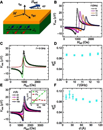
(A) Illustration of the ST-FMR experimental setup where Hext is the external field, M is the magnetization of the permalloy layer (yellow), and τH and τST are the torques on M due to the Oersted field created by the RF charge current and the spin current in the Ir1−xMnx layer (green), respectively. (B) ST-FMR spectra measured on a ~60 Å IrMn3/~60 Å Py sample at a frequency varying from 9 to 12 GHz. (C) ST-FMR spectrum measured at 9 GHz. The black solid lines are the fits with Lorentzian functions. The red and green solid lines represent the symmetric and antisymmetric Lorentzian fits, respectively. (D) Frequency dependence of measured of ~60 Å IrMn3/~60 Å Py. (E) ST-FMR spectra measured on these devices with different thicknesses of IrMn3 at 11 GHz. Inset: Thickness dependences of the symmetric and antisymmetric components of Vmix. (F) Thickness dependence of measured for IrMn3/~60 Å Py. Error bars correspond to 1 SD in (D) and (F).
Mixing the RF charge current through the device with the consequent oscillating magnetization of the Py layer, which affects the device resistance through its magnetoresistance, generates a dc voltage Vmix(Hext). Figure 1B shows typical ST-FMR spectra, that is, Vmix(Hext) as a function of Hext, measured on ~60 Å polycrystalline IrMn3 (p-IrMn3)/60 Å Py for RF frequencies varying between 9 and 14 GHz. As the RF frequency increases, the resonance field Hres increases, as expected from the Kittel model, and the magnitude of Vmix decreases. Vmix(Hext) has two components: an antisymmetric component due to the Oersted field–generated torque and a symmetric component that arises from the spin-orbit torque. The ST-FMR curves are fitted with symmetric and antisymmetric Lorentzian functions, according to (5, 9)
| (2) |
where c is a constant, VS and VA are the amplitudes of the symmetric and antisymmetric components, respectively, of the dc mixed voltage, and ΔH is the half linewidth. is given by (5, 9)
| (3) |
where Meff is the effective magnetization that can be extracted by fitting the resonance frequency fres as a function of Hres using the Kittel formula (18)
| (4) |
in which HB is the in-plane exchange bias field due to the interaction between Py and the IrMn3 layer. For p-Ir1−xMnx films, the measured in-plane exchange bias field is small compared to Hres.
Typical results of fitting the experimental data in Fig. 1B with Eq. 2 are shown in Fig. 1C, from which the fitting parameters VS, VA, Hres, and ΔH can be obtained. Using these parameters, is estimated to be 0.092 ± 0.003 (at 11 GHz) based on Eq. 3. exhibits little variation as a function of the RF excitation frequency (Fig. 1D). The dependence of the ST-FMR spectra on the thickness d of the p-IrMn3 layer is shown in Fig. 1E. From fits to these data using Eq. 2, the magnitude of VS varies little as a function of d, whereas VA increases approximately linearly with d (see inset to Fig. 1E), consistent with the larger Oersted field torques, as the RF charge current flowing in the p-IrMn3 layer increases. As shown in Fig. 1F, shows a weak dependence on d, which suggests that the spin diffusion length in IrMn3 is small (<~10 Å).
The magnitude of in p-IrMn3 is considerable (~0.1) and much larger than that of that was measured indirectly from spin pumping from permalloy into the Ir50Mn50 layer (19–21) but comparable to that found in spin pumping studies from yttrium iron garnet into Ir20Mn80 (22). To explore its origin, a systematic study of various Ir1−xMnx concentrations (x = 0, 0.17, 0.53, 0.64, 0.75, 0.80, 0.86, and 1) is carried out: the results are summarized in Fig. 2A for polycrystalline samples with ~60 Å–thick Ir1−xMnx layers that are coupled to 60 Å–thick Py films. The largest values of are found for x ~ 0.53, 0.64, and 0.75. The two end members show much smaller values and, perhaps surprisingly, are of opposite signs (~+0.03 for Ir and ~−0.02 for Mn). The dependence of on the thickness of Ir, Ir83Mn17, Ir47Mn53, Ir14Mn86, and Mn, respectively, is shown in fig. S1. These measurements indicate that the spin diffusion lengths in all of these metals are small (<~10 Å). We note that each of these films exhibits little variation as a function of the RF excitation frequency (fig. S2). Furthermore, we find no obvious correlation between the magnitude of and the in-plane exchange bias HB (Fig. 2B).
Fig. 2. Dependence of and HB on Mn concentration in Ir1−xMnx/Py bilayers.
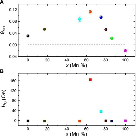
(A) measured at 11 GHz for polycrystalline bilayers of ~60 Å Ir1−xMnx/~60 Å Py versus the Mn concentration x. (B) In-plane exchange bias field for polycrystalline bilayers of ~60 Å Ir1−xMnx/~60 Å Py versus the Mn concentration x. Note that HB was measured after the films were annealed in an in- plane field of 1 T for 30 min at 300°C. Error bars correspond to 1 SD in (A).
We prepared films of IrMn3, oriented along the (001) and (111) facets, (see Materials and Methods) to explore the dependence of on the crystal orientation of the IrMn3. IrMn3 crystallizes in a face-centered cubic lattice (space group , no. 221). The magnetic moments of the Mn atoms are oriented within the (111) planes and form a triangular AF structure. The crystal orientations were determined by θ-2θ x-ray diffraction (XRD) and diffractograms from selected areas of transmission electron micrographs (Fig. 3). Growth of IrMn3 on (001) MgO and (0001) Al2O3 resulted in epitaxial IrMn3 layers with (001) and (111) facets, respectively. Growth of amorphous SiO2 on Si resulted in (111)-textured p-IrMn3 films. ST-FMR measurements as a function of RF frequency are summarized in fig. S3. For (111) IrMn3 and p-IrMn3, exhibits little dependence on the RF frequency, whereas for (001) IrMn3, is slightly higher at 9 and 10 GHz, which is attributed to a slightly poorer fit to the model when Hres is close to 0 Oe because of the small exchange bias field (fig. S4). Note that no signal is detected, as expected, in devices formed from IrMn3 films without any permalloy layers (fig. S4).
Fig. 3. Structural characterization of IrMn3.
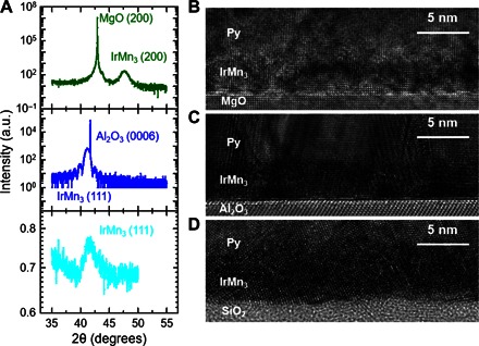
(A) The XRD measured on 100 Å (001) IrMn3 (blue line), (111) IrMn3 (cyan line), and p-IrMn3 films (black line). Each film is capped with a TaN layer with a thickness of 20 Å. (B to D) High-resolution transmission electron micrographs of 40 Å (001) IrMn3, (111) IrMn3, and p-IrMn3, with 60 Å Py/20 Å TaN capping layers.
Values of for (001)- and (111)-oriented IrMn3/Py films are summarized and compared to the results for p-IrMn3/Py bilayers in Fig. 4A. In all cases, depends weakly on the thickness of IrMn3 that ranges from ~30 to ~120 Å. A marked result is that the (001)-oriented structures exhibit much larger of ~0.20 compared to those exhibited either by p-IrMn3 or (111)-oriented IrMn3. Moreover, as shown in Fig. 4B, a significant facet dependence is observed for x ~ 75 and 80 atomic % (at %), but not for x ~ 53 and 64 at % (see fig. S5 for x-ray structural characterization). This is significantly different from a previous work on CuAu I–type AFs, which have collinear AF structures (21).
Fig. 4. Facet-dependent in crystalline Ir1−xMnx.
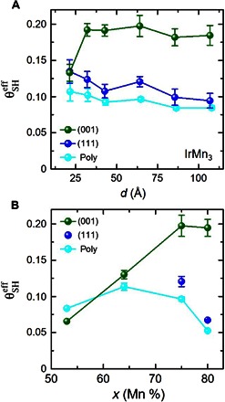
(A) as a function of IrMn3 thickness for (001)-oriented (olive circles), (111)-oriented (blue circles), and polycrystalline-oriented (cyan circles) films. (B) as a function of Mn concentration for (001), (111), and p-Ir1−xMnx. Error bars correspond to 1 SD in (A) and (B).
Our results show that the facet dependence of on IrMn3 is not correlated with the resistivity of the films (table S1). In any case, the fact that can be successively increased or decreased depending on the choice of anneal procedure rules out any correlation with the changes in the resistivity on annealing. Our observations are also not associated with the magnetizations of the permalloy layers, which are similar for (001), (111), and p-IrMn3 (fig. S6). Because the resistivity of the (001)-oriented IrMn3 is only 10 to 20% lower than that of (111) IrMn3, it seems very unlikely to account for the facet-dependent with a facet-dependent interface transparency. Furthermore, we find no correlation between the in-plane exchange bias HB and the magnitude of (Fig. 5). Here, HB is tuned by annealing the IrMn3-based devices in a 1-T magnetic field that is aligned parallel to the Py layers, and it was measured by two methods (fig. S7). Perhaps this is not surprising, because HB reflects the degree to which the magnetic moments within individual antiferromagnetic domains are uncompensated at the IrMn3/Py interface (23).
Fig. 5. In-plane exchange bias field and in crystalline Ir1−xMnx after annealing in in-plane magnetic field.
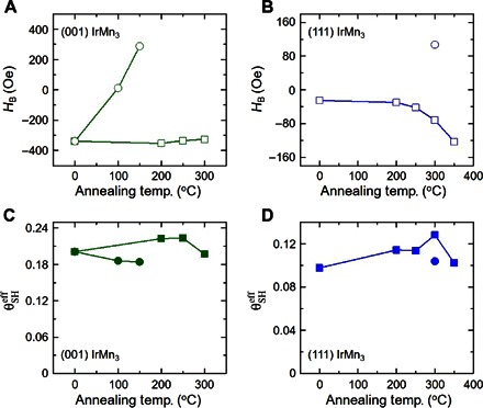
In-plane exchange bias field and as a function of annealing temperature for (001) IrMn3 (A and C) and (111) IrMn3 (B and D). The thickness of IrMn3 is 43 Å. Squares and circles indicate positive and negative in-plane magnetic field (1 T) during annealing (30 min), respectively.
Notwithstanding the lack of correlation of with HB, we find compelling evidence that the antiferromagnetic domain configuration of the Ir1−xMnx layer plays a key role in determining the magnitude of for x ~ 0.75 to 0.80. In a first set of experiments, IrMn3-based devices are annealed in a 1-T magnetic field at 300°C that is aligned perpendicular, rather than parallel, to the Py layers, as in the experiments described above. This field is large enough to cause the magnetization of the Py layer to be oriented nearly parallel to the field and thus perpendicular to the IrMn3/Py interface at 300°C. On cooling, the large perpendicular exchange field imposed by the Py moments in direct contact with the IrMn3 layer at the IrMn3/Py interface thereby influences the configuration of the AF domains within the IrMn3 layer, but only when the blocking temperature of the IrMn3 layer is below the anneal temperature. Remarkably, we find that perpendicular field annealing results in a marked increase of by almost a factor of two to ~35% for a (001) IrMn3/Py device, when the IrMn3 layer is ~3 nm thick (Fig. 6A). By contrast, of the corresponding (111) device is hardly changed (Fig. 6B). Subsequently, annealing the same (001)-oriented device in an in-plane magnetic field lowers , but then, annealing in a reverse perpendicular field (−1 T) recovers the higher value (Fig. 6A). The of the (111)-oriented device is barely affected by these annealing procedures (Fig. 6B). As shown in Fig. 6A, the increase in with perpendicular annealing is strongly dependent on the thickness of the IrMn3 (001) layer. When the IrMn3 layer is too thin or too thick, no effect is found. An enhancement in is found only for intermediate IrMn3 thicknesses in the range of 3 to 4 nm. This thickness dependence can be directly correlated with the thickness dependence of the blocking temperature (TB) of the antiferromagnetic structure of the IrMn3 layer. TB, a temperature smaller than the Néel temperature, reflects the temperature below which there is sufficient anisotropy to freeze the magnetization of the AF domains (24–26). The thickness dependence of HB for (001) and (111) IrMn3/Py–unpatterned films at RT is shown in Fig. 6C. This feature is also confirmed on the fabricated devices (fig. S8). No exchange bias is found for 2-nm-thick IrMn3 layers, consistent with TB being below RT (~200 K). Films that have a thickness ≥3 nm exhibit an exchange bias field at RT, and therefore, TB > RT. The 8-nm-thick film is sufficiently thick that TB is close to the bulk value (27) and, therefore, much higher than the annealing temperature (300°C). Thus, an important result is that is enhanced for perpendicular field annealing only when the AF structure of the IrMn3 layer can be reconfigured by exchange coupling with the Py layer when it is cooled from a temperature above its blocking temperature and cooled through this temperature to “block” the AF domains at RT. This field cooling–induced modification of the microscopic AF structure has previously been found using magnetic linear dichroism studies of in-plane field–annealed 50-nm-thick NiO layers that are exchange-coupled to ferromagnetic Co–Fe (28).
Fig. 6. Modulation of the in crystalline Ir1−xMnx after annealing in a perpendicular magnetic field.
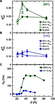
for (001) (A) and (111) (B) IrMn3/60 Å Py bilayers as a function of IrMn3 thickness measured sequentially in the following: an as-grown device, a device annealed in a 1-T perpendicular field (60 min), a device annealed in an in-plane 1-T field (30 min), and a device annealed in a −1-T perpendicular field (60 min). (C) Exchange bias field measured in (001) and (111) IrMn3/60 Å Py bilayers as a function of IrMn3 thickness after the unpatterned films were annealed in-plane in a 1-T field (30 min) using vibrating sample magnetometry. The annealing field was aligned along the (001) axis for the (001)-oriented samples. The exchange bias field was also measured in the same devices used in (A) and (B) via magnetoresistance measurements (see fig. S8). Error bars correspond to 1 SD in (A) and (B).
Note that when the exchange coupling between Py and IrMn3 is weakened by the insertion of Cu or Au layers, the Py layer will have less influence on the configuration of the AF domains in the IrMn3 layer. We find that decreases with increasing Au thickness for both (001)- and (111)-oriented devices to a facet-independent value when the Au layer is ~10 Å (fig. S9). For Cu spacer layers, decreases much more rapidly for devices with (001) orientation compared to those with (111) orientation, but a small difference in persists when the Cu layer is ~10 Å thick, likely because of the larger exchange interlayer coupling through Cu than through Au (29).
To summarize our annealing experiments, in-plane field annealing has no effect on the measured SHA for either (001)- or (111)-oriented IrMn3 samples, although the in-plane exchange bias field can be substantially changed in magnitude and direction. On the other hand, perpendicular field annealing substantially increases the SHA, independent of the direction of the perpendicular field. In both cases, it is to be expected that the occupancy of the various AF domains will be altered. The magnetic layer plays a critical role here: the external field orients the direction of the magnetization of the permalloy layer. The significant exchange interaction across the permalloy/AF interface layer can thereby be used to affect the occupation of the AF domains when these domains are above their blocking temperature. The magnetic field itself, at least for the magnitude of field accessible in our experiments, is not large enough to affect the AF domain structure or occupancy. Thus, annealing the IrMn3 layer by itself in an external field, when it is not exchange-coupled to permalloy, has no influence on the IrMn3 AF domain structure nor on the SHA, as we find in our experiments when we decouple the IrMn3 layer from permalloy by the insertion of thin Cu or Au layers. On the other hand, when the IrMn3 is in intimate contact with the permalloy, both in-plane and out-of-plane field annealing can influence the AF structure. For in-plane annealing, even though the AF structure is changed, for example, changing the in-plane exchange bias field, there is no effect on the SHA. Meanwhile, perpendicular field annealing does affect the SHA. We note that there could be a perpendicular exchange bias field, but we find that this is too small to be distinguished compared to the demagnetization field that dominates the out-of-plane field magnetic hysteresis loop. What is important for the spin orbit torques that act on the permalloy are spin currents that flow perpendicularly from the AF layer into the permalloy layer. We conjecture that this is why in-plane field annealing has no effect on the measured spin Hall conductivity (SHC) whereas perpendicular field annealing has a significant effect.
DISCUSSION
Our experiments suggest that there are two distinct contributions to : a first mechanism that is facet-independent and arises from bulk spin-orbit coupling within the IrMn3 layer, and a second mechanism that is strongly facet-dependent and is derived from the antiferromagnetic domains. IrMn3 is known to display a triangular chiral magnetic structure with the Mn magnetic moments aligned at 120° to each other in the (111) plane (27, 30) when Ir and Mn are chemically ordered. Recently, it was proposed that these structures will lead to an AHE, although they have no net magnetization (12, 13). Using ab initio calculations of the band structures and Berry curvatures (see Materials and Methods and the Supplementary Materials), we find that in addition to an AHE, the triangular AF structure also gives rise to an intrinsic SHC that is large and, moreover, is strongly facet-dependent (see Fig. 7 and table S2). Furthermore, the calculated SHC agrees very well with our experimental results. For a (111) IrMn3–oriented film, an in-plane current generates spin currents inside the (111) plane but negligible spin currents in the out-of-plane direction, whereas for the (001) film, the in-plane current leads to a large out-of-plane spin current whose amplitude is much larger than that of the (111) out-of-plane case.
Fig. 7. Chiral noncollinear antiferromagnetic orders and corresponding anomalous Hall conductivity and SHC.
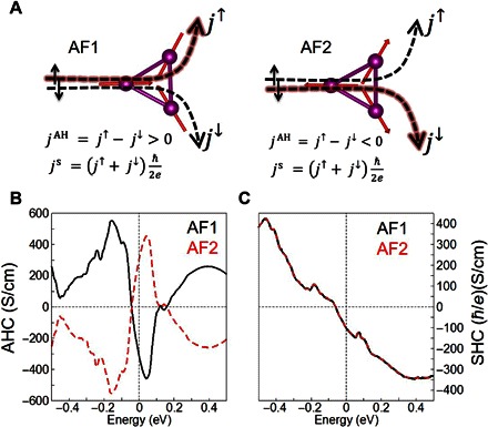
(A) Schematic diagram of two chiral AF orderings, AF1 and AF2, of the Mn moments in the (111) plane of IrMn3. As illustrated, spin-up and spin-down electrons feel opposite fictitious fields because of spin-orbit coupling. Thus, their trajectories will be in opposing transverse directions. Because of the underlying antiferromagnetic lattice, the induced transverse currents from opposite spins (j↑, j↓) are not equal in amplitude. Let us suppose that j↑ > j↓ for AF1. When reversing the spins, for example, by a time reversal operation, an opposite spin chirality is realized as AF2. The time reversal operation simultaneously reverses the spin and velocity. Thus, the deflection direction for the electron with a given spin does not change. However, the relative amplitude of these currents change, that is, j↑ < j↓, because of the inversed spin chirality. Therefore, AF1 and AF2 exhibit opposite anomalous Hall current jAH and the same spin Hall current js. (B and C) Ab initio calculations of the anomalous Hall conductivity (AHC) (σxy) and SHC with respect to chemical potential. The charge-neutral point is set to zero. Here, the x, y, and z axes correspond to the crystallographic directions , , and [111], respectively (see the Supplementary Materials). Because AF1 and AF2 can be transformed into each other by a mirror reflection or a time reversal operation, they exhibit opposite signs of AHC but the same sign of SHC.
In the cubic IrMn3 lattice, the Mn atoms are arranged in the form of triangles within the (111) plane of the primitive unit cell. Because of frustration, neighboring Mn moments align noncollinearly, at an angle of 120° to each other, to form two distinct AF arrangements, in which the Mn moments point toward (AF1) or out from the center of the triangle (AF2), respectively (see Fig. 7A). AF1 and AF2 can be transformed into each other by a mirror reflection or a time reversal operation. We note that mirror reflection, for example, with respect to the (110) crystallographic plane, should apply both to the lattice and magnetic moments and that time reversal only reverses directions of all moments. Because either the mirror symmetry or the time reversal symmetry is broken in IrMn3, AF1 and AF2 are nonequivalent ground states and are chiral images of each other. AF1 and AF2 exhibit the same energies and exist spontaneously in the real material. It is known that under time reversal, AHE is odd whereas spin Hall effect is even (31). Thus, we can conclude with the help of time reversal that AF1 and AF2 will exhibit the same SHC but opposite AHC. This intuition is fully consistent with our ab initio calculations (taking into account the numerical inaccuracies), as shown in Fig. 7 (B and C). In addition, each Mn exhibits a moment of 2.91 μB from our calculations, which is consistent with that of Chen et al.’s study (12). In addition, we calculate that there is a tiny out-of-plane net moment of 0.01 μB per Mn atom (along the [111] axis). This moment does not affect the values of SHC and AHC (as tested by setting this moment to zero and recalculating the results) but may be important in orienting the AF domains by perpendicular field annealing.
Our calculations show that the noncollinear AF order in the (111) plane generates a strong anisotropy of the SHC. Calculations of the SHC and AHC are shown in table S2 for the two cases where z is along [111] and [001]; the calculations correspond to our experiments. We define the SHC by , which is the spin current along the i direction generated by a charge current along the j direction, in which the spin polarization of the spin current is oriented along the k axis.
When the z axis is oriented along the [111] crystallographic direction and the x and y axes are aligned within the (111) plane, (in siemens per centimeter), thereby showing that an in-(111)-plane electric current can generate a considerable spin Hall current in the same plane. In contrast, the in-(111)-plane electric current generates a tiny spin current along the [111] direction: in this case, we find that (in siemens per centimeter).
We should point out that the shape of the SHC tensor depends on the coordinate system in which the directions of spin and currents are defined. If we rotate the z axis from the [111] to the [001] direction, we obtain a different calculated SHC tensor (see table S2). The two SHC tensors before and after rotation reveal the physics of the system and can be transformed into each other by the corresponding rotational matrix (see the Supplementary Materials) (32, 33). However, the new coordinate system is convenient to interpret results from the (001) films in our experiments. Here, the field is along the x axis direction, and the out-of-plane spin current is along the z axis. We obtain (in siemens per centimeter), which is much larger in amplitude than that for the z along the [111] case discussed above [ (in siemens per centimeter)]. These calculations are consistent with our experiments that show a larger SHC for IrMn3 with (001) orientation compared to that with (111) orientation. It is difficult to rule out other extrinsic contributions to the SHC that might affect the differences between our experimental values and our theoretical intrinsic calculations: this is a subject for future studies.
The detailed values of SHC and AHC are shown in table S2 for these two cases. In summary, these results show that, for currents along directions within the (111) plane, there is negligible SHC perpendicular to this plane but that there is a fairly large SHC within the plane perpendicular to the charge current. For the (001) case, however, when current is applied along the direction within the (001) plane, a very significant SHC is generated along the direction perpendicular to this plane. These calculations are consistent with our speculation that the triangular AF structure generates a large SHC inside the plane of the triangular lattice defined by the Mn moments. Thus, these calculations are consistent with a large spin-orbit torque for the (001) IrMn3 samples, which is generated by a novel SHC derived from the triangular AF structure, whereas no kind of this torque is generated for the (111)-oriented samples. Also, consistent with our perpendicular field annealing experiments, we predicted that annealing in external magnetic fields of the opposite sign, would switch the AF magnetic order between AF1 and AF2, but because the magnitude and sign of the SHC are not affected by the chirality of the AF structure, the SHC is not affected, as illustrated in Fig. 7A. In our experiments, we find that perpendicular field annealing in fields of +1 and −1 T has no effect on the magnitude of the measured spin-orbit torques (see Fig. 6A). In contrast, we anticipate that positive and negative magnetic field anneal treatments will change the sign of any AHC.
In summary, we have observed a giant in (001)-oriented IrMn3 and a smaller but still substantial for (111)-oriented IrMn3 films. is significantly enhanced by perpendicular (but not in-plane) field cooling–induced modifications of the microscopic antiferromagnetic structure for (001)-oriented but not (111)-oriented IrMn3/Py. We show from ab initio calculations that these giant spin-orbit torques and their facet dependence arise from a novel SHC that is derived from the triangular chiral AF structure of IrMn3. The discovery of a giant spin orbit torque at magnetic interfaces with antiferromagnetic metallic films that are already widely used in spintronics makes these films multifunctional and therefore of even greater interest for spintronics and spin-orbitronic applications.
MATERIALS AND METHODS
Film growth and characterization
All the films were grown in 3-mtorr argon in a magnetron sputtering system with a base pressure of ~1 × 10⁻⁸ torr. The films of Ir, Ir87Mn13, Ir47Mn53, Ir36Mn64, IrMn3, Ir20Mn80, Ir14Mn86, Mn, and Py were grown from the sputter targets of Ir, Ir60Mn40, Ir36Mn64, Ir22Mn78, Ir18Mn82, Ir15Mn85, Ir11Mn89, Mn, and Py, respectively. The TaN layer was grown by reactive sputtering of a Ta target in an argon/nitrogen gas mixture (ratio, 90:10). The concentrations of Ir and Mn were determined by Rutherford backscattering spectrometry. Polycrystalline Ir1–xMnx films were grown on Si substrates (covered with 25-nm-thick SiO2). Single-crystalline (001) and (111) IrMn3 films were grown on (001) MgO and (0001) Al2O3 single-crystalline substrates, respectively. The crystalline structure and orientation of IrMn3 were studied via θ-2θ XRD and by cross-sectional transmission electron microscopy. High-resolution transmission electron microscopy was carried out using a 200-kV JEOL 2010F field-emission microscope. The specimens were prepared using conventional cross sectioning, using mechanical dimpling followed by low-energy ion milling while the sample was being cooled.
Device fabrication and measurement
Devices for the ST-FMR measurements were fabricated using standard photolithography and argon ion milling procedures. In the first step, the rectangular microstrips (100 μm long and 10 μm wide) were formed. In the second step, two large electrical contact pads were formed from Ru/Au (5 and 50 nm). Electrical contacts were made using high-frequency contact probes. High-frequency RF current (power, 14 dBm) was provided by a swept-signal generator (Agilent HP 83620B), and the dc-mixed voltage was measured using a Keithley 2002 Multimeter. Where not otherwise specified, the ST-FMR measurements were carried out on devices that were not subject to any field anneal treatment.
Ab initio calculations
Ab initio density functional theory (DFT) calculations were performed to calculate the band structure of cubic IrMn3 using the Vienna ab initio simulation package (34). The generalized gradient approximation was adopted to describe the exchange-correlation interactions between the electrons in the Perdew-Burke-Ernzerhof form (35). We reproduced the in-plane noncollinear antiferromagnetic configuration of Mn atoms and obtained the band structure in fig. S10, which is consistent with previous theoretical and experimental reports (12, 27, 36). Then, we projected the DFT Bloch wave functions onto the maximal localized Wannier functions using the Wannier90 package (37). On the basis of the tight-binding Wannier Hamiltonian, we calculated the AHC and SHC. The AHC calculated in this study is consistent with that in Chen et al.’s study (12). The intrinsic SHC was calculated using the Kubo formula approach (38)
where the spin current operator (where is the spin operator and is the velocity operator) is the eigenvector of Hamiltonian Ĥ, and i, j, k = x, y, z. The SHC is a third-order tensor. The AHC and SHC are integrated in a k-point mesh of 101 × 101 × 101 in the first Brillouin zone. Using finer meshes of up to 201 × 201 × 201, changes the results by less than 5%.
Supplementary Material
Acknowledgments
We gratefully acknowledge help from C. Lada for designing the ST-FMR measurement system, A. Kellock for carrying out Rutherford backscattering spectrometry measurements, and T. Topuria and P. M. Rice for carrying out the transmission electron microscopy measurements. Author contributions: W.H. and S.S.P.P. proposed the study. W.Z. performed the device fabrication. W.Z. and W.H. performed the measurements and analyzed the data. S.-H.Y. grew the films. Y.S, Y.Z., and B.Y. carried out the ab initio calculations. S.S.P.P. supervised the study and postulated the SHC contribution from the triangular AF lattice. W.H., B.Y., and S.S.P.P. wrote the manuscript. All authors commented on the manuscript and contributed to its final version. Competing interests: The authors declare that they have no competing interests. Data and materials availability: All data needed to evaluate the conclusions in the paper are present in the paper and/or the Supplementary Materials. Additional data related to this paper may be requested from the authors.
SUPPLEMENTARY MATERIALS
Supplementary material for this article is available at http://advances.sciencemag.org/cgi/content/full/2/9/e1600759/DC1
Supplementary Materials and Methods
fig. S1. Thickness dependence of the effective SHA, , for Ir1−xMnx.
fig. S2. Frequency dependence of the effective SHA, , for Ir1−xMnx.
fig. S3. Frequency dependence of for (001) IrMn3 (top), (111) IrMn3 (middle), and p-IrMn3 (bottom).
fig. S4. ST-FMR signals measured on d IrMn3/60 Å Py at an RF frequency of 9 GHz.
fig. S5. XRD measured on Ir1−xMnx films with a thickness of 100 Å.
fig. S6. Magnetization Ms versus in-plane magnetic field obtained for Py on (001) IrMn3 (left), (111) IrMn3 (middle), and p-IrMn3 (right) measured from vibrating sample magnetometry.
fig. S7. Exchange bias field for IrMn3.
fig. S8. Exchange bias field measured in (001) and (111) IrMn3/60 Å Py bilayers as a function of IrMn3 thickness after the devices were annealed in-plane in a 1-T field (30 min) via magnetoresistance measurement.
fig. S9. as a function of Cu and Au insertion layers for (001)- and (111)-oriented IrMn3/Py bilayers, respectively.
fig. S10. Ab initio band structure of IrMn3.
table S1. Summary of SHA, SHC, and resistivity of Ir1–xMnx based ST-FMR devices in as-deposited, unannealed films.
table S2. AHC and SHC tensors.
REFERENCES AND NOTES
- 1.Brataas A., Hals K. M. D., Spin–orbit torques in action. Nat. Nanotechnol. 9, 86–88 (2014). [DOI] [PubMed] [Google Scholar]
- 2.Liu L., Pai C.-F., Li Y., Tseng H. W., Ralph D. C., Buhrman R. A., Spin-torque switching with the giant spin Hall effect of tantalum. Science 336, 555–558 (2012). [DOI] [PubMed] [Google Scholar]
- 3.Hirsch J. E., Spin Hall effect. Phys. Rev. Lett. 83, 1834–1837 (1999). [Google Scholar]
- 4.Jungwirth T., Wunderlich J., Olejnik K., Spin Hall effect devices. Nat. Mater. 11, 382–390 (2012). [DOI] [PubMed] [Google Scholar]
- 5.Liu L., Moriyama T., Ralph D. C., Buhrman R. A., Spin-torque ferromagnetic resonance induced by the spin Hall effect. Phys. Rev. Lett. 106, 036601 (2011). [DOI] [PubMed] [Google Scholar]
- 6.Mellnik A. R., Lee J. S., Richardella A., Grab J. L., Mintun P. J., Fischer M. H., Vaezi A., Manchon A., Kim E.-A., Samarth N., Ralph D. C., Spin-transfer torque generated by a topological insulator. Nature 511, 449–451 (2014). [DOI] [PubMed] [Google Scholar]
- 7.Pai C.-F., Liu L., Li Y., Tseng H. W., Ralph D. C., Buhrman R. A., Spin transfer torque devices utilizing the giant spin Hall effect of tungsten. Appl. Phys. Lett. 101, 122404 (2012). [Google Scholar]
- 8.Kurebayashi H., Sinova J., Fang D., Irvine A. C., Skinner T. D., Wunderlich J., Novák V., Campion R. P., Gallagher B. L., Vehstedt E. K., Zârbo L. P., Výborný K., Ferguson A. J., Jungwirth T., An antidamping spin–orbit torque originating from the Berry curvature. Nat. Nanotechnol. 9, 211–217 (2014). [DOI] [PubMed] [Google Scholar]
- 9.Zhang W., Han W., Jiang X., Yang S.-H., Parkin S. S. P., Role of transparency of platinum–ferromagnet interfaces in determining the intrinsic magnitude of the spin Hall effect. Nat. Phys. 11, 496–502 (2015). [Google Scholar]
- 10.Niimi Y., Kawanishi Y., Wei D. H., Deranlot C., Yang H. X., Chshiev M., Valet T., Fert A., Otani Y., Giant spin Hall effect induced by skew scattering from bismuth impurities inside thin film cubi alloys. Phys. Rev. Lett. 109, 156602 (2012). [DOI] [PubMed] [Google Scholar]
- 11.Parkin S. S. P., Jiang X., Kaiser C., Panchula A., Roche K., Samant M., Magnetically engineered spintronic sensors and memory. Proc. IEEE 91, 661–680 (2003). [Google Scholar]
- 12.Chen H., Niu Q., MacDonald A. H., Anomalous Hall effect arising from noncollinear antiferromagnetism. Phys. Rev. Lett. 112, 017205 (2014). [DOI] [PubMed] [Google Scholar]
- 13.Kübler J., Felser C., Non-collinear antiferromagnets and the anomalous Hall effect. Europhys. Lett. 108, 67001 (2014). [Google Scholar]
- 14.Nakatsuji S., Kiyohara N., Higo T., Large anomalous Hall effect in a non-collinear antiferromagnet at room temperature. Nature 527, 212–215 (2015). [DOI] [PubMed] [Google Scholar]
- 15.Nayak A. K., Fischer J. E., Sun Y., Yan B., Karel J., Komarek A. C., Shekhar C., Kumar N., Schenelle W., Kübler J., Parkin S. S. P., Felser C., Large anomalous Hall effect driven by a nonvanishing Berry curvature in the noncolinear antiferromagnet Mn3Ge. Sci. Adv. 2, e1501870 (2015). [DOI] [PMC free article] [PubMed] [Google Scholar]
- 16.Kiyohara N., Tomita T., Nakatsuji S., Giant anomalous Hall effect in the chiral antiferromagnet Mn3Ge. Phys. Rev. Applied 5, 064009 (2016). [Google Scholar]
- 17.Slonczewski J. C., Current-driven excitation of magnetic multilayers. J. Magn. Magn. Mat. 159, L1–L7 (1996). [Google Scholar]
- 18.Kittel C., On the theory of ferromagnetic resonance absorption. Phys. Rev. 73, 155–161 (1948). [Google Scholar]
- 19.Zhang W., Jungfleisch M. B., Jiang W., Pearson J. E., Hoffmann A., Freimuth F., Mokrousov Y., Spin Hall effects in metallic antiferromagnets. Phys. Rev. Lett. 113, 196602 (2014). [DOI] [PubMed] [Google Scholar]
- 20.Reichlová H., Kriegner D., Holý V., Olejník K., Novák V., Yamada M., Miura K., Ogawa S., Takahashi H., Jungwirth T., Wunderlich J., Current-induced torques in structures with ultrathin IrMn antiferromagnets. Phys. Rev. B 92, 165424 (2015). [Google Scholar]
- 21.Zhang W., Jungfleisch M. B., Freimuth F., Jiang W., Sklenar J., Pearson J. E., Ketterson J. B., Mokrousov Y., Hoffmann A., All-electrical manipulation of magnetization dynamics in a ferromagnet by antiferromagnets with anisotropic spin Hall effects. Phys. Rev. B 92, 144405 (2015). [Google Scholar]
- 22.Mendes J. B. S., Cunha R. O., Alves Santos O., Ribeiro P. R. T., Machado F. L. A., Rodríguez-Suárez R. L., Azevedo A., Rezende S. M., Large inverse spin Hall effect in the antiferromagnetic metal Ir20Mn80. Phys. Rev. B 89, 140406(R) (2014). [Google Scholar]
- 23.Malozemoff A. P., Random-field model of exchange anisotropy at rough ferromagnetic-antiferromagnetic interfaces. Phys. Rev. B Condens. Matter 35, 3679–3682 (1987). [DOI] [PubMed] [Google Scholar]
- 24.S. S. P. Parkin, V. S. Speriosu, in Magnetic Properties of Low-Dimensional Systems II, L. M. Falicov, F. Mejia-Lira, J. L. Morán-López, Eds. (Springer-Verlag Berlin Hiedelberg, 1990), vol. 50, pp. 110. [Google Scholar]
- 25.Imakita K.-i., Tsunoda M., Takahashi M., Thickness dependence of exchange anisotropy of polycrystalline Mn3Ir/Co-Fe bilayers. J. Appl. Phys. 97, 10K106 (2005). [Google Scholar]
- 26.Petti D., Albisetti E., Reichlová H., Gazquez J., Varela M., Molina-Ruiz M., Lopeandía A. F., Olejník K., Novák V., Fina I., Dkhil B., Hayakawa J., Marti X., Wunderlich J., Jungwirth T., Bertacco R., Storing magnetic information in IrMn/MgO/Ta tunnel junctions via field-cooling. Appl. Phys. Lett. 102, 192404 (2013). [Google Scholar]
- 27.Tomeno I., Fuke H. N., Iwasaki H., Sahashi M., Tsunoda Y., Magnetic neutron scattering study of ordered Mn3Ir. J. Appl. Phys. 86, 3853–3856 (1999). [Google Scholar]
- 28.Zhu W., Seve L., Sears R., Sinkovic B., Parkin S. S. P., Field cooling induced changes in the antiferromagnetic structure of NiO films. Phys. Rev. Lett. 86, 5389 (2001). [DOI] [PubMed] [Google Scholar]
- 29.Parkin S. S. P., Systematic variation of strength and oscillation period of indirect magnetic exchange coupling through the 3d, 4d and 5d transition metals. Phys. Rev. Lett. 67, 3598 (1991). [DOI] [PubMed] [Google Scholar]
- 30.Kohn A., Kovács A., Fan R., McIntyre G. J., Ward R. C. C., Goff J. P., The antiferromagnetic structures of IrMn3 and their influence on exchange-bias. Sci. Rep. 3, 2412 (2013). [DOI] [PMC free article] [PubMed] [Google Scholar]
- 31.S. Maekawa, S. O. Valenzuela, E. Saitoh, T. Kimura, Spin Current (Oxford Univ. Press, 2012). [Google Scholar]
- 32.Seemann M., Ködderitzsch D., Wimmer S., Ebert H., Symmetry-imposed shape of linear response tensors. Phys. Rev. B 92, 155138 (2015). [Google Scholar]
- 33.Kleiner W. H., Space-time symmetry of transport coefficients. Phys. Rev. 142, 318–326 (1966). [Google Scholar]
- 34.Kresse G., Hafner J., Ab initio molecular dynamics for open-shell transition metals. Phys. Rev. B 48, 13115–13118 (1993). [DOI] [PubMed] [Google Scholar]
- 35.Perdew J. P., Burke K., Ernzerhof M., Generalized gradient approximation made simple. Phys. Rev. Lett. 77, 3865–3868 (1996). [DOI] [PubMed] [Google Scholar]
- 36.Sakuma A., Fukamichi K., Sasao K., Umetsu R. Y., First-principles study of the magnetic structures of ordered and disordered Mn-Ir alloys. Phys. Rev. B 67, 024420 (2003). [Google Scholar]
- 37.Mostofi A. A., Yates J. R., Lee Y.-S., Souza I., Vanderbilt D., MArzari N., wannier90: A tool for obtaining maximally-localised Wannier functions. Comp. Phys. Commun. 178, 685–699 (2008). [Google Scholar]
- 38.Sinova J., Culcer D., Niu Q., Sinitsyn N. A., Jungwirth T., MacDonald A. H., Universal intrinsic spin Hall effect. Phys. Rev. Lett. 92, 126603 (2004). [DOI] [PubMed] [Google Scholar]
Associated Data
This section collects any data citations, data availability statements, or supplementary materials included in this article.
Supplementary Materials
Supplementary material for this article is available at http://advances.sciencemag.org/cgi/content/full/2/9/e1600759/DC1
Supplementary Materials and Methods
fig. S1. Thickness dependence of the effective SHA, , for Ir1−xMnx.
fig. S2. Frequency dependence of the effective SHA, , for Ir1−xMnx.
fig. S3. Frequency dependence of for (001) IrMn3 (top), (111) IrMn3 (middle), and p-IrMn3 (bottom).
fig. S4. ST-FMR signals measured on d IrMn3/60 Å Py at an RF frequency of 9 GHz.
fig. S5. XRD measured on Ir1−xMnx films with a thickness of 100 Å.
fig. S6. Magnetization Ms versus in-plane magnetic field obtained for Py on (001) IrMn3 (left), (111) IrMn3 (middle), and p-IrMn3 (right) measured from vibrating sample magnetometry.
fig. S7. Exchange bias field for IrMn3.
fig. S8. Exchange bias field measured in (001) and (111) IrMn3/60 Å Py bilayers as a function of IrMn3 thickness after the devices were annealed in-plane in a 1-T field (30 min) via magnetoresistance measurement.
fig. S9. as a function of Cu and Au insertion layers for (001)- and (111)-oriented IrMn3/Py bilayers, respectively.
fig. S10. Ab initio band structure of IrMn3.
table S1. Summary of SHA, SHC, and resistivity of Ir1–xMnx based ST-FMR devices in as-deposited, unannealed films.
table S2. AHC and SHC tensors.