

Lin et al. report 2D layered materials as a soft template for symmetry-mismatched epitaxial growth of PbSe/Bi2Se3 heterostructures.
Keywords: 2D crystals, epitaxial growth, atomic layer, template, thermoelectric property, thermal conductivity, heterostructure, superlattice
Abstract
Epitaxial heterostructures with precisely controlled composition and electronic modulation are of central importance for electronics, optoelectronics, thermoelectrics, and catalysis. In general, epitaxial material growth requires identical or nearly identical crystal structures with small misfit in lattice symmetry and parameters and is typically achieved by vapor-phase depositions in vacuum. We report a scalable solution-phase growth of symmetry-mismatched PbSe/Bi2Se3 epitaxial heterostructures by using two-dimensional (2D) Bi2Se3 nanoplates as soft templates. The dangling bond–free surface of 2D Bi2Se3 nanoplates guides the growth of PbSe crystal without requiring a one-to-one match in the atomic structure, which exerts minimal restriction on the epitaxial layer. With a layered structure and weak van der Waals interlayer interaction, the interface layer in the 2D Bi2Se3 nanoplates can deform to accommodate incoming layer, thus functioning as a soft template for symmetry-mismatched epitaxial growth of cubic PbSe crystal on rhombohedral Bi2Se3 nanoplates. We show that a solution chemistry approach can be readily used for the synthesis of gram-scale PbSe/Bi2Se3 epitaxial heterostructures, in which the square PbSe (001) layer forms on the trigonal/hexagonal (0001) plane of Bi2Se3 nanoplates. We further show that the resulted PbSe/Bi2Se3 heterostructures can be readily processed into bulk pellet with considerably suppressed thermal conductivity (0.30 W/m·K at room temperature) while retaining respectable electrical conductivity, together delivering a thermoelectric figure of merit ZT three times higher than that of the pristine Bi2Se3 nanoplates at 575 K. Our study demonstrates a unique epitaxy mode enabled by the 2D nanocrystal soft template via an affordable and scalable solution chemistry approach. It opens up new opportunities for the creation of diverse epitaxial heterostructures with highly disparate structures and functions.
INTRODUCTION
Epitaxy, or the growth of single-crystalline epitaxial layers, has become a major technique for the production of various device-quality semiconductor materials (1, 2) and fine-tuning the optical or catalytic properties (3–8). The growth of a thin crystalline layer on an existing single-crystalline substrate, where the atoms in the growing layer mimic the arrangement of the underlying substrate, enables higher perfection and purity as well as a better control over composition gradients than direct solidification from the melt (9). Therefore, the epitaxy approach plays a central role in the fabrication of functional electronic materials with superior performance. For example, epitaxial gallium nitride (GaN) film is grown on the sapphire substrate for the commercial white light-emitting diodes (10). It is the sole reliable method for the production of high-quality GaN thin films for bright blue light emission. Recently, the epitaxial heterostructures fabricated from two-dimensional (2D) crystals, including MoS2/WS2, MoS2/MoSe2, and WS2/WSe2 via the chemical vapor deposition were reported to promise a strong localized photoluminescence enhancement (11) and the application in high-voltage gain complementary inverter (12).
The first recorded successful attempt of epitaxy was reported in 1836 by Frankenheim (13), who demonstrated the now well-known case of the parallel oriented growth of sodium nitrate on calcite (calcium carbonate). The early extensive and systematic studies on a wide variety of overgrowths suggested that the identical or nearly identical crystals with small misfit in lattice parameters are essential for epitaxy. In general, the limit of lattice constant mismatch between the two materials in the heterogeneous epitaxy is generally ~5 to 10% because of the chemical bond formation, although exceptions have been demonstrated in several special cases, such as domain matching epitaxy, where integral multiples of major lattice planes match across the interface (14–16). Large lattice mismatch usually leads to excessive accumulation of strain at the interface and labilizes the obtained heterostructures (17, 18). However, there are several pioneering studies in bimetallic nanostructure synthesis, including the epitaxial growth of Ni shell on Au core despite the lattice mismatch as large as 13.6% (19–21). Alternatively, epitaxial growth between layered materials (22–27), defined as van der Waals epitaxy, continues to expand the boundary of lattice match facilitated by the effective strain relaxation resulting from the weak van der Waals interaction in the crystals. For example, layered transition metal dichalcogenide MoSe2 was successfully grown on the cleaved mica substrate aligned along (0001) plane by molecular beam epitaxy in spite of the large lattice constant misfit up to 58% (28). However, although the lattice mismatch tolerance has been significantly promoted by various means, the requirement on the symmetry similarity between the interface planes of both crystals remains rigid in the most solution-phase growth of nanocrystals. That is, the two crystal lattices must have an identical or nearly identical symmetry at the interface to allow epitaxial growth to occur in nanocrystals (17, 29–34). The symmetry match rule greatly limits the category of compounds that can be produced by means of epitaxy in a scalable fashion that is desirable for practical applications. A few examples with incommensurate epitaxial growth have been recently shown on mica substrate (35, 36). So far, stable solution-phase heteroepitaxial growth was limited by the symmetry/dimension compatibility, which restricts the flexibility in the design and fabrication of diverse heterostructures for practical applications.
The dangling bond–free surface in the 2D atomic crystals shows the promise for opening up a new possibility of epitaxy to bypass the symmetry match requirement (23, 25). The weak van der Waals force has been proven to exert a minimum restriction on the deposition of the crystalline layer in which epitaxial growth could happen even with an unexpectedly large lattice constant misfit (>50%) (28). The absence of effective chemical bond formation at the interface and facile strain relaxation loosens the restriction on the structure similarity that is indispensable for the conventional epitaxy. Therefore, the clean surface in van der Waals crystal could be further expected to break the symmetry match rule by manipulating the interaction between the substrate and the growth layer.
Here, we report a solution-phase symmetry-mismatched epitaxial growth of cubic PbSe crystal (Fmm) on rhombohedral Bi2Se3 2D nanoplate (Rm) in which the square PbSe (001) layer forms on the trigonal/hexagonal (0001) plane of Bi2Se3 nanoplates. The (001) plane of face-centered cubic (fcc) PbSe crystal exhibits a typical fourfold symmetry, whereas that of the rhombohedral Bi2Se3 occupies a threefold atom arrangement. Each atomic layer within the quintuple layer has a sixfold rotational axis, although the rhombohedral Bi2Se3 crystal (Rm) does not really have one. For simplicity, hereafter, we designate Bi2Se3 (0001) layer as having a sixfold symmetry. However, we also note that the symmetry of the 3D crystal is distinct from that of the individual crystal plane, and thus, they are expressed in different terms for better illustration (Hermann-Mauguin notation is used for the bulk crystal, and the rotational axis of individual atomic layer is mainly discussed). Despite the distinct lattice geometry, PbSe (001) grows on Bi2Se3 (0001) uniformly with a moiré pattern of sixfold symmetry. The 2D Bi2Se3 nanoplate functions as a “soft” template in which the interface Bi2Se3 layer expands to accommodate the PbSe lattice, whereas the rest of the layers remain intact so that the internal strain in the heterostructure is minimized. Benefiting from the dangling bond–free, clean surface of the 2D Bi2Se3 nanoplates, the rule of symmetry match could be relaxed in the epitaxial growth of solution-phase nanocrystals. To further understand the mechanism of the unique epitaxial relationship, we adopted a density functional theory (DFT) calculation to simulate several possible relative orientations between the two crystals. The calculation results suggest the lowest interfacial energy for the PbSe (001)//Bi2Se3 (0001) structure, which is consistent with the observed experimental result. With nearly perfect epitaxial interfaces, the obtained heterostructures exhibit a reduced thermal conductivity (~0.30 W/m·K at room temperature) without significantly sacrificing the electronic properties and thus enable an improved thermoelectric performance, opening an affordable and scalable approach to bulk quantities of epitaxial nanostructures with precisely engineered electronic, optoelectronic, thermal, and thermoelectric properties.
RESULTS
Layered Bi2Se3 nanoplates were produced following our previously reported polyol method (37), which served as the substrate for the epitaxial growth of the cubic PbSe crystal. After the formation of Bi2Se3 nanoplates in the solution, Pb and Se precursors were slowly injected into the flask to allow the initial and continued growth of PbSe under a relatively mild condition. A schematic illustration for the epitaxial growth of the cubic PbSe crystal on the rhombohedral Bi2Se3 nanoplate is shown in Fig. 1.
Fig. 1. Schematic illustration for the symmetry-mismatched epitaxial growth of PbSe crystal on Bi2Se3 nanoplate.
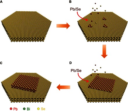
(A) Bi2Se3 nanoplate was first grown in solution. (B) Controlled injection of Pb and Se precursor into the Bi2Se3 nanoplate dispersion initiates the nucleation of PbSe on the nanoplate. (C) Final PbSe/Bi2Se3 heterostructure is produced after the reaction reaches the equilibrium in 3 hours. (D) The deposition of PbSe on Bi2Se3 nanoplate continues as the reaction proceeds.
The powder x-ray diffraction (PXRD) pattern of the as-synthesized sample can be indexed as two crystal phases, including the rhombohedral Bi2Se3 [Rm; Joint Committee on Powder Diffraction Standard (JCPDS) card no. 00-033-0214] and cubic PbSe (Fmm; JCPDS card no. 03-065-0300) (fig. S1). The morphology and structure of the as-synthesized heterostructure were further characterized with transmission electron microscopy (TEM). Figure 2A presents a typical TEM image of the heterostructure in which the PbSe layer partially covers the surface of the Bi2Se3 nanoplate. The boundary between the pure Bi2Se3 and PbSe/Bi2Se3 regions was labeled with a blue dashed line. A uniform moiré pattern with an approximate hexagonal symmetry is clearly observed in the area with the deposition of the PbSe layer on Bi2Se3 (Fig. 2, A and B). The high-resolution TEM (HRTEM) image shows clearly resolved lattice fringes that are dominated by the hexagonal Bi2Se3 crystal lattice (Fig. 2B). In contrast, no similar pattern was observed in the area without PbSe (fig. S2, A and B). The moiré pattern was also identified in the scanning TEM (STEM) image (figs. S3 and S4).
Fig. 2. TEM study of the PbSe/Bi2Se3 heterostructure.
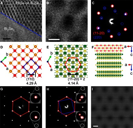
(A) Top-view TEM analysis of the interface of the PbSe/Bi2Se3 and pristine Bi2Se3 region as indicated by a blue dashed line. Scale bar, 20 nm. (B) HRTEM image of the PbSe/Bi2Se3 region. Scale bar, 5 nm. (C) SAED taken from the area in (B) with the guiding label to feature the symmetry of the diffraction spots. (D) Atomic crystal structure of the (001) plane in PbSe with a blue square to display the symmetry. (E) Atomic crystal structure of the (0001) plane in Bi2Se3 with a red hexagon to display the symmetry (sixfold, instead of threefold, is used to simplify the visualization). (F) Side view of the heterostructure with the relative orientation indicated by the electron diffraction. (G) Electron diffraction pattern of the pristine Bi2Se3 region. Insets are the zoom-in images on two separate diffraction spots. (H) Electron diffraction pattern of the PbSe/Bi2Se3 region. Insets are the zoom-in images on two separate diffraction spots, both showing a doublet split. (I) Simulated moiré pattern based on a pristine Bi2Se3 and expanded Bi2Se3 (0001) plane that exhibits the same symmetry and periodicity as those observed in (A) and (B). Scale bar, 5 nm.
The selected-area electron diffraction (SAED) patterns unraveled the relative crystallographic orientation of the PbSe layer and Bi2Se3 crystals in the heterostructure. SAED patterns on the region with moiré pattern (Fig. 2B) give two sets of diffraction spots with a hexagonal and a square symmetry, respectively (Fig. 2C). Each diffraction spot in the hexagonal pattern corresponds to the (11-20) family plane of the Bi2Se3 nanoplate (fig. S2C), and each diffraction spot in the square pattern can be indexed to the (110) family plane of the cubic PbSe layer. On the basis of the electron diffraction analysis, the crystal structure of PbSe and Bi2Se3 as well as the relative orientation are illustrated in Fig. 2 (D and E). Again, the single Bi2Se3 quintuple layer is considered as sixfold symmetric rather than threefold for simplification. The [11-20] direction of Bi2Se3 aligned well with the [110] direction of PbSe with essentially overlapping diffraction spots, suggesting an epitaxial relationship. The interplane distances of PbSe (110) and Bi2Se3 (11-20) planes are 4.29 and 4.14 Å, respectively, which are close enough (3.5% mismatch) for the epitaxial growth to occur. Therefore, the PbSe layer that deposited on the Bi2Se3 nanoplates with (001)/(0001) plane paralleled to each other and [110]/[11-20] axis aligned (Fig. 2F) was unequivocally determined.
DISCUSSION
Typical moiré patterns observed in TEM image originated from the mismatch between two distinct periodic lattices (38–42). However, overlapping the (001) plane of PbSe with the (0001) plane of Bi2Se3 could not produce the sixfold symmetric moiré pattern observed in our experiments (Fig. 2A). As a result, an additional lattice needs to be present in the heterostructure to produce the sixfold moiré pattern. The higher-order diffraction spots for Bi2Se3 on the heterostructure suggest the existence of an expanded Bi2Se3 lattice besides the pristine one. In the higher-order diffraction spots, each of the hexagonal spots splits into two (Fig. 2H). The brighter diffraction spots match well with the (11-20) lattice spacing of pristine Bi2Se3 crystal (Fig. 2G). In contrast, the weaker spots indicate an expanded Bi2Se3 lattice by about 3.5% (from 4.14 to 4.29 Å). The spacing of the enlarged Bi2Se3 (11-20) plane, 4.29 Å, coincides with the lattice spacing of (110) planes in PbSe crystal. Consequently, the expansion in the Bi2Se3 layers is attributed to the lattice constant mismatch in the [110] direction along which PbSe and Bi2Se3 crystals align with each other. The Bi2Se3 layers at the interface are thus expanded to accommodate the larger PbSe lattice.
The deformation of the existing lattice in underlying substrate, instead of the incoming epitaxial layers, to ensure a lattice match is distinct from most of the conventional epitaxy. Here, the layered nature and weak van der Waals interlayer interaction play a key role in the special expansion of the atomic layer on the underlying Bi2Se3 substrate and make it a unique soft template. Between each quintuple layer in the Bi2Se3 crystal, only the weak van der Waals force is present to hold the crystal together, which is considered to be much weaker than the typical chemical bonds. During the expansion or contraction of one layer of atoms, the adjacent quintuple layers are not strongly coupled to match the deformation that is typical in conventional epitaxy (25). The soft nature of the 2D Bi2Se3 crystal renders the opportunity that only the first interface layer of the atomic crystals expands (fig. S5) to accommodate the larger PbSe lattice, whereas the rest of the layers remain intact. Compared with the deformation of the 3D PbSe crystal, the expansion of 2D Bi2Se3 layers at the interface introduces weaker overall strain in the heterostructure, which is thermodynamically preferred. Furthermore, the elastic constants of deformation within the (001) plane of Bi2Se3 and PbSe are 103.2 and 120.8 GPa (43, 44), respectively. Therefore, in the perspective of stiffness, Bi2Se3 is more likely to deform compared with PbSe under the same strain that exists at the interface. To confirm the proposed atomic model, we simulated the moiré pattern by combining the pristine (0001) plane of Bi2Se3 (4.14 Å) with an expanded lattice (4.29 Å) (fig. S5). Expectedly, the resulted moiré pattern exhibits a sixfold symmetry (Fig. 2I) that is highly consistent with the experimentally observed moiré pattern in our heterostructure (Fig. 2, A and B).
We have further conducted the cross-sectional TEM (Fig. 3A) and STEM (Fig. 3B) studies to further confirm the atomic structure of the PbSe/Bi2Se3 epitaxial heterostructure. The composition line scan profile across the interface obtained shows that Pb and Bi contents are solely present in PbSe and Bi2Se3 regions, respectively, whereas Se exists in both materials (Fig. 3C). Because Se density in Bi2Se3 (2.47 g/cm3) is higher than that in PbSe (2.24 g/cm3), the Se amount increases slightly from PbSe to Bi2Se3 crystal. 2D mapping of Pb, Bi, and Se element (Fig. 3D) further provides an explicit distribution of each element. In both line scan profile and elemental mapping, the HRTEM of the interface (Fig. 3E) indicates that both segments exhibit excellent crystallinity with an atomically sharp interface. The clear fringe in the PbSe showed a period of 0.31 nm, as expected for the fcc PbSe (001) plane. The line scan profile and elemental mapping of Bi and Pb show a gradual transition across the interface, which might be due to the resolution of the STEM image. Together, the cross-sectional TEM studies further confirm the epitaxial growth of highly crystalline PbSe layer on top of the Bi2Se3 nanoplate, as illustrated by the schematic in Fig. 3F.
Fig. 3. Electron diffraction and moiré pattern analysis of the PbSe/Bi2Se3 heterostructure.
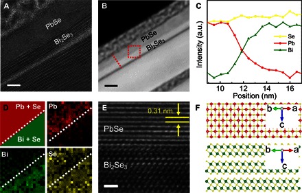
(A) Cross-sectional TEM image of the PbSe/Bi2Se3 heterostructure prepared by focused ion beam (FIB). A polycrystalline Pt layer was deposited on top of the nanoplate for sample preparation. Scale bar, 5 nm. (B) Cross-sectional high-angle annular dark-field STEM (HAADF-STEM) image of the PbSe/Bi2Se3 heterostructure. Scale bar, 10 nm. (C) Composition line scan profile across the interface [along the dashed red line in (B)] obtained by the energy-dispersive x-ray spectroscopy integrated with HAADF-STEM (HAADF-STEM-EDS), with normalized intensity. a.u., arbitrary units. (D) Elemental mapping of Pb, Bi, and Se in the region indicated by the red square in (B). (E) Cross-sectional HRTEM analysis of the interface. Scale bar, 1 nm. (F) Schematic illustration on the atomic structure of the PbSe/Bi2Se3 corresponding to the perspective in (E).
The symmetry-mismatched epitaxy observed in the PbSe/Bi2Se3 system is a special crystal growth in solution-phase synthesized nanocrystals (36). The atoms in the (001) plane of the fcc PbSe crystal exhibit a square symmetry, whereas the (0001) plane of the rhombohedral Bi2Se3 has a trigonal/hexagonal lattice (for single atomic layer). Here, we discuss the symmetry of individual atomic layer instead of the 3D crystal. To date, most of the epitaxial growth reported in the solution phase rigidly follow the rule of lattice symmetry matching requirement, including the typical cases of fourfold fcc Pd (100)//fcc Pt (100) (45), sixfold fcc Pt (111)//hexagonal MoS2 (001) (46), and sixfold wurtzite CdS (001)//wurtzite CdSe (001) (47). The alike symmetry between the crystals or the specific growth planes is mandatory to saturate the dangling bonds that are present at the interface. However, the dangling bond–free surface in the 2D atomic crystals promises a totally new possibility of epitaxial growth. The cleavage of the 2D layered compounds, such as Bi2Se3 and MoS2, could create a clean surface that is free of unsaturated atoms. The weak van der Waals force applies a weaker regulation than the unsaturated chemical atoms on the surface of typical crystalline layer, as demonstrated by several successful epitaxial growths with large lattice misfit (up to >50%) (22, 24, 25, 28, 35). In this case, the layered Bi2Se3 nanoplate guides the growth of the PbSe layer but does not require an exactly conformal lattice with one-to-one bond matching. The soft nature of the layered Bi2Se3 allows the deformation of the atomic layers near the interface without causing severe distortion of the entire nanoplates. The interface Bi2Se3 layers expand to match the larger PbSe lattice (by 3.5%) and ensure the energy minimum epitaxial growth that could not be realized in the traditional rigid substrates. Accordingly, the layered crystals that are held together by the loose van der Waals force are demonstrated to function as the unique soft substrate for the epitaxial growth of highly dissimilar materials. The discovery of the new epitaxy mode would open up new possibilities to enable the atomic-scale integration of materials with highly disparate crystal structures and functions.
Considering the similar sixfold symmetry of (0001) surface of the underlying Bi2Se3 and (111) surface of the cubic PbSe, a symmetry-matched epitaxial relationship of PbSe (111)//Bi2Se3 (0001) would have been a logical expectation instead of our observed symmetry-mismatched PbSe (001)//Bi2Se3 (0001). To better understand the unique symmetry-mismatched epitaxy, we have constructed a series of atomic models for PbSe/Bi2Se3 heterostructures and conducted DFT calculations to probe the interfacial bonding and energy. In particular, three types of PbSe planes, including (001), (011), and (111) were considered for epitaxial interfacing with the Bi2Se3 (0001) surface (Fig. 4), and the corresponding interfacial energy was calculated. Significantly, the DFT calculation indicates that PbSe (001)//Bi2Se3 (0001) is the most preferred epitaxial relation with the lowest interfacial energy of 0.031 eV/Å2, followed by interfacial energy of 0.046 eV/Å2 in PbSe (111)//Bi2Se3 (0001) and then 0.056 eV/Å2 in PbSe (011)//Bi2Se3 (0001) (Fig. 4). In addition, the smallest equilibrium atom distances in PbSe (001)//Bi2Se3 (0001) and PbSe (011)//Bi2Se3 (0001) are 3.30 and 3.27 Å, respectively, comparable to the typical Pb–Se bond distance, suggesting the effective bond formation between PbSe (001) and (011) plane with Bi2Se3 (0001) plane. It is worth noting that the interfacial Pb–Se distance (3.30 Å) is smaller than the distance of selenium atoms between two van der Waals layers (3.49 Å), indicating that the top Bi2Se3 layer has a strong coupling to the epitaxial PbSe layer. In contrast, the smallest equilibrium atom distance in the PbSe (111)//Bi2Se3 (0001) interface is 3.59 Å, which is too large for effective bond formation. Therefore, no chemical bond is expected to be present in this model, further confirming that the PbSe (111)//Bi2Se3 (0001) epitaxial relationship is unfavorable, in spite of a similar sixfold symmetry (Fig. 4C). Another factor that influences the epitaxy selectivity is the dangling bond density at the interface. On the basis of the simulated bonding configuration (Fig. 4), the dangling bond densities for PbSe (001), (011), and (111) surfaces on the Bi2Se3 (0001) surface are 0.093/Å2, 0.113/Å2, and 0.185/Å2, respectively. PbSe (001) exhibits the lowest dangling bond density, further suggesting that PbSe (001)//Bi2Se3 (0001) is the preferred epitaxial relationship. Considering all the above factors, the PbSe (111)//Bi2Se3 (0001) model exhibits the largest number of nonbonded electrons, which induces a great lability in the structure. In contrast, the PbSe (001)//Bi2Se3 (0001) model shows improved stability with fewer dangling bonds. Together, the DFT calculation results support our interpretation of the experimentally observed epitaxial relationship in the PbSe/Bi2Se3 heterostructure.
Fig. 4. DFT calculation of heterostructure models with various orientations.
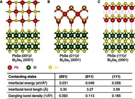
(A to C) Atomic structure with Bi2Se3 (0001) parallel to PbSe (001) (A), (011) (B), and (111) (C) after energy relaxation. Table shows the interfacial energy, bond length, and dangling bond density for each type of interface.
The formation of the heterointerface in the nearly perfect epitaxial heterostructures could suppress the thermal transport while largely retaining the electronic properties, which is desirable for thermoelectric applications. In particular, previous studies have shown that the lamellar nanostructures or superlattices could enable significant thermal conductivity reduction and thermoelectric enhancement (48–50). The assembled PbSe/Bi2Se3 heterostructures exhibit superlattice-like structure in the local region and therefore may offer unique opportunities in thermoelectric devices. To explore the thermoelectric properties of the high-quality PbSe/Bi2Se3 heterostructures, we processed the nanostructured powders into bulk pellet using hot pressing to enable thermoelectric property measurement. At room temperature, both the values of electrical conductivity and Seebeck coefficient of PbSe/Bi2Se3 heterostructure are lower than those of the pristine Bi2Se3 nanoplate, which leads to a smaller power factor (Fig. 5, A to C). Notably, with increasing temperature, the power factor of PbSe/Bi2Se3 rises rapidly and becomes about 70% higher than that of pristine Bi2Se3 at 575 K because of the simultaneous increase in both electrical conductivity and Seebeck coefficient (Fig. 5C). The most interesting property of the heterostructure is the extremely low thermal conductivity within the measured temperature range (Fig. 5, D and E). At the temperature between 298 and 575 K, the thermal conductivity of the PbSe/Bi2Se3 pellet ranges from 0.30 to 0.29 W/m·K, which is considerably lower than that of the Bi2Se3 nanoplate pellet (0.57 to 0.50 W/m·K) and PbSe (0.9 to 1.4 W/m·K) (51, 52). The efficient phonon scattering at the PbSe and Bi2Se3 heterointerface is considered to be mainly responsible for such a low thermal conductivity (49, 53–55), which is similar to the mechanism in PbTe and Bi2Te3 nanowire heterostructure (56). On the basis of the measured electrical conductivities, Seebeck coefficients, and thermal conductivities, we have calculated the temperature-dependent thermoelectric figure of merit (ZT = S2σT/κ) of both nanostructured pellets (Fig. 5F). Significantly, the PbSe/Bi2Se3 heterostructures exhibit considerably higher ZT value than the pure Bi2Se3 with a three-time enhancement at 575 K, which can be largely attributed to the ultralow thermal conductivity and increased Seebeck coefficient of the epitaxial heterostructures. Together, the PbSe/Bi2Se3 epitaxial heterostructure could successfully suppress the thermal transport without seriously sacrificing the electrical conductivity via enhanced phonon scattering and increase the Seebeck coefficient, thus leading to significantly improved thermoelectric performance.
Fig. 5. Thermoelectric performance of pristine Bi2Se3 nanoplate and the heterostructure.
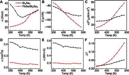
(A to F) The electrical conductivity σ (A), Seebeck coefficient S (B), power factor σS2 (C), thermal diffusivity α (D), thermal conductivity κ (E), and figure of merit ZT (F) of pristine Bi2Se3 nanoplate and PbSe/Bi2Se3 heterostructure bulk, which were prepared by hot pressing under the same conditions.
In summary, we have reported an example of symmetry-mismatched epitaxial growth of the PbSe (001) plane on the 2D Bi2Se3 nanoplate (0001) plane in the solution phase. The dangling bond–free (0001) plane of Bi2Se3 exerts a weak regulation on the growth of the PbSe layer because of the absence of one-to-one atomic chemical bond formation and results in a unique soft template for epitaxy. The DFT calculations suggest the lower interfacial energy in the PbSe (001)//Bi2Se3 (0001) model than in the PbSe (011)//Bi2Se3 (0001) or PbSe (111)//Bi2Se3 (0001) model and thus a more thermodynamically stable structure. Our study on the symmetry-mismatched epitaxial growth in liquid-phase nanomaterials enriches the toolbox for the fabrication of high-quality heterostructures via the epitaxy method and opens up new possibilities in engineering the interface within composite materials to enable high-performance electronic, optoelectronic, and thermoelectric devices. In particular, the growth of PbSe/Bi2Se3 heterostructures or superlattices could effectively reduce the thermal conductivity by the interface scattering of phonon and therefore provides a scalable approach to bulk quantities of epitaxial nanostructures with precisely engineered thermoelectric properties.
MATERIALS AND METHODS
Synthesis of lead selenide/bismuth selenide heterostructure
For the bismuth selenide nanoplates, 0.2 mmol of Bi(NO3)3⋅5H2O (0.0970 g), 0.3 mmol of NaSeO3 (0.0519 g), and 2 mmol of polyvinylpyrrolidone (0.2223 g) were dissolved in 10 ml of ethylene glycol (EG). The mixture was stirred for 10 min and then heated to 190°C (in about 12 min) in a 25-ml three-neck flask equipped with a thermal couple and a reflux condenser in a heating mantle. After 3 hours, the temperature was decreased to 180°C and allowed to stabilize for 20 min. One milliliter of 0.1 M Pb(CH3COO)2⋅3H2O and 1 ml of 0.1 M Na2SeO3 both in EG solution were simultaneously injected into the flask using a dual syringe pump with a rate of 250 μl/min. After the temperature was maintained at 180°C for 3hours, the heating mantle was removed and the mixture was allowed to cool down to room temperature naturally. The mixture was then centrifuged at 12,000 rpm for 10 min after the addition of 30 ml of isopropanol. The supernatant was discarded, and the solid was dispersed in another 40 ml of isopropanol. The solid was washed with isopropanol and centrifuged three times before the final product was dispersed in isopropanol for further characterization.
DFT modeling
The Vienna Ab initio Simulation Package (VASP) with the projector-augmented wave method using the Perdew-Becke-Ernzerhof generalized gradient approximation for the exchange-correlation functional was used to perform structural optimization and electronic structure calculation. A plane-wave basis with a cutoff energy of 450 eV and Γ-centered k-point meshes of constant density was used to fully relax both bulk and slab structures with an energy convergence threshold of 10−5 eV and residual forces of less than 10−2 eV/Å. For example, Γ-centered k-point meshes of 16 × 16 × 1 were used for a single quintuple layer of Bi2Se3.
Thermoelectric measurement
To characterize the thermoelectric properties in out-of-plane direction, disc [12.7 mm (D) × 2 mm (H)] and cylinder [4 mm (D) × 10 mm (H)] specimens were separately prepared for thermal conductivity and power factor measurement. For disc specimens, the dried powders were ground and loaded into a graphite die with an inner diameter of 12.7 mm (for cylinder samples, the inner diameter of the die was 4 mm) in the glove box under an argon atmosphere with an oxygen level below 3.5 parts per million. Then, the graphite die with loaded powder was removed from the glove box and immediately sintered by dc-induced hot pressing at 663 K for 15 min at a force of 1.4 metric tons (for cylinder samples, the force is ~0.1 metric ton to ensure a similar pressure). The hot-pressed discs had a thickness of about 2 mm, and the cylinder specimens had a length of around 10 mm.
The hot-pressed discs were used for out-of-plane thermal conductivity characterizations, whereas the cylinder specimens were used directly for the measurement of out-of-plane electrical properties. The electrical conductivity of the samples was measured by a four-point dc switching technique, and the Seebeck coefficient was measured by a static dc method on the basis of the slope of the voltage versus temperature difference curves using the commercial equipment (ZEM-3, ULVAC Riko) under helium atmosphere. The out-of-plane thermal conductivity was measured on the disc specimens. Thermal conductivity κ = dDCp was calculated using the measured density (d) by Archimedean method, specific heat (Cp) by differential scanning calorimetry (DSC 404 C, Netzsch), and thermal diffusivity (D) by the laser flash method (LAF 447 Nanoflash, Netzsch). The errors of measurement for electrical resistivity, Seebeck coefficient, and thermal conductivity were ±5, ±5, and ±7%, respectively. Here, all the reported values were measured and compared in out-of-plane direction of Bi2Se3 and PbSe/Bi2Se3 samples.
Characterization
Characterizations were carried out using HRTEM, SAED, HAADF-STEM-EDS (TEM, T12 Quick CryoEM, and CryoET FEI; acceleration voltage, 120 kV; Titan S/TEM FEI; acceleration voltage, 300 kV), and PXRD (PANalytical X'Pert Pro x-ray powder diffractometer). The cross-sectional sample was prepared by covering the film sample on the SiO2/Si substrate with a layer of polycrystalline Pt and then cleaving with FIB.
Supplementary Material
Acknowledgments
Funding: X.D. acknowledges the partial financial support by NSF DMR1508144. Y.H. acknowledges the financial support by NSF EFRI-1433541. Y.X. and V.O. acknowledge financial support from the U.S. Department of Energy (DOE) under grant DE-FG02-07ER46433 and use of resources of the National Energy Research Scientific Computing Center, a DOE Office of Science user facility supported by the U.S. DOE Office of Science under contract no. DE-AC02-05CH11231. N.K. acknowledges financial support from U.S. DOE Nuclear Energy University Program fellowship support. Author contributions: X.D. designed the research. Z.L. synthesized the PbSe/Bi2Se3 heterostructure and conducted all the structural analysis as well as the design of schematic. Z.L., A.Y., and C.-Y.C. solved the SAED and HRTEM images for heterostructure. A.Y., Q.H., and Y.W. assisted with the moiré pattern simulation and DFT calculations. Y.X. and V.O. performed the DFT calculations. N.K., Y.Z., J.M., and R.Z. prepared the bulk sample and performed thermoelectric measurement. X.D. and Z.L. co-wrote the paper. X.D. and Y.H. supervised the research. All authors discussed the results and commented on the manuscript. Competing interests: The authors declare that they have no competing interests. Data and materials availability: All data needed to evaluate the conclusions in the paper are present in the paper and/or the Supplementary Materials. Additional data related to this paper may be requested from the authors by emailing xduan@chem.ucla.edu.
SUPPLEMENTARY MATERIALS
Supplementary material for this article is available at http://advances.sciencemag.org/cgi/content/full/2/10/e1600993/DC1
fig. S1. PXRD pattern for the PbSe/Bi2Se3 heterostructure.
fig. S2. HRTEM analysis of the pure Bi2Se3 region in the PbSe/Bi2Se3 heterostructure.
fig. S3. Low-magnification representative STEM image of the PbSe/Bi2Se3 heterostructure.
fig. S4. High-magnification representative STEM image of the PbSe/Bi2Se3 heterostructure.
fig. S5. Atomic crystal structure for the intrinsic and expanded Bi2Se3 (0001) layers.
note S1. DFT modeling of PbSe (001)–Bi2Se3 (001), PbSe (011)–Bi2Se3 (0001), and PbSe (111)–Bi2Se3 (0001) interfaces.
REFERENCES AND NOTES
- 1.Lauhon L. J., Gudiksen M. S., Wang D., Lieber C. M., Epitaxial core–shell and core–multishell nanowire heterostructures. Nature 420, 57–61 (2002). [DOI] [PubMed] [Google Scholar]
- 2.Amano H., Sawaki N., Akasaki I., Toyoda Y., Metalorganic vapor phase epitaxial growth of a high-quality GaN film using an AlN buffer layer. Appl. Phys. Lett. 48, 353–355 (1986). [Google Scholar]
- 3.Chen O., Zhao J., Chauhan V. P., Cui J., Wong C., Harris D. K., Wei H., Han H.-S., Fukumura D., Jain R. K., Bawendi M. G., Compact high-quality CdSe–CdS core–shell nanocrystals with narrow emission linewidths and suppressed blinking. Nat. Mater. 12, 445–451 (2013). [DOI] [PMC free article] [PubMed] [Google Scholar]
- 4.Ma Y., Li W., Cho E. C., Li Z., Yu T., Zeng J., Xie Z., Xia Y., Au@Ag core–shell nanocubes with finely tuned and well-controlled sizes, shell thicknesses, and optical properties. ACS Nano 4, 6725–6734 (2010). [DOI] [PMC free article] [PubMed] [Google Scholar]
- 5.Lim B., Jiang M., Camargo P. H. C., Cho E. C., Tao J., Lu X., Zhu Y., Xia Y., Pd-Pt bimetallic nanodendrites with high activity for oxygen reduction. Science 324, 1302–1305 (2009). [DOI] [PubMed] [Google Scholar]
- 6.Lee H., Habas S. E., Somorjai G. A., Yang P., Localized Pd overgrowth on cubic Pt nanocrystals for enhanced electrocatalytic oxidation of formic acid. J. Am. Chem. Soc. 130, 5406–5407 (2008). [DOI] [PubMed] [Google Scholar]
- 7.Kolmakov A., Klenov D. O., Lilach Y., Stemmer S., Moskovits M., Enhanced gas sensing by individual SnO2 nanowires and nanobelts functionalized with Pd catalyst particles. Nano Lett. 5, 667–673 (2005). [DOI] [PubMed] [Google Scholar]
- 8.Diroll B. T., Murray C. B., High-temperature photoluminescence of CdSe/CdS core/shell nanoheterostructures. ACS Nano 8, 6466–6474 (2014). [DOI] [PubMed] [Google Scholar]
- 9.Stringfellow G. B., Epitaxy. Rep. Prog. Phys. 45, 469–525 (1982). [Google Scholar]
- 10.Amano H., Growth of GaN layers on sapphire by low-temperature-deposited buffer layers and realization of p-type GaN by magesium doping and electron beam irradiation (Nobel Lecture). Angew. Chem. Int. Ed. 54, 7764–7769 (2015). [DOI] [PubMed] [Google Scholar]
- 11.Gong Y., Lin J., Wang X., Shi G., Lei S., Lin Z., Zou X., Ye G., Vajtai R., Yakobson B. I., Terrones H., Terrones M., Tay B. K., Lou J., Pantelides S. T., Liu Z., Zhou W., Ajayan P. M., Vertical and in-plane heterostructures from WS2/MoS2 monolayers. Nat. Mater. 13, 1135–1142 (2014). [DOI] [PubMed] [Google Scholar]
- 12.Duan X., Wang C., Shaw J. C., Cheng R., Chen Y., Li H., Wu X., Tang Y., Zhang Q., Pan A., Jiang J., Yu R., Huang Y., Duan X., Lateral epitaxial growth of two-dimensional layered semiconductor heterojunctions. Nat. Nanotechnol. 9, 1024–1030 (2014). [DOI] [PMC free article] [PubMed] [Google Scholar]
- 13.Markov I., Stoyanov S., Mechanisms of epitaxial growth. Contemp. Phys. 28, 267–320 (1987). [Google Scholar]
- 14.Narayan J., Larson B. C., Domain epitaxy: A unified paradigm for thin film growth. J. Appl. Phys. 93, 278–285 (2003). [Google Scholar]
- 15.Zhang D.-F., Sun L.-D., Jia C.-J., Yan Z.-G., You L.-P., Yan C.-H., Hierarchical assembly of SnO2 nanorod arrays on α-Fe2O3 nanotubes: A case of interfacial lattice compatibility. J. Am. Chem. Soc. 127, 13492–13493 (2005). [DOI] [PubMed] [Google Scholar]
- 16.Grundmann M., Formation of epitaxial domains: Unified theory and survey of experimental results. Phys. Status Solidi B 248, 805–824 (2011). [Google Scholar]
- 17.Liu Y., Goebl J., Yin Y., Templated synthesis of nanostructured materials. Chem. Soc. Rev. 42, 2610–2653 (2013). [DOI] [PubMed] [Google Scholar]
- 18.Fan F.-R., Liu D.-Y., Wu Y.-F., Duan S., Xie Z.-X., Jiang Z.-Y., Tian Z.-Q., Epitaxial growth of heterogeneous metal nanocrystals: From gold nano-octahedra to palladium and silver nanocubes. J. Am. Chem. Soc. 130, 6949–6951 (2008). [DOI] [PubMed] [Google Scholar]
- 19.Jin M., Zhang H., Wang J., Zhong X., Lu N., Li Z., Xie Z., Kim M. J., Xia Y., Copper can still be epitaxially deposited on palladium nanocrystals to generate core–shell nanocubes despite their large lattice mismatch. ACS Nano 6, 2566–2573 (2012). [DOI] [PubMed] [Google Scholar]
- 20.Tsuji M., Yamaguchi D., Matsunaga M., Ikedo K., Epitaxial growth of Au@Ni core–shell nanocrystals prepared using a two-step reduction method. Cryst. Growth Des. 11, 1995–2005 (2011). [Google Scholar]
- 21.Tsuji M., Yamaguchi D., Matsunaga M., Alam M. J., Epitaxial growth of Au@Cu core–shell nanocrystals prepared using the PVP-assisted polyol reduction method. Cryst. Growth Des. 10, 5129–5135 (2010). [Google Scholar]
- 22.Shim G. W., Yoo K., Seo S.-B., Shin J., Jung D. Y., Kang I. S., Ahn C. W., Cho B. J., Choi S.-Y., Large-area single-layer MoSe2 and its van der Waals heterostructures. ACS Nano 8, 6655–6662 (2014). [DOI] [PubMed] [Google Scholar]
- 23.Geim A. K., Grigorieva I. V., Van der Waals heterostructures. Nature 499, 419–425 (2013). [DOI] [PubMed] [Google Scholar]
- 24.Shi Y., Zhou W., Lu A.-Y., Fang W., Lee Y.-H., Hsu A. L., Kim S. M., Kim K. K., Yang H. Y., Li L.-J., Idrobo J.-C., Kong J., Van der Waals epitaxy of MoS2 layers using graphene as growth templates. Nano Lett. 12, 2784–2791 (2012). [DOI] [PubMed] [Google Scholar]
- 25.Koma A., Van der Waals epitaxy—A new epitaxial growth method for a highly lattice-mismatched systems. Thin Solid Films 216, 72–76 (1992). [Google Scholar]
- 26.Zhang H., Ultrathin two-dimensional nanomaterials. ACS Nano 9, 9451–9469 (2015). [DOI] [PubMed] [Google Scholar]
- 27.Tan C., Zhang H., Epitaxial growth of hetero-nanostructures based on ultrathin two-dimensional nanosheets. J. Am. Chem. Soc. 137, 12162–12174 (2015). [DOI] [PubMed] [Google Scholar]
- 28.Ueno K., Saiki K., Shimada T., Koma A., Epitaxial growth of transition metal dichalcogenides on cleaved faces of mica. J. Vac. Sci. Technol. A 8, 68–72 (1990). [Google Scholar]
- 29.Palmstrom C. J., Epitaxy of dissimilar materials. Annu. Rev. Mater. Sci. 25, 389–415 (1995). [Google Scholar]
- 30.Fan Z., Zhu Y., Huang X., Han Y., Wang Q., Liu Q., Huang Y., Gan C. L., Zhang H., Synthesis of ultrathin face-centered-cubic Au@Pt and Au@Pd core–shell nanoplates from hexagonal-close-packed Au square sheets. Angew. Chem. Int. Ed. 54, 5672–5676 (2015). [DOI] [PubMed] [Google Scholar]
- 31.Fan Z., Zhang H., Crystal phase-controlled synthesis, properties and applications of noble metal nanomaterials. Chem. Soc. Rev. 45, 63–82 (2016). [DOI] [PubMed] [Google Scholar]
- 32.Fan Z., Bosman M., Huang X., Huang D., Yu Y., Ong K. P., Akimov Y. A., Wu L., Li B., Wu J., Huang Y., Liu Q., Png C. E., Gan C. L., Yang P., Zhang H., Stabilization of 4H hexagonal phase in gold nanoribbons. Nat. Commun. 6, 7684 (2015). [DOI] [PMC free article] [PubMed] [Google Scholar]
- 33.Fan Z., Huang X., Han Y., Bosman M., Wang Q., Zhu Y., Liu Q., Li B., Zeng Z., Wu J., Shi W., Li S., Gan C. L., Zhang H., Surface modification–induced phase transformation of hexagonal close–packed gold square sheets. Nat. Commun. 6, 6571 (2015). [DOI] [PubMed] [Google Scholar]
- 34.Johnson N. J. J., van Veggel F. C. J. M., Sodium lanthanide fluoride core–shell nanocrystals: A general perspective on epitaxial shell growth. Nano Res. 6, 547–561 (2013). [Google Scholar]
- 35.Utama M. I. B., Belarre F. J., Magen C., Peng B., Arbiol J., Xiong Q., Incommensurate van der Waals epitaxy of nanowire arrays: A case study with ZnO on muscovite mica substrates. Nano Lett. 12, 2146–2152 (2012). [DOI] [PubMed] [Google Scholar]
- 36.Zhu Y., Zhou Y., Utama M. I. B., de la Mata M., Zhao Y., Zhang Q., Peng B., Magen C., Arbiol J., Xiong Q., Solution phase van der Waals epitaxy of ZnO wire arrays. Nanoscale 5, 7242–7249 (2013). [DOI] [PubMed] [Google Scholar]
- 37.Lin Z., Chen Y., Yin A., He Q., Huang X., Xu Y., Liu Y., Zhong X., Huang Y., Duan X, Solution processable colloidal nanoplates as building blocks for high-performance electronic thin films on flexible substrates. Nano Lett. 14, 6547–6553 (2014). [DOI] [PubMed] [Google Scholar]
- 38.Kim J. H., Kim K., Lee Z., The hide-and-seek of grain boundaries from moiré pattern fringe of two-dimensional graphene. Sci. Rep. 5, 12508 (2015). [DOI] [PMC free article] [PubMed] [Google Scholar]
- 39.Gao Y., Zhang Y., Chen P., Li Y., Liu M., Gao T., Ma D., Chen Y., Cheng Z., Qiu X., Duan W., Liu Z., Toward single-layer uniform hexagonal boron nitride–graphene patchworks with zigzag linking edges. Nano Lett. 13, 3439–3443 (2013). [DOI] [PubMed] [Google Scholar]
- 40.Sutter P., Cortes R., Lahiri J., Sutter E., Interface formation in monolayer graphene-boron nitride heterostructures. Nano Lett. 12, 4869–4874 (2012). [DOI] [PubMed] [Google Scholar]
- 41.Gao L., Guest J. R., Guisinger N. P., Epitaxial graphene on Cu(111). Nano Lett. 10, 3512–3516 (2010). [DOI] [PubMed] [Google Scholar]
- 42.Reckinger N., Van Hooijdonk E., Joucken F., Tyurnina A. V., Lucas S., Colomer J.-F., Anomalous moiré pattern of graphene investigated by scanning tunneling microscopy: Evidence of graphene growth on oxidized Cu(111). Nano Res. 7, 154–162 (2014). [Google Scholar]
- 43.Gao X., Zhou M., Cheng Y., Ji G., First-principles study of structural, elastic, electronic and thermodynamic properties of topological insulator Bi2Se3 under pressure. Philos. Mag. 96, 208–222 (2016). [Google Scholar]
- 44.Lach-hab M., Papaconstantopoulos D. A., Mehl M. J., Electronic structure calculations of lead chalcogenides PbS, PbSe, PbTe. J. Phys. Chem. Solids 63, 833–841 (2002). [Google Scholar]
- 45.Habas S. E., Lee H., Radmilovic V., Somorjai G. A., Yang P., Shaping binary metal nanocrystals through epitaxial seeded growth. Nat. Mater. 6, 692–697 (2007). [DOI] [PubMed] [Google Scholar]
- 46.Huang X., Zeng Z., Bao S., Wang M., Qi X., Fan Z., Zhang H., Solution-phase epitaxial growth of noble metal nanostructures on dispersible single-layer molybdenum disulfide nanosheets. Nat. Commun. 4, 1444 (2013). [DOI] [PubMed] [Google Scholar]
- 47.Talapin D. V., Nelson J. H., Shevchenko E. V., Aloni S., Sadtler B., Alivisatos A. P., Seeded growth of highly luminescent CdSe/CdS nanoheterostructures with rod and tetrapod morphologies. Nano Lett. 7, 2951–2959 (2007). [DOI] [PubMed] [Google Scholar]
- 48.Girard S. N., Chasapis T. C., He J., Zhou X., Hatzikraniotis E., Uher C., Paraskevopoulos K. M., Dravid V. P., Kanatzidis M. G., PbTe-PbSnS2 thermoelectric composites: Low lattice thermal conductivity from large microstructures. Energy Environ. Sci. 5, 8716–8725 (2012). [Google Scholar]
- 49.Ikeda T., Collins L. A., Ravi V. A., Gascoin F. S., Haile S. M., Snyder G. J., Self-assembled nanometer lamellae of thermoelectric PbTe and Sb2Te3 with epitaxy-like interfaces. Chem. Mater. 19, 763–767 (2007). [Google Scholar]
- 50.Venkatasubramanian R., Siivola E., Colpitts T., O’Quinn B., Thin-film thermoelectric devices with high room-temperature figures of merit. Nature 413, 597–602 (2001). [DOI] [PubMed] [Google Scholar]
- 51.Heideman C. L., Tepfer S., Lin Q., Rostek R., Zschack P., Anderson M. D., Anderson I. M., Johnson D. C., Designed synthesis, structure, and properties of a family of ferecrystalline compounds [(PbSe)1.00]m(MoSe2)n. J. Am. Chem. Soc. 135, 11055–11062 (2013). [DOI] [PubMed] [Google Scholar]
- 52.Liang W., Rabin O., Hochbaum A. I., Fardy M., Zhang M., Yang P., Thermoelectric properties of p-type PbSe nanowires. Nano Res. 2, 394–399 (2009). [DOI] [PubMed] [Google Scholar]
- 53.Snyder G. J., Toberer E. S., Complex thermoelectric materials. Nat. Mater. 7, 105–114 (2008). [DOI] [PubMed] [Google Scholar]
- 54.Lo S.-H., He J., Biswas K., Kanatzidis M. G., Dravid V. P., Phonon scattering and thermal conductivity in p-type nanostructured PbTe-BaTe bulk thermoelectric materials. Adv. Funct. Mater. 22, 5175–5184 (2012). [Google Scholar]
- 55.Fang H., Bahk J.-H., Feng T., Cheng Z., Mohammed A. M. S., Wang X., Ruan X., Shakouri A., Wu Y., Thermoelectric properties of solution-synthesized n-type Bi2Te3 nanocomposites modulated by Se: An experimental and theoretical study. Nano Res. 9, 117–127 (2016). [Google Scholar]
- 56.Fang H., Feng T., Yang H., Ruan X., Wu Y., Synthesis and thermoelectric properties of compositional-modulated lead telluride–bismuth telluride nanowire heterostructures. Nano Lett. 13, 2058–2063 (2013). [DOI] [PubMed] [Google Scholar]
Associated Data
This section collects any data citations, data availability statements, or supplementary materials included in this article.
Supplementary Materials
Supplementary material for this article is available at http://advances.sciencemag.org/cgi/content/full/2/10/e1600993/DC1
fig. S1. PXRD pattern for the PbSe/Bi2Se3 heterostructure.
fig. S2. HRTEM analysis of the pure Bi2Se3 region in the PbSe/Bi2Se3 heterostructure.
fig. S3. Low-magnification representative STEM image of the PbSe/Bi2Se3 heterostructure.
fig. S4. High-magnification representative STEM image of the PbSe/Bi2Se3 heterostructure.
fig. S5. Atomic crystal structure for the intrinsic and expanded Bi2Se3 (0001) layers.
note S1. DFT modeling of PbSe (001)–Bi2Se3 (001), PbSe (011)–Bi2Se3 (0001), and PbSe (111)–Bi2Se3 (0001) interfaces.