Abstract
In this work, we demonstrate a novel carrier transporting combination made of tungsten trioxide (WO3) nanomaterials and Cs2CO3/PCBM buffer bilayer for the fabrication of perovskite solar cells (PSCs). Two different types of WO3, including nanoparticles and nanorods, were prepared by sol-gel process and hydrothermal method, respectively. Cs2CO3/PCBM buffer bilayer was inserted between WO3 and perovskite layers to improve charge transfer efficiency and formation of pinhole-free perovskite layer. Besides, the leakage current of the devices containing Cs2CO3/PCBM buffer bilayer was significantly suppressed. The optimized device based on WO3 nanoparticles and Cs2CO3/PCBM bilayer showed an open-circuit voltage of 0.84 V, a short-circuit current density of 20.40 mA/cm2, a fill factor of 0.61, and a power conversion efficiency of 10.49 %, which were significantly higher than those of PSCs without Cs2CO3/PCBM buffer bilayer. The results revealed that the combination of WO3 nanomaterials and Cs2CO3/PCBM bilayer provides an effective solution for improving performances of PSCs.
Keywords: Tungsten trioxide, Perovskite solar cells, Hydrothermal, Buffer bilayer
Background
Perovskite solar cells (PSCs) have made impressive progress during several years due to high power conversion efficiency (PCE), low cost, and large-scale fabrication. The PCE values of PSCs have sharply risen from 3.8 to 21.1 % owing to excellent optical and electronic properties of organic/inorganic halide perovskite materials [1, 2], such as high absorption coefficient, long exciton diffusion length, and tunable band gap. The most used perovskite material is methylammonium lead iodide (CH3NH3PbI3 or MAPbI3) that is made of methylammonium iodide (MAI) and lead iodide (PbI2) [3]. Despite those advantages of PSCs, there still exist many challenges to commercialize PSC technologies in the near future, e.g., easy degradation from MAPbI3 to the starting material PbI2 under water and oxygen exposure, hysteresis under forward and reverse scans [4], and the usage of lead that is not friendly to our living environment.
The device architecture of PSCs is constructed with the configuration of fluorine-doped tin oxide (FTO)/electron transporting layer (ETL)/perovskite/hole transporting layer (HTL)/metal electrode. Many n-type metal oxide materials, including zinc oxide (ZnO), titanium dioxide (TiO2), tin dioxide, and tungsten trioxide (WO3) [5–8], can be used as ETL in PSCs. On the other hand, p-type materials, such as vanadium oxide, nickel oxide, and molybdenum trioxide, can be utilized as HTL in PSCs [9–11]. Academic researches on TiO2 and ZnO-based ETLs for PSCs have been extensively reported in the literatures [12–15]. In fact, TiO2 exhibits relatively lower electrical conductivity among common inorganic electron transporting materials, implying lower transportation efficiency for carriers. High sintering temperature is also necessary for the preparation of high-quality TiO2 layers, which is unfavorable for low-cost manufacturing. The low-temperature process for the formation of TiO2 layer would limit its conductivity and electron transporting ability. On the other hand, ZnO possesses higher electron mobility and can be prepared via a simple fabrication process such as the hydrothermal method. However, there are still some drawbacks for ZnO to serve as ETL in PSCs. It is reported that ZnO could react with weak acids or bases [16], and its optoelectrical properties as well as surface morphology would be consequently affected. Furthermore, the perovskite may decompose to PbI2 upon thermal annealing on ZnO surface due to the reaction between released OH− ions from ZnO and the component CH3NH3I. This usually results in the collapse of the perovskite structure and leads to poor device performance and stability of ZnO-based PSCs [17]. In addition to TiO2 and ZnO, WO3 is regarded as a potential candidate for the construction of PSCs. WO3 is an n-type material with electron mobility of 10–20 cm2/V s that is in the middle of TiO2 and ZnO [16, 18]. The optical band gap of WO3 ranges from 2.7 to 3.2 eV depending on different crystalline structures [19]. Furthermore, WO3 has high transmission in the visible region and excellent chemical stability which is better than that of ZnO [20]. After surveying previous literatures, we notice that electron transporting WO3 is less reported in the area of PSCs. In 2013, Amassian’s group firstly used untreated WO3 nanorods to fabricate PSCs with the highest PCE of 3.9 % [8]. The efficiency of PSC was promoted to 9.1 % by using TiCl4-treated WO3 nanorods as the ETL. In 2015, Ma et al. adopted the low-temperature amorphous WOX as electron selective layer for PSCs with CH3NH3PbIXCl3-X as the absorber [16]. The WOX layer with a large quantity of nanocaves was used and the obtained PCE was 8.99 %. From a scientific and industrial viewpoint, developing alternatives or new types of materials is an essential issue to expand the diversity of research instead of adopting limited materials.
In this paper, we demonstrate the solution-processed WO3 nanoparticles layer (NL) and nanorod arrays (NAs) as the ETL for PSCs. To further improve the device performance of PSCs, ultra-thin cesium carbonate (Cs2CO3) and [6,6]-phenyl-C60 butyric acid methyl ester (PCBM) buffer layers were deposited on the above WO3 layers. Cs2CO3 is an inorganic compound that is commonly used as the electron injection material in organic light-emitting diodes and organic solar cells [21–23], or as a surface modification material for transparent conducting oxide [24]. PCBM is an electron acceptor that is usually blended with poly(3-hexylthiophene-2,5-diyl) (P3HT) or other low-band-gap conjugated polymers to fabricate bulk heterojunction solar cells [25, 26]. Based on the above discussion, we propose the new PSC structure with the configuration of FTO/WO3 NL or NAs/Cs2CO3/PCBM/MAPbI3/P3HT/Au which is illustrated in Fig. 1a. In this device architecture, P3HT acts as the HTL to collect holes from MAPbI3 layer, while WO3 covered with Cs2CO3/PCBM buffer bilayer is used to collect electrons. The energy level diagram of the whole device is illustrated in Fig. 1b. The lowest unoccupied molecular orbital of PCBM lies between the conduction band of WO3 and perovskite layers that is favored for electron extraction from the perovskite layer; the existence of PCBM layer can also prohibit carrier recombination at interfaces and back electron transfer from WO3 to perovskite layers. The ultra-thin Cs2CO3 layer is incorporated between WO3 and PCBM layers to increase electron transfer across neighboring layers. Electrons can transport from PCBM to WO3 through the Cs2CO3 layer under the tunneling effect due to its ultra-thin thickness [27]. Besides, this Cs2CO3 layer can also act as the blocking layer to prevent carrier recombination at the interface between WO3 and PCBM layers. On the other hand, hole transport from perovskite to P3HT is undisturbed, as shown in Fig. 1b. The optical, morphological, and crystallinity investigations of the two types of WO3 were carried out by miscellaneous techniques, including transmission spectroscopy, scanning electron microscopy (SEM), atomic force microscopy (AFM), and X-ray diffraction (XRD) analysis. The SEM and AFM images as well as photoluminescence (PL) quenching of the perovskite layer on pristine WO3 and WO3/Cs2CO3/PCBM layers were also performed to realize the role of Cs2CO3/PCBM bilayer on WO3 NL or NAs. Finally, WO3 NL or NAs-based PSCs without and with Cs2CO3/PCBM bilayers were fabricated and evaluated.
Fig. 1.
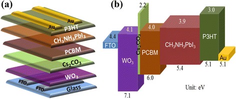
a Device structure and b energy level diagram of the PSCs
Methods
Characterization Methods
The UV-Vis absorption and transmission spectra of samples were measured by Princeton Instrument Acton 2150 spectrophotometer with a Xe lamp as a light source. The steady-state PL emission of the perovskite layer was measured using a He-Cd laser with double excitation wavelengths at 325/442 nm. The top-view and cross section SEM images of WO3 nanostructures and perovskite devices were obtained using JEOL 6700F FE-SEM. The surface morphology and roughness were obtained using a Bruker Innova AFM with tapping mode. The XRD patterns of samples were obtained using an X'Pert3 Powder X-ray Diffractometer, PANalytical Inc. with Cu-Kα radiation. The external quantum efficiency (EQE) measurement was conducted using a PV Measurements QEX10 instrument. The current density-voltage (J-V) curves of perovskite devices were performed using a Keithley 2400 digital sourcemeter under the sunlight simulator (Xenon Short Arc Lamp, USHIO UXL-10S) with irradiation intensity of 100 mW/cm2. The perovskite devices were masked with a metal aperture to define the active area of 4 mm2.
Preparation of WO3 NL
A solution of tungsten acid (H2WO4, 0.375 g) was dissolved in 6 mL of 30 wt% hydrogen peroxide aqueous solution and heated at 140 °C. After the solution was concentrated from 6 to 1 mL, 9 mL of de-ionized water was added into the above solution and treated with ultra-sonication for 1 h, followed by filtration with 0.45 μm PTFE filter to form the precursor solution. The WO3 NL was spin-cast on the FTO substrate at 2000 rpm for 30 s and heated at 200 °C for 10 min. A second spin-coating step was carried out, and the film was sintered at 450 °C for 30 min to form the final WO3 NL with thickness of about 50 nm, as verified by AFM step height measurement.
Preparation of WO3 NAs
WO3 NAs were prepared via the hydrothermal method. Sodium tungstate dihydrate (Na2WO4·2H2O, 4.125 g) was dissolved in 12.5 mL of de-ionized water and stirred at room temperature for 1 h. Into the above solution, 0.2 M hydrochloric acid aqueous solution was then added dropwise until the pH value of the solution was adjusted from 9.2 to 2.4. Afterward, de-ionized water was added till the total volume of the solution is 125 mL, followed by ultrasonic treatment for 30 min to form the precursor solution. A bath solution containing 20 mL of the precursor solution and 0.3 g of sodium chloride was poured into a teflon-lined autoclave. The WO3 NL on the FTO substrate was immersed with the surface downwards in the bath solution, and the autoclave was placed in a preheated oven at 170 °C for 120 min. The substrates were then taken out and cleaned with de-ionized water, acetone, and isopropyl alcohol (IPA) sequentially, followed by calcination at 500 °C for 1 h. The height of the obtained WO3 NAs is 300 nm, as verified by a SEM cross section.
Fabrication of Perovskite Solar Cells
The FTO conductive substrates were sequentially cleaned with detergent, de-ionized water, acetone, and IPA with ultra-sonication for 30 min, dried at 100 °C for 10 min to remove the solvent residue, and followed by UV-ozone treatment for 20 min. WO3 NL or NAs were prepared on the pre-cleaned FTO substrates according to the processes in the previous section. A solution of Cs2CO3 in de-ionized water (2 mg/mL) was dropped on the WO3 layer (NL or NAs); after waiting for 30 s, the substrate was spin-coated at 2500 rpm for 60 s, followed by heating treatment at 300 °C for 30 min in ambient environment. After cooling to room temperature, a solution of PCBM in chlorobenzene (20 mg/mL) was dropped on the Cs2CO3 layer; after waiting for 5 s, the substrate was spin-coated at 3000 rpm for 30 s, followed by heating treatment at 120 °C for 10 min in a vacuum oven. The perovskite layer CH3NH3PbI3 was formed via the two-step sequential deposition procedure. First, a PbI2 solution in DMF (462 mg/mL) was spin-coated on the WO3 layer at 5000 rpm for 30 s, and the substrate was placed in a petridish for 10 min, followed by heating treatment at 100 °C for 20 min in a vacuum oven. Second, a MAI solution in IPA (40 mg/mL) was dropped on the PbI2 layer; after waiting for 60 s, it was then spun at 5000 rpm for 30 s. The substrate was then heated at 100 °C for 20 min in a vacuum oven. The P3HT layer was formed by spin-coating from its solution in chlorobenzene (20 mg/mL) and heated at 100 °C for 30 min. Finally, gold electrodes were thermal-evaporated on the P3HT layer under a base pressure ~10−6 torr.
Results and Discussion
Nanostructural, Electrical, and Optical Analyses of Materials
Figure 2a, b show the top-view and cross section SEM images of WO3 NL, respectively. It is clearly seen that most WO3 nanoparticles are tightly formed with diameters ranging from 50 to 100 nm, while the thickness of WO3 NL is estimated to be 80–100 nm. Compared to some flat layers, this kind of WO3 NLs provides a larger surface area that is beneficial for carrier extraction and photovoltaic performance [28]. Some pinholes and aggregates are also observed on the surface, which can be further reduced by covering with adequate buffer layers such as Cs2CO3/PCBM bilayer to prevent trapping of electrons and direct contact of FTO and perovskite layer. Figure 2c shows the topographic image of WO3 NL deposited on the quartz substrate by AFM. The particle size and surface morphology of WO3 nanoparticles are consistent with those observed from SEM images. The surface roughness (R a) is calculated to be about 5.0 nm, indicative of a smooth surface of WO3 NL. The top-view and cross section SEM images of WO3 NAs are shown in Fig. 3c, b, respectively. Well-aligned WO3 NAs with length of about 300 nm are vertically grown on the WO3 NL. The total surface areas of WO3 NAs are supposed to be larger than the NL due to the high aspect ratio of nanorods, which might show a positive effect on carrier extraction and transportation. The surface morphology of WO3 NAs investigated by AFM technique is shown in Fig. 3c. Rod-like shapes and a higher R a value of 32 nm are observed for the prepared WO3 NAs in this study. To further compare the conductivity of WO3 NL and NAs, simple electron-only devices with the configuration of FTO/WO3/Au and FTO/WO3/Cs2CO3/Au were fabricated; the current-voltage characteristics of four devices were measured and shown in Fig. 4. It is seen that WO3 NAs show higher electrical conductivity and lower resistance compared to the WO3 NL. The results suggest that NAs-type of WO3 is more favorable for electron transport than the NL one. Furthermore, the electron current of the device FTO/WO3/Cs2CO3/Au is even higher than that without the Cs2CO3 layer, indicating an enhanced electron-extraction ability of this ETL system. According to the previous literatures [23, 29], a thin layer of Cs2CO3 is capable of lowering the work function of the underlying layer. In this study, the thin Cs2CO3 layer lowers the work function of the WO3 layer and thereby increases electron-extraction ability in this combined WO3/Cs2CO3 system. Figure 5a, b show the top-view SEM images of perovskite films deposited on the WO3 NL and NAs, respectively. There are many pinholes to be observed on the perovskite films, indicating higher probability of electron trapping and less light absorption in both cases. A similar observation has been reported in the previous literature [16], stating hole-forming and poor coverage of perovskite on the WO3 layer. To solve this problem, a thin Cs2CO3/PCBM bilayer is proposed to be inserted between WO3 and perovskite layers in this study. After depositing the Cs2CO3/PCBM bilayer, the R a values of WO3 NL and NAs were reduced to 0.874 and 30 nm, respectively, which is beneficial for the deposition of perovskite layer. From Fig. 5c, d, a pinhole-free perovskite surface with larger grain size was obtained on both WO3 layers covered with a Cs2CO3/PCBM bilayer, revealing higher surface coverage of the perovskite layer. Till now several techniques have been proposed to form a pinhole-free perovskite layer, such as solvent annealing [30], moisture-control method [31], inverted thermal annealing [32], addition of methylammonium bromide precursor [33], and the selection of lead sources [34]. Here we demonstrate an alternative way to reduce pinholes on perovskite layer by the incorporation of a Cs2CO3/PCBM bilayer. Besides, we notice that the perovskite with a larger grain size of 250–650 nm was formed on WO3 NL; on the contrary, the perovskite with smaller crystallites of 200–400 nm was found on WO3 NAs. It is concluded that the formation of perovskite layer is strongly influenced by the type of WO3 layer. Furthermore, some WO3 nanorods are observed to penetrate through the perovskite layer to the top surface, as shown in Fig. 5b. This would lead to direct contact of WO3 NAs and hole transporting P3HT layer and result in leakage current to lower photovoltaic properties of devices. The phenomenon of nanorod penetration can be largely suppressed by the incorporation of a Cs2CO3/PCBM bilayer on WO3 NAs, as revealed in Fig. 5d. The penetration of WO3 nanorods may be further suppressed by increasing the thickness of the perovskite layer; however, the carrier transport and diffusion length would also be affected that is unfavorable for device performance. In order to comprehend morphologies and roughness change for the deposition of Cs2CO3/PCBM bilayer on WO3 NL, the AFM images and R a values of the bare FTO, FTO/WO3 NL, and FTO/WO3 NL/Cs2CO3/PCBM were investigated and shown in Fig. 6. The polycrystalline feature of FTO surface in Fig. 6a, d is clearly changed to nanoparticle-aggregated morphology after depositing WO3 NL on top of FTO shown in Fig. 6b, e, and corresponding R a value is decreased from 23.8 to 18.9 nm, indicating that FTO surface is covered and smoothed by WO3 NL. Moreover, amorphous surface morphology and eliminated grain boundary are obtained for FTO/WO3 NL/Cs2CO3/PCBM with the smallest R a value of 4.79 nm, as shown in Fig. 6c, f. In other words, the surface properties of WO3 NL are further modified by the coverage of Cs2CO3/PCBM bilayer. The very smooth top surface is particularly suitable for the deposition of highly dense and pinhole-free perovskite layers.
Fig. 2.
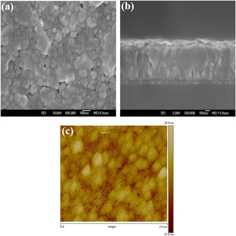
a Top-view, b cross section SEM, and c AFM topographic images of WO3 NL
Fig. 3.
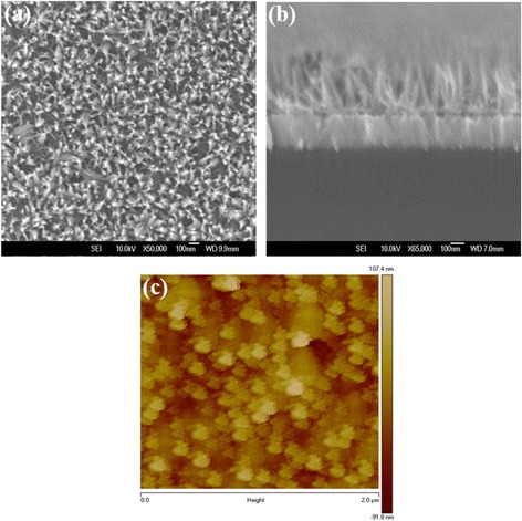
a Top-view, b cross section SEM, and c AFM topographic images of WO3 NAs
Fig. 4.
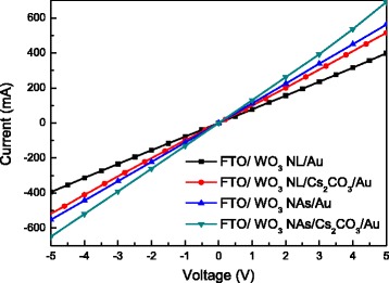
Linear sweep voltammetry curves of the four electron-only devices
Fig. 5.
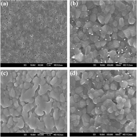
Top-view SEM images of the perovskite layers deposited a WO3 NL, b WO3 NAs, c WO3 NL/Cs2CO3/PCBM, and d WO3 NAs/Cs2CO3/PCBM
Fig. 6.
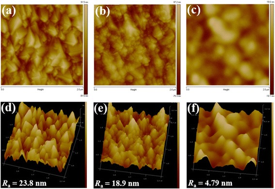
AFM topographic and 3D images of a, d bare FTO, b, e FTO/WO3 NL, and c, f FTO/WO3 NL/Cs2CO3/PCBM. The corresponding R a values of different films are also included
The XRD patterns of WO3 NL and NAs are shown in Fig. 7a. All diffraction peaks are well indexed to the standard diffraction pattern of hexagonal phase of WO3 (JCPDS 00-033-1387). Besides, these diffraction peaks are sharp and strong, indicating high-degree crystallization of the prepared WO3 samples in this research. The two main diffraction peaks located at 2θ = 23.4° and 29.3° are assigned to (001) and (200) planes, respectively, which is in good accordance with the previous report [35]. The XRD result suggests that the WO3 NAs are grown along (001) direction and aligned with the c-axis [36], not parallel to the FTO substrate. The crystalline phases of WO3 NL and NAs are concluded to be similar because of the same 2θ position of diffraction peaks in Fig. 7a. Furthermore, the intensities of diffraction peaks of WO3 NAs is stronger than those of WO3 NL, revealing a higher degree of crystallinty of WO3 NAs. Figure 7b shows the XRD patterns of perovskite film deposited on WO3 NL without and with a Cs2CO3/PCBM bilayer. First, three main diffraction peaks of perovskite film at 2θ = 14.1°, 28.5°, and 32.6° are assigned to (110), (220), and (310) planes, respectively, which are identical to the previous literature [37]. The rest of the weaker diffraction peaks located at 2θ = 24.5°, 40.5°, and 43.1° are assigned to (202), (224), and (314) planes, respectively. Second, those 2θ positions of diffraction peaks were unchanged after the incorporation of Cs2CO3/PCBM bilayer, indicating that the crystalline phase of perovskite was preserved. Third, the intensities of XRD patterns of perovskite on WO3 NL/Cs2CO3/PCBM are increased compared to those on untreated WO3 NL, revealing that the degree of crystallinity of perovskite is enhanced. The increased diffraction intensity can be realized by better crystallization of perovskite on a flatter WO3 NL/Cs2CO3/PCBM surface, which has been identified by AFM observation. The strengthened crystallization of perovskite can also be verified by SEM images in Fig. 6, exhibiting much larger perovskite crystals on Cs2CO3/PCBM-modified WO3 layer. This is the first report on the improvement of perovskite crystallization by incorporating Cs2CO3/PCBM bilayer on metal oxide layers. Besides, a small diffraction peak located at 2θ = 12.6° was found and assigned to the starting material PbI2, implying that the precursors were not compeletely transformed to perovskite structure. The existence of residual PbI2 is generally thought to be harmful to device performance, since carriers might be trapped and light absorption could be affected [38]. On the contrary, some research groups declare that the presence of a small amount of PbI2 can slightly enhance the device performance and suppress the carrier recombination [39–41]. It seems that the effect of residual PbI2 in PSCs is sometimes controversial.
Fig. 7.
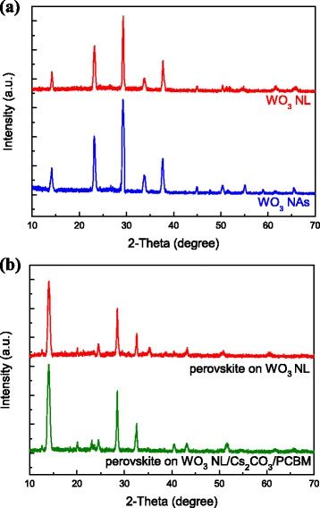
XRD patterns of a WO3 NL and NAs. b perovskite deposited on WO3 NL without and with Cs2CO3/PCBM bilayer
The transmission spectra of WO3 layer (NL and NAs) without and with Cs2CO3/PCBM bilayer are shown in Fig. 8a. The WO3 NL possesses the highest transmittance up to 80–95 % that is higher than WO3 NAs and FTO substrate in the visible region. This is beneficial for incident photons to enter devices and to be absorbed by the active layer. After the insertion of Cs2CO3/PCBM bilayer, the transmittance is decreased for both WO3 NL and NAs, which is due to the absorption nature of PCBM in the region from 300 to 500 nm. The absorption spectra of the perovskite layer on WO3 NL without and with Cs2CO3/PCBM bilayer are shown in Fig. 8b. The main absorption of the perovskite on WO3 NL with Cs2CO3/PCBM bilayer grows stronger in the range of 350 and 550 nm compared with that on the untreated WO3 NL. This is because a highly dense and pinhole-free perovskite layer is formed on Cs2CO3/PCBM-modified WO3 NL, which can absorb more incident light. More excitons are expected to generate inside the perovskite layer under sunlight exposure, and higher device efficiency would be achieved. It is also noted that the absorption edge of the perovskite is found around 770 nm that is similar on both untreated and Cs2CO3/PCBM-modified WO3 NLs. The steady-state PL spectra of the perovskite layer on the bare FTO substrate, WO3 NL, and WO3 NL/Cs2CO3/PCBM are shown in Fig. 8c. The max PL emission of the perovskite is located at 770 nm under excitation of a He-Cd laser source, which is in accordance with the previous report [42]. Distinct PL quenching of the perovskite is found when depositing on WO3 NL, implying better charge carrier extraction across the interface between the perovskite and WO3 NL [43]. By depositing Cs2CO3/PCBM bilayer on WO3 NL, the PL emission of the perovskite is further prohibited, indicating more effective carrier extraction and reduced recombination. In other words, the incorporation of Cs2CO3/PCBM bilayer facilitates carrier transfer from the perovskite layer to WO3 NL, which will help to improve short-circuit current density (J SC) and performance of PSCs. Similar behaviors including enhanced absorption and PL quenching of the perovskite layer can also be observed when incorporating Cs2CO3/PCBM bilayer on WO3 NAs.
Fig. 8.
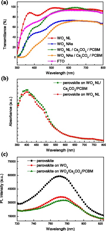
a Transmission spectra of different WO3 without and with Cs2CO3/PCBM bilayer. b Absorption spectra of the perovskite on WO3 NL without and with Cs2CO3/PCBM bilayer. c PL spectra of the perovskite on FTO, WO3 NL, and WO3 NL/Cs2CO3/PCBM
Photovoltaic Properties of Perovskite Devices
To evaluate photovoltaic performance of PSCs, five different device configurations were designed and are listed as follows:
Device A: FTO/WO3 NL/MAPbI3/P3HT/Au
Device B: FTO/WO3 NL/Cs2CO3/PCBM/MAPbI3/P3HT/Au
Device C: FTO/WO3 NAs/MAPbI3/P3HT/Au
Device D: FTO/WO3 NAs/Cs2CO3/PCBM/MAPbI3/P3HT/Au
Device E: FTO/MAPbI3/P3HT/Au
The J-V curves of all PSCs measured in the dark are shown in Fig. 9. The dark currents arose at 0.6 and 0.75 V for the devices based on untreated WO3 NAs and WO3 NL, respectively. After the insertion of Cs2CO3/PCBM bilayer, the dark currents arose at 0.7 and 0.85 V for the devices based on WO3 NAs and WO3 NL, respectively. The retardation in dark current brought by Cs2CO3/PCBM bilayer can be observed for both WO3 NL and NAs-based PSCs; moreover, the dark current of the device based on WO3 NL was more prohibited than that based on WO3 NAs. This could be due to the penetration of WO3 nanorods through the perovskite layer which was confirmed by SEM observation in Fig. 5b, d. The retardation in dark current means less leakage current and prohibition of back flow of electrons from WO3 to perovskite layer [44]. The suppression of leakage current can be realized by the passivation effect, i.e., the surface defects of WO3 layer were passivated by the incorporation of Cs2CO3/PCBM bilayer. Besides, a better energy level alignment was achieved by the insertion of Cs2CO3/PCBM bilayer shown in Fig. 1b, indicative of forming an ohmic contact from the FTO to perovskite layer for electron transport. Fewer electrons can be trapped and recombination rate is consequently decreased, leading to better device performance such as J SC and fill factor (FF). By comparison, the dark current of the reference device E without WO3 ETL arose around 0.4 V, implying the highest recombination rate of carriers among all devices.
Fig. 9.
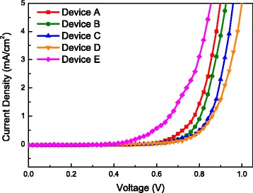
J-V curves of devices A through E in the dark
The J-V curves of the five devices A, B, C, D, and E under 100 mW/cm2 of sunlight irradiation are depicted in Fig. 10a, and the photovoltaic properties of all devices are summarized in Table 1. Device A showed an open-circuit voltage (V OC), J SC, FF, and PCE values of 0.78 V, 19.45 mA/cm2, 0.53, and 8.13 %, respectively, which were much higher than the previous report based on the same device configuration and perovskite material [8]. By introducing Cs2CO3/PCBM bilayer, the device B reached the highest PCE of 10.49 % that can be attributed to the improvement of J SC (20.40 mA/cm2) and FF (0.61) compared with device A. The J SC improvement can be realized from several experimental observations, including increased absorption in the visible range, enlarged grain size of perovskite crystals from SEM and AFM observation, and suppression of carrier recombination from PL quenching and dark current measurements. The explanations to the FF improvement include pinhole-free surface, reduced roughness of WO3 layer, prohibited leakage current, and lower recombination rate. The performance of the reference device E without WO3 was also evaluated and listed in Table 1. The poor device performance of device E indicates the necessity of WO3 ETL in the proposed PSC structure. To verify conversion efficiency versus wavelength and integrated photocurrent under light irradiation, the best device B was taken as an example and investigated. The EQE spectrum and integrated current density of device B are shown in Fig. 10b, revealing a quite stable EQE around 80 % from 400 to 700 nm. An integrated current density of 19.1 mA/cm2 is obtained, which is in good agreement with measured J SC under the sunlight simulator. Turning to devices C and D based on WO3 NAs, the device performance was also enhanced by the insertion of Cs2CO3/PCBM bilayer. Besides, we notice that the J SC and PCE of the devices based on WO3 NAs are not as high as those using WO3 NL as ETL, though WO3 NAs are characterized to own higher conductivity. The reasons to this phenomenon could be due to poorer surface coverage of perovskite layer on WO3 NAs and 20 % lower transmittance of WO3 NAs in the visible region; less incident photons would enter devices and be absorbed by perovskite layer, resulting in lower charge collection and J SC. Moreover, direct contact between ETL (WO3 NAs) and HTL (P3HT layer) from penetration of WO3 nanorods through perovskite layer leads to higher leakage current and lower FF. To examine the reproducibility of WO3-based PSCs without and with Cs2CO3/PCBM bilayer, PCE of 12 individual devices for devices A through E were measured and collected, and the statistical distributions of those devices are depicted in Fig. 10c. The averaged PCE values of devices A, B, C, D, and E are 7.96 ± 0.17, 10.10 ± 0.39, 5.63 ± 0.16, 7.50 ± 0.21, 2.80 ± 0.37, respectively, which are also listed in Table 1. It is clearly seen that a high level of reproducibility and reliability of PCE for each kind of device is obtained, and effective improvement in PCE can be deduced with the incorporation of Cs2CO3/PCBM bilayer on WO3-based PSCs.
Fig. 10.
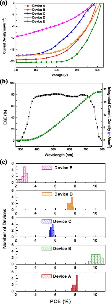
a J-V curves of devices without and with Cs2CO3/PCBM bilayer. b EQE spectrum and integrated current density of the best device B. c The histogram of the PCE values of 12 devices for devices A through E
Table 1.
Photovoltaic properties of the four PSCs with different configurations
| Devices | V OC (V) | J SC (mA/cm2) | FF | PCE (%) | Avg. PCE (%)a |
|---|---|---|---|---|---|
| A | 0.78 | 19.45 | 0.53 | 8.13 | 7.96 ± 0.17 |
| B | 0.84 | 20.40 | 0.61 | 10.49 | 10.10 ± 0.39 |
| C | 0.78 | 17.90 | 0.41 | 5.79 | 5.63 ± 0.16 |
| D | 0.82 | 18.20 | 0.52 | 7.71 | 7.50 ± 0.21 |
| E | 0.76 | 11.54 | 0.36 | 3.17 | 2.80 ± 0.37 |
aAverage PCE data are obtained from 12 devices
Conclusions
We demonstrated the insertion of Cs2CO3/PCBM bilayer between WO3 and perovskite layers to enhance the performance of PSCs. By inserting Cs2CO3/PCBM bilayer, the morphologies and roughness of WO3 were modified for better deposition of highly dense and pinhole-free perovskite layers. The degree of crystallinity of the perovskite as well as its absorption from 350 to 550 nm was also increased due to the incorporation of a Cs2CO3/PCBM bilayer. Besides, the prohibited PL emission of the perovskite brought by the Cs2CO3/PCBM bilayer indicates more effective carrier extraction and reduced recombination, which facilitates the carrier transfer from perovskite to WO3 layers. An optimized PCE of 10.49 % and a high J SC value of 20.40 mA/cm2 were achieved with the device based on WO3 NL covered with Cs2CO3/PCBM bilayer. Lower PCE of 7.71 % and J SC of 18.2 mA/cm2 of the device based on WO3 NAs were obtained due to the penetration of WO3 nanorods through the perovskite layer, larger surface roughness, and lower transmission of WO3 NAs compared with WO3 NL.
Acknowledgements
The authors gratefully thank the Ministry of Science and Technology of the Republic of China (MOST 105-2221-E-009-151) for the financial support of this work.
Funding
This work was supported by the Ministry of Science and Technology of the Republic of China under Contract No. MOST 105-2221-E-009-151.
Authors’ Contributions
CMC proposed the research idea, performed the experiments, and drafted the manuscript. ZKL and WJH participated in the sample preparation. SHY contributed to the data interpretation and manuscript writing and supervised the research. All authors read and approved the final manuscript.
Competing Interests
The authors declare that they have no competing interests.
Ethics Approval and Consent to Participate
Not applicable.
Abbreviations
- AFM
Atomic force microscopy
- EQE
External quantum efficiency
- ETL
Electron transporting layer
- FF
Fill factor
- HTL
Hole transporting layer
- JSC
Short-circuit current density
- J-V
Current density-voltage
- MAI
Methylammonium iodide
- MAPbI3
Methylammonium lead iodide
- NAs
Nanorod arrays
- NL
Nanoparticles layer
- P3HT
Poly(3-hexylthiophene-2,5-diyl)
- PCBM
[6,6]-Phenyl-C60 butyric acid methyl ester
- PCE
Power conversion efficiency
- PL
Photoluminescence
- PSCs
Perovskite solar cells
- SEM
Scanning electron microscopy
- VOC
Open-circuit voltage
- XRD
X-ray diffraction
Contributor Information
Chih-Ming Chen, Email: rochets534916@yahoo.com.tw.
Zheng-Kun Lin, Email: kill820619@yahoo.com.tw.
Wei-Jie Huang, Email: dm610456@gmail.com.
Sheng-Hsiung Yang, Email: yangsh@mail.nctu.edu.tw.
References
- 1.Kojima A, Teshima K, Shirai Y, Miyasaka T. Organometal halide perovskites as visible-light sensitizers for photovoltaic cells. J Am Chem Soc. 2009;131:6050–6051. doi: 10.1021/ja809598r. [DOI] [PubMed] [Google Scholar]
- 2.Saliba M, Matsui T, Seo JY, Domanski K, Correa-Baena JP, Nazeeruddin MK, Zakeeruddin SM, Tress W, Abate A, Hagfeldt A, Grätzel M. Cesium-containing triple cation perovskite solar cells: improved stability, reproducibility and high efficiency. Energy Environ Sci. 2016;9:1989–1997. doi: 10.1039/C5EE03874J. [DOI] [PMC free article] [PubMed] [Google Scholar]
- 3.Song TB, Chen Q, Zhou H, Jiang C, Wang HH, Yang YM, Liu Y, You J, Yang Y. Perovskite solar cells: film formation and properties. J Mater Chem A. 2015;3:9032–9050. doi: 10.1039/C4TA05246C. [DOI] [Google Scholar]
- 4.Chen B, Yang M, Priya S, Zhu K. Origin of J−V hysteresis in perovskite solar cells. J Phys Chem Lett. 2016;7:905–917. doi: 10.1021/acs.jpclett.6b00215. [DOI] [PubMed] [Google Scholar]
- 5.Liu D, Kelly TL. Perovskite solar cells with a planar heterojunction structure prepared using room-temperature solution processing techniques. Nat Photonics. 2014;8:133–138. doi: 10.1038/nphoton.2013.342. [DOI] [Google Scholar]
- 6.Ke W, Fang G, Wang J, Qin P, Tao H, Lei H, Liu Q, Dai X, Zhao X. Perovskite solar cell with an efficient TiO2 compact film. ACS Appl Mater Interfaces. 2014;6:15959–15965. doi: 10.1021/am503728d. [DOI] [PubMed] [Google Scholar]
- 7.Song J, Zheng E, Bian J, Wang XF, Tian W, Sanehira Y, Miyasaka T. Low-temperature SnO2-based electron selective contact for efficient and stable perovskite solar cells. J Mater Chem A. 2015;3:10837–10844. doi: 10.1039/C5TA01207D. [DOI] [Google Scholar]
- 8.Mahmood K, Swain BS, Kirmani AR, Amassian A. Highly efficient perovskite solar cells based on a nanostructured WO3–TiO2 core–shell electron transporting material. J Mater Chem A. 2015;3:9051–9057. doi: 10.1039/C4TA04883K. [DOI] [Google Scholar]
- 9.Troughton J, Bryant D, Wojciechowski K, Carnie MJ, Snaith H, Worsley DA, Watson TM. Highly efficient, flexible, indium-free perovskite solar cells employing metallic substrates. J Mater Chem A. 2015;3:9141–9145. doi: 10.1039/C5TA01755F. [DOI] [Google Scholar]
- 10.Wang KC, Jeng JY, Shen PS, Chang YC, Diau EWG, Tsai CH, Chao TY, Hsu HC, Lin PY, Chen P, Guo TF, Wen TC. p-Type mesoscopic nickel oxide/organometallic perovskite heterojunction solar cells. Sci Rep. 2014;4:4756. doi: 10.1038/srep04756. [DOI] [PMC free article] [PubMed] [Google Scholar]
- 11.Hou F, Su Z, Jin F, Yan X, Wang L, Zhao H, Zhu J, Chu B, Li W. Efficient and stable planar heterojunction perovskite solar cells with an MoO3/PEDOT:PSS hole transporting layer. Nanoscale. 2015;7:9427–9432. doi: 10.1039/C5NR01864A. [DOI] [PubMed] [Google Scholar]
- 12.Yang D, Yang R, Zhang J, Yang Z, Liu S, Li C. High efficiency flexible perovskite solar cells using superior low temperature TiO2. Energy Environ Sci. 2015;8:3208–3214. doi: 10.1039/C5EE02155C. [DOI] [Google Scholar]
- 13.Giordano F, Abate A, Baena JPC, Saliba M, Matsui T, Im SH, Zakeeruddin SM, Nazeeruddin MK, Hagfeldt A, Gräetzel M. Enhanced electronic properties in mesoporous TiO2 via lithium doping for high-efficiency perovskite solar cells. Nat Commun. 2016;7:10379. doi: 10.1038/ncomms10379. [DOI] [PMC free article] [PubMed] [Google Scholar]
- 14.Xu X, Zhang H, Shi J, Dong J, Luo Y, Li D, Meng Q. Highly efficient planar perovskite solar cells with a TiO2/ZnO electron transport bilayer. J Mater Chem A. 2015;3:19288–19293. doi: 10.1039/C5TA04239A. [DOI] [Google Scholar]
- 15.Mahmood K, Swain BS, Amassian A. Double-layered ZnO nanostructures for efficient perovskite solar cells. Nanoscale. 2014;6:14674–14678. doi: 10.1039/C4NR04383A. [DOI] [PubMed] [Google Scholar]
- 16.Wang K, Shi Y, Dong Q, Li Y, Wang S, Yu X, Wu M, Ma T. Low-temperature and solution-processed amorphous WOX as electron-selective layer for perovskite solar cells. J Phys Chem Lett. 2015;6:755–759. doi: 10.1021/acs.jpclett.5b00010. [DOI] [PubMed] [Google Scholar]
- 17.Cheng Y, Yang QD, Xiao J, Xue Q, Li HW, Guan Z, Yip HL, Tsang SW. Decomposition of organometal halide perovskite films on zinc oxide nanoparticles. ACS Appl Mater Interfaces. 2015;7:19986–19993. doi: 10.1021/acsami.5b04695. [DOI] [PubMed] [Google Scholar]
- 18.Ramana CV, Utsunomiya S, Ewing RC, Julien CM, Becker U. Structural stability and phase transitions in WO3 thin films. J Phys Chem B. 2006;110:10430–10435. doi: 10.1021/jp056664i. [DOI] [PubMed] [Google Scholar]
- 19.Weinhardt L, Blum M, Bär M, Heske C, Cole B, Marsen B, Miller EL. Electronic surface level positions of WO3 thin films for photoelectrochemical hydrogen production. J Phys Chem C. 2008;112:3078–3082. doi: 10.1021/jp7100286. [DOI] [Google Scholar]
- 20.Szilágyi IM, Madarász J, Pokol G, Király P, Tárkányi G, Saukko S, Mizsei J, Tóth AL, Szabó A, Varga-Josepovits K. Stability and controlled composition of hexagonal WO3. Chem Mater. 2008;20:4116–4125. doi: 10.1021/cm800668x. [DOI] [Google Scholar]
- 21.Cho H, Choi JM, Yoo S. Highly transparent organic light-emitting diodes with a metallic top electrode: the dual role of a Cs2CO3 layer. Opt Express. 2011;19:1113–1121. doi: 10.1364/OE.19.001113. [DOI] [PubMed] [Google Scholar]
- 22.Liao HH, Chen LM, Xu Z, Li G, Yang Y. Highly efficient inverted polymer solar cell by low temperature annealing of Cs2CO3 Interlayer. Appl Phys Lett. 2008;92:173303. doi: 10.1063/1.2918983. [DOI] [Google Scholar]
- 23.Huang J, Xu Z, Yang Y. Low-work-function surface formed by solution-processed and thermally deposited nanoscale layers of cesium carbonate. Adv Funct Mater. 2007;17:1966–1973. doi: 10.1002/adfm.200700051. [DOI] [Google Scholar]
- 24.Hu Q, Wu J, Jiang C, Liu T, Que X, Zhu R, Gong Q. Engineering of electron-selective contact for perovskite solar cells with efficiency exceeding 15 % ACS Nano. 2014;8:10161–10167. doi: 10.1021/nn5029828. [DOI] [PubMed] [Google Scholar]
- 25.Chi D, Qu S, Wang Z, Wang J. High efficiency P3HT:PCBM solar cells with an inserted PCBM layer. J Mater Chem C. 2014;2:4383–4387. doi: 10.1039/c4tc00003j. [DOI] [Google Scholar]
- 26.Dang MT, Wantz G, Bejbouji H, Urien M, Dautel OJ, Vignau L, Hirsch L. Polymeric solar cells based on P3HT:PCBM: Role of the casting solvent. Sol Energy Mater Sol Cells. 2011;95:3408–3418. doi: 10.1016/j.solmat.2011.07.039. [DOI] [Google Scholar]
- 27.Zhang Y, Cui W, Zhu Y, Zu F, Liao L, Lee ST, Sun B. High efficiency hybrid PEDOT:PSS/nanostructured silicon Schottky junction solar cells by doping-free rear contact. Energy Environ Sci. 2015;8:297–302. doi: 10.1039/C4EE02282C. [DOI] [Google Scholar]
- 28.Yang Y, Ri K, Mei A, Liu L, Hu M, Liu T, Li X, Han H. The size effect of TiO2 nanoparticles on a printable mesoscopic perovskite solar cell. J Mater Chem A. 2015;3:9103–9107. doi: 10.1039/C4TA07030E. [DOI] [Google Scholar]
- 29.Cheng G, Tong WY, Low KH, Che CM. Thermal-annealing-free inverted polymer solar cells using ZnO/Cs2CO3 bilayer as electron-selective layer. Sol Energy Mater Sol Cells. 2012;103:164–170. doi: 10.1016/j.solmat.2012.04.022. [DOI] [Google Scholar]
- 30.Liu J, Gao C, He X, Ye Q, Ouyang L, Zhuang D, Liao C, Mei J, Lau W. Improved crystallization of perovskite films by optimized solvent annealing for high efficiency solar cell. ACS Appl Mater Interfaces. 2015;7:24008–24015. doi: 10.1021/acsami.5b06780. [DOI] [PubMed] [Google Scholar]
- 31.You J, Yang YM, Hong Z, Song TB, Meng L, Liu Y, Jiang C, Zhou H, Chang WH, Li G, Yang Y. Moisture assisted perovskite film growth for high performance solar cells. Appl Phys Lett. 2014;105:183902. doi: 10.1063/1.4901510. [DOI] [Google Scholar]
- 32.Dong G, Yang Y, Sheng L, Xia D, Su T, Fan R, Shi Y, Wang J. Inverted thermal annealing of perovskite films: a method for enhancing photovoltaic device efficiency. RSC Adv. 2016;6:44034–44040. doi: 10.1039/C6RA07497A. [DOI] [Google Scholar]
- 33.Zhao L, Luo D, Wu J, Hu Q, Zhang W, Chen K, Liu T, Liu Y, Zhang Y, Liu F, Russell TP, Snaith HJ, Zhu R, Gong Q. High-performance inverted planar heterojunction perovskite solar cells based on lead acetate precursor with efficiency exceeding 18 % Adv Funct Mater. 2016;26:3508–3514. doi: 10.1002/adfm.201601175. [DOI] [Google Scholar]
- 34.Zhang W, Saliba M, Moore DT, Pathak SK, Hörantner MT, Stergiopoulos T, Stranks SD, Eperon GE, Alexander-Webber JA, Abate A, Sadhanala A, Yao S, Chen Y, Friend RH, Estroff LA, Wiesner U, Snaith HJ. Ultrasmooth organic–inorganic perovskite thin-film formation and crystallization for efficient planar heterojunction solar cells. Nat Commun. 2015;6:6142. doi: 10.1038/ncomms7142. [DOI] [PubMed] [Google Scholar]
- 35.Wu CS. Hydrothermal fabrication of WO3 hierarchical architectures: structure, growth and response. Nanomater. 2015;5:1250–1255. doi: 10.3390/nano5031250. [DOI] [PMC free article] [PubMed] [Google Scholar]
- 36.Huang K, Pan Q, Yang F, Ni S, Wei X, He D. Controllable synthesis of hexagonalWO3 nanostructures and their application in lithium batteries. J Phys D Appl Phys. 2008;41:155417. doi: 10.1088/0022-3727/41/15/155417. [DOI] [Google Scholar]
- 37.Qiu J, Qiu Y, Yan K, Zhong M, Mu C, Yan H, Yang S. All-solid-state hybrid solar cells based on a new organometal halide perovskite sensitizer and one-dimensional TiO2 nanowire arrays. Nanoscale. 2013;5:3245–3248. doi: 10.1039/c3nr00218g. [DOI] [PubMed] [Google Scholar]
- 38.Jiang C, Lim SL, Goh WP, Wei FX, Zhang J. Improvement of CH3NH3PbI3 formation for efficient and better reproducible mesoscopic perovskite solar cells. ACS Appl Mater Interfaces. 2015;7:24726–24732. doi: 10.1021/acsami.5b07446. [DOI] [PubMed] [Google Scholar]
- 39.Cao DH, Stoumpos CC, Malliakas CD, Katz MJ, Farha OK, Hupp JT, Kanatzidis MG. Remnant PbI2, an unforeseen necessity in high-efficiency hybrid perovskite-based solar cells? APL Mater. 2014;2:091101. doi: 10.1063/1.4895038. [DOI] [Google Scholar]
- 40.Chen Q, Zhou H, Song TB, Luo S, Hong Z, Duan HS, Dou L, Liu Y, Yang Y. Controllable self-induced passivation of hybrid lead iodide perovskites toward high performance solar cells. Nano Lett. 2014;14:4158–4163. doi: 10.1021/nl501838y. [DOI] [PubMed] [Google Scholar]
- 41.Zhou Y, Yang M, Vasiliev AL, Garces HF, Zhao Y, Wang D, Pang S, Zhu K, Padture NP. Growth control of compact CH3NH3PbI3 thin films via enhanced solid-state precursor reaction for efficient planar perovskite solar cells. J Mater Chem A. 2015;3:9249–9256. doi: 10.1039/C4TA07036D. [DOI] [Google Scholar]
- 42.Choi H, Mai CK, Kim HB, Jeong J, Song S, Bazan GC, Kim JY, Heeger AJ. Conjugated polyelectrolyte hole transport layer for inverted-type perovskite solar cells. Nat Commun. 2015;6:7348. doi: 10.1038/ncomms8348. [DOI] [PMC free article] [PubMed] [Google Scholar]
- 43.Tvingstedt K, Malinkiewicz O, Baumann A, Deibel C, Snaith HJ, Dyakonov V, Bolink HJ. Radiative efficiency of lead iodide based perovskite solar cells. Sci Rep. 2014;4:6071. doi: 10.1038/srep06071. [DOI] [PMC free article] [PubMed] [Google Scholar]
- 44.Dong H, Guo X, Li W, Wang L. Cesium carbonate as a surface modification material for organic–inorganic hybrid perovskite solar cells with enhanced performance. RSC Adv. 2014;4:60131–60134. doi: 10.1039/C4RA08565E. [DOI] [Google Scholar]


