Abstract
The ability to direct and sort individual biological and non-biological particles into spatially addressable locations is fundamentally important to the emerging field of single cell biology. Towards this goal, we demonstrate a new class of magnetophoretic transistors, which can switch single magnetically labeled cells and magnetic beads between different paths in a microfluidic chamber. Compared with prior work on magnetophoretic transistors driven by a two-dimensional in-plane rotating field, the addition of a vertical magnetic field bias provides significant advantages in preventing the formation of particle clumps and in better replicating the operating principles of circuits in general. However, the three-dimensional driving field requires a complete redesign of the magnetic track geometry and switching electrodes. We have solved this problem by developing several types of transistor geometries which can switch particles between two different tracks by either presenting a local energy barrier or by repelling magnetic objects away from a given track, hereby denoted as “barrier” and “repulsion” transistors, respectively. For both types of transistors, we observe complete switching of magnetic objects with currents of ~40 mA, which is consistent over a range of particle sizes (8-15 μm). The switching efficiency was also tested at various magnetic field strengths (50-90 Oe) and driving frequencies (0.1-0.6 Hz); however, we again found that the device performance only weakly depended on these parameters. These findings support the use of these novel transistor geometries to form circuit architectures in which cells can be placed in defined locations and retrieved on demand.
Graphical Abstract
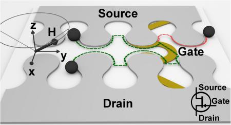
Magnetophoretic transistors switch magnetic particles and magnetically labeled cells between different paths in microfluidic channels in a tri-axial magnetic field.
Introduction
Biologists are increasingly turning to lab-on-a-chip systems to evaluate heterogeneous biological processes, which are difficult to analyze by traditional methods1-3. As such, the field of single cell analysis has emerged, where new platforms and assays enable the study of heterogeneous, and often rare, immunological and molecular mechanisms within single cells4,5. There has been significant interest in developing techniques for sorting and organizing single particles and cells in microfluidic chips based on various methods, such as sedimentation into micro-wells,6-8 encapsulation into droplets,9-10 capture by hydrodynamic traps,11-13 as well as active sorting based on electric fields,14-17 optical tweezers,18-19 acoustic pressure,20-21 and magnetic traps.22-24 Though these technologies have significant promise,25-27 many challenges must be surmounted to precisely organize the large number of single cells needed to analyze rare cellular events, which can be present at frequencies of 0.1% or less.
To overcome these barriers, we have developed a circuits-based approach to transport magnetic objects within microfluidic devices, which functions analogously to how electrons are moved inside computer chips. To achieve the highly scalable, automated, and programmable functionality of integrated circuits, it is necessary to develop the equivalent passive and active circuit elements, such as conductors, diodes, capacitors, and transistors, which can transport cells along desired paths inside microfluidic devices. Prior work on developing passive circuit elements has demonstrated that an external rotating field can move large ensembles of particles at controlled speeds along designated pathways (i.e., conductors).29 Active circuit elements have also been used to precisely control the motion of individual particles at specific junctions within the device (i.e., transistors).28 Though the operating principles of these switching junctions have been previously described,28-30 in brief, these devices are called “magnetophoretic transistors” because of their ability to replicate the properties of electronic transistors fabricated in solid state semiconductors. By analogy, these microfluidic devices are designed such that magnetic objects are unable to move across a gap when a gate electrode is OFF (non-conducting state). On the other hand, when a sufficiently large gate signal is applied, the magnetic objects can move across the gap with high efficiency (conducting state). By arranging these conductor and transistor elements into higher level system architectures, it is possible to organize arrays of single magnetic beads and magnetically labeled cells analogously to how a computer memory stores digital data.28,29 This manipulation strategy can also be generalized to non-magnetic particles by controlling the magnetic properties of the surrounding fluid.31-33
The first integrated magnetophoretic circuits were designed to operate in a two-dimensional (2-D) in-plane rotating magnetic field; however, these initial prototypes had an undesirable feature that impeded the system's performance. The problem arises from the fact that the particles experience strong attractive forces when exposed to an in-plane rotating magnetic field, which can lead to the formation of bead and cell aggregates.29 This problem leads to transport properties that are fundamentally different from electronic circuits, in which the mobile components (e.g. electrons) experience isotropic repulsion. For example, the self-limiting charging effect of a capacitor could not be achieved in a 2D rotating field, due to the lack of repulsion between the cells or beads.
To overcome this problem, we recently developed an alternative circuits-based approach for transporting magnetic objects, which instead used a three-dimensional (3-D) conical magnetic field (i.e., an in-plane rotating magnetic field superimposed with a static vertical field).34 The inclusion of the vertical field bias is advantageous because of inducing dipole-dipole repulsion between the magnetic objects, which not only reduces the tendency to form particle clumps but also allows for a better analogy between magnetophoretic circuits and their electronic counterparts. This improved analogy can impact the field of single cell analysis by establishing a self-limiting feature to control the number of objects in each array site. However, the use of the vertical field required a complete re-design of the magnetic track structure to achieve rectified particle transport.34
Our initial designs were based on ideas borrowed from the magnetic bubble literature,35-37 which used geometries, such as TI junctions, chevron patterns, and other structures to transport magnetic bubble domains inside iron garnet films. Though these geometries were capable of moving magnetic beads in fluids, we found that another design, i.e., the “drop-shape” pattern, was able to transport particles at higher frequencies and handle a wider range of particle sizes, and is, therefore, better suited for implementing the conductor elements.34 However, to date, we had not developed a transistor geometry that is compatible with the drop-shape conductor pattern when driven by a conical magnetic field.
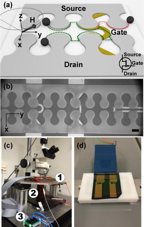
The goal of this paper is to demonstrate magnetophoretic transistor elements that are compatible with a conical driving field (i.e., in-plane rotating magnetic field combined with a vertical magnetic field bias). The basic operating principle of this transistor concept is illustrated in Fig. 1a-b. The system is composed of two magnetic tracks separated by a semiconducting gap. The gate electrode is established by an overlaid wire, which supplies a competing magnetic field and transforms the gap from a non-conducting to a conducting state. In the OFF mode, the particle stays on the same track with trajectories indicated by the red lines in Fig. 1a. In the ON mode, the particle moves to the adjacent track at the switching junction labeled “Gate” with trajectories as indicated by the green lines in Fig. 1a. We design and test a variety of transistor geometries (Fig. 1b shows a few examples) capable of switching the trajectory of magnetic beads and magnetically labeled single cells in a 3D conical magnetic field. The performance of a few transistor geometries is quantified as a function of the size and type of magnetic objects, as well as other operating parameters, such as the driving frequency, field strength, and cone angle (i.e., the angle between the total external field and the axis perpendicular to the chip surface). Interestingly, we find that the switching thresholds are fairly consistent over all tested conditions.
Figure 1. Magnetophoretic transistor and experimental setup.
Schematic of a sample transistor and particle trajectories when the transistor is operating in OFF mode (red dashed line) and ON mode (green dashed line) is illustrated in (a). Examples of fabricated transistors are shown in (b). Scale bar, 10 μm. The imaging station and magnetic field stage are shown in (c). The rotating field is produced by the coil (1), with another coil mounted underneath the platform (2). The rotating field and gate currents were controlled with a custom designed board (3). The chip is shown mounted in an IC test clip in (d).
Experimental Methods
The magnetic fields are produced by a customized apparatus fabricated in an iron plate machined into a four-pole structure, in which each of the arms is wrapped with 1000 turns of magnet wire (20 AWG). The magnetic field apparatus is powered by two programmable power supplies (Kepco BOP 20-5M, Flushing, NY), which are controlled by a high-precision, 8-channel voltage analog output board (DNR-AO-308, United Electronics Industries, Boston, MA) and operated with a customized LABVIEW program (National Instrument, Austin, TX). This analog output board is also used to supply up to 50mA currents to the gate electrodes. The magnetic fields are measured with a handheld Model 410 Gaussmeter Hall probe sensor (Lakeshore, Westerville, OH). In order to establish the static vertical field bias, another magnetic coil is placed underneath the stage (See Fig. 1c). As shown in Fig. 1d, we make electrical contact to the gate electrodes with an IC test clip (Ponoma Electronics, Everett, WA). The gate electrode currents are measured with a digital multimeter (Extech Ex430, Nashua, NH). A Retiga 2000R video camera mounted on a Leica DM LM microscope is used to record movies and obtain the bead and cell trajectories in a 20X objective. The trajectories are extracted from the experimental video data using a customized image recognition based in MATLAB (Mathworks, Natick, MA).
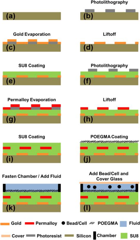
Though the detailed fabrication process is explained elsewhere,28 in brief, we fabricate aligned patterns of magnetic and metallic thin films on silicon wafers (University Wafer, Boston, MA) by conventional photolithographic liftoff process (Karl Suss MA6 mask aligner) using NFR16D2 negative photoresist. The metal layers are deposited by electron beam evaporation (Kurt Lesker, PVD 75), in which the metallic pattern consisted of a 5nm/100nm stack of Ti/Au, while the magnetic patterns consisted of a 100nm thick Ni80Fe20 film. The remaining photoresist is stripped with 1165 photoresist remover at 65°C. In between the metallic and magnetic layers, a 300nm thick conformal layer of SU8 photoresist is applied to achieve electrical insulation. This ultrathin SU8 layer is created by mixing SU8 3005 with cyclopentanone (Microchem, Westborough, MA) at a 5:2 ratio of SU8:cyclopentanone, which is spin-coated onto the chip at 3000 RPM. Another SU8 coating is applied on top of the chip in order to provide electrical insulation from the fluid and to establish a uniform surface chemistry for subsequent functionalization with a non-fouling polymer brush layer.
Poly(oligo(ethylene glycol) methyl ether methacrylate) (POEGMA) is grown directly on top of the top SU8 layer by surface-initiated atom transfer radical polymerization (SI-ATRP). Briefly, the SU8 top layer is first activated by generating hydroxyl groups on the surface as described elsewhere,38 followed by their conjugation to (3-aminopropyl)triethoxysilane (APTES). We then follow the process for growing the 30 nm thick POEGMA brush layer described elsewhere, in which an ATRP initiator is coupled to the amine groups installed on the surface of SU-8 by APTES coupling to SU-8, followed by SI-ATRP.39 A schematic of the fabrication procedure is shown in Figure 2.
Figure 2. Chip fabrication.
Starting from a cleaned silicon wafer (a), a photoresist is patterned (b), then a thin stack of Ti/Au is evaporated onto the entire surface (c), after which liftoff is performed (d), and finally a SU8 layer is applied to act as an insulator (e). These steps (b-e) are repeated with the magnetic permalloy layer (f-i). Finally, a POEGMA brush is grafted onto the SU8 top layer (j), followed by the installation of a 3D printed chamber and addition of DI water or PBS (k), and finally addition of cells or beads is followed by covering the chip with a coverslip to achieve a planar viewing window (l).
Three types of magnetic beads with mean diameters of 5.7 μm, 8.4 μm, and 15.6 μm are used in the transistor test experiments (CM-50-10, FCM-8056-2, and CM-150-10, respectively, from Spherotech, Lake Forest, IL). We also test the switching capability on human CD4+ T cells by magnetically labeling them with magnetic nanoparticles conjugated to anti-CD4 antibody (StemCell Technologies, Vancouver, Canada). The cell labeling process is performed using the protocols provided by the manufacturer, and cell isolation purity is confirmed by flow cytometry. Though we did not quantitatively measure the magnetic nanoparticle coverage on the cell membrane surface, the cells move reliably at driving frequencies below 0.3 Hz. Experiments on magnetic beads and cells are conducted in de-ionized (DI) water and phosphate-buffered saline (PBS), respectively. The cells and/or beads are suspended at a low concentration (~500 particles/μL) to reduce particle-particle interactions. A 10μL aliquot of bead solution is deposited on the chip and covered by a coverslip to create a microscopy-compatible viewing window. A 3D printer is used to fabricate the fluid holder, which is fastened to the chip with silicone glue.
Results
In our prior work, we numerically simulated the potential energy landscape of a magnetic point dipole above a drop-shape magnetic track pattern exposed to a conical time-varying magnetic field.34 We demonstrated that it is possible to achieve rectified particle transport along the track axis for a specific range of cone angles between 30° – 60°. The basic transport mechanism relies on symmetry breaking during two distinct intervals of motion, which correspond to the alternating sections of positive and negative curvature. The first interval of motion involves smooth translation of the particle around the section of positive (convex) curvature, which occurs when the external field has an in-plane component that is parallel to the outward normal of the substrate curvature. The second interval of motion involves a sudden jump between two curvature inflection points, which occurs when the in-plane field component is anti-parallel to the outward normal of the substrate curvature. For each complete cycle of the field rotation, the particle moves by one array period. Due to the linear relationship between the bead velocity and the driving frequency of the rotating field, the particle motion behaves analogously to Ohm's law for electrical circuits. Previous work has shown that both bi-directional and uni-directional motion can be achieved by adjusting the symmetry of the magnetic track shape.34 However, to date, no attempts have been made to implement the transistor functionality in a conical magnetic field.
Here, we consider a system in which two drop-shape magnetic track patterns are positioned in near proximity, and we test the ability of different micro-wire geometries (i.e., transistors) to switch magnetic particles between the two magnetic tracks. The goal of this work is to identify a few effective transistor geometries and analyze the switching thresholds as a function of experimental control parameters, including external field strength, cone angle, bead size, and frequency of the driving field. Our general strategy for designing the transistors is based on establishing magnetic field profiles that: 1) repel particles from the magnetic track by reducing the local magnetic field, or 2) attract particles towards the electrode by strengthening the particle's interaction with the external field. Though we have tested more than 50 transistor designs, we present only a few geometries that enable high-efficiency switching with the lowest possible currents, which can be broadly classified into these two general classes.
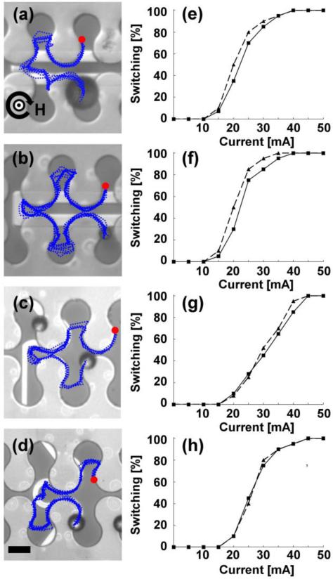
The first transistor class, which hereafter we denote as “barrier transistors” (see Figure 3), uses a small current loop to induce a local magnetic energy barrier when the particle reaches the transistor junction. As shown in the diagram of Fig. 1a, the switch point is the intersection of the magnetic track and the metal electrode, which hereafter we denote as the “gate”. When the gate is ON, the magnetic particle can switch between two adjacent tracks, hereafter denoted as a “successful switching event”. When a particle remains on the same track despite the presence of a gate signal, this is considered to be an unsuccessful switching event. For the barrier transistors, switching occurs only when the gate current within the loop produces a magnetic field that is parallel to the vertical component of the external field. The local energy minimum established by the current loop causes the particle to become momentarily trapped, after which the particle's location becomes out-of-phase with the traveling potential energy landscape of the first track. When the nearby energy minimum of the opposite track arrives at the junction, the particle then resumes its path along the second track, but in the opposite direction.
Figure 3. Barrier transistors.
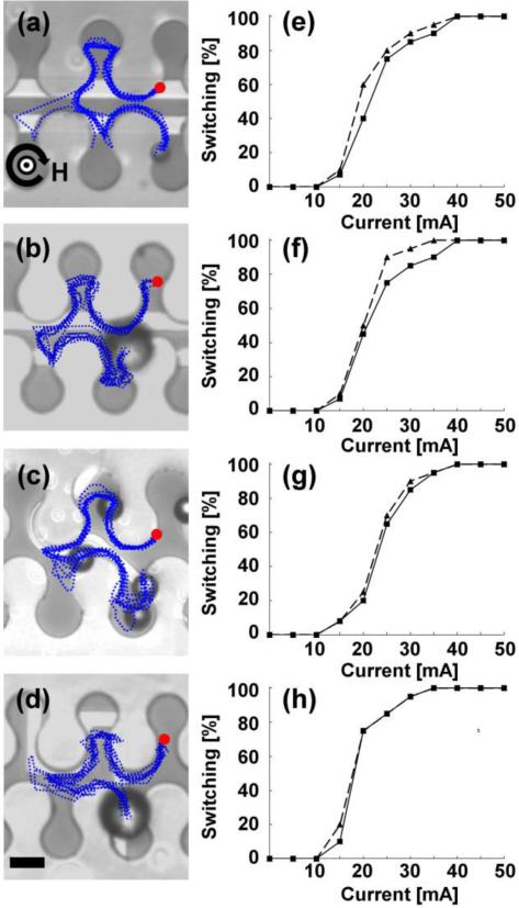
The operating conditions for the transistors illustrated in (a-d) include horizontal and vertical magnetic field components fixed at 50 Oe, while the in-plane field component rotates clockwise at a driving frequency of 0.1 Hz. The gate currents required for reliable switching in each of the transistor geometries are (a) 35 mA, (b) 35 mA, (c) 45 mA, and (d) 40 mA, respectively. The blue dotted lines depict the trajectories of magnetic particles, which are extracted from video data. The red circles depict the starting points of the overlaid trajectories, and the curved black arrow represents the rotation sense of the horizontal field component with the direction of the vertical field depicted at the center of the curved arrow. Four example trajectories are also shown in Supplementary Movies S1-4. The switching thresholds for 8.4 μm beads (solid lines) and 15.6 μm beads (dashed lines) for the transistors depicted in a-d are shown in e-h. Scale bar, 10 μm.
Some representative particle motions are depicted in Figure 3a-d, which presents the overlaid trajectories (blue dotted lines) of ten magnetic beads. For these experiments, the field strength was fixed at 70 Oe, cone angle at 45°, driving frequency of 0.1 Hz, and transistor gate currents of 35 - 45 mA. Switching was achieved by manually turning on the gate current when the particle arrived at the junction. The particle trajectories depicted in Figure 3 and supplementary movies (S1-S4) are consistent regardless of the size of the particle.
To quantify the switching thresholds of the transistors, we monitored the percentage of successful magnetic bead crossings as a function of the applied gate currents. In these experiments, the external field consisting of an in-plane 50 Oe magnetic field rotating at 0.1 Hz that is superimposed with a 50 Oe vertical magnetic field (corresponding to a 45° cone angle). For each transistor, we measured the trajectory of at least twenty magnetic beads in order to obtain statistics on the switching efficiency. The results are illustrated in Fig. 3e-h.
For ease of discussion, we also define a second class of transistors, hereafter denoted as “repulsion transistors”, which are based on straight (or slightly curved) gate currents aligned parallel to the track direction (See Figure 4). Here, the switching mechanism relies on supplying gate currents that produce an in-plane field component, which is anti-parallel to the in-plane component of the external field. The local reduction in field strength causes the particle to be repelled away from the current magnetic track and attracted towards a nearby magnetic track, thus completing the switching process. In some cases, we employ a two-wire geometry, in which anti-parallel currents are used both to repel the bead from one side and attract the bead to the other side of the transistor junction (Fig. 4a-b). Due to closer proximity to the first wire, the repulsion is always stronger than the attraction by the wire that on the opposite side of the junction. One-wire configurations (Fig. 4c-d) could achieve particle switching, but only in the repulsive direction, as the attractive force from the opposite wire was insufficient to significantly alter the local potential energy landscape. Supplementary Movies S5-S8 show example trajectories of beads moving in these repulsion transistors. The switching thresholds of the repulsion transistors are quantified by monitoring the percentage of successful magnetic bead crossings as a function of the applied gate currents (See Fig. 4e-h). The results for all eight transistors, shown in Figures 3 and 4 collectively represent over 3000 individual measurements of the switching efficiency of single beads in different gate currents.
Figure 4. Repulsion transistors.
The horizontal and vertical magnetic field components are fixed at 50 Oe, while the in-plane field component rotates clockwise at a driving frequency of 0.1 Hz. The gate currents required for reliable switching in each of the transistor geometries are (a) 35 mA, (b) 30 mA, (c) 35 mA, and (d) 30 mA, respectively. The blue dotted lines depict the trajectories of magnetic particles, which are extracted from video data. The red circles depict the starting points of the overlaid trajectories, and the curved black arrow represents the rotation sense of the horizontal field component with the direction of the vertical field is depicted at the center of the curved arrow. Four example trajectories are also shown in Supplementary Movies S5-S8. The switching thresholds for 8.4 μm beads (solid lines) and 15.6 μm beads (dashed lines) for the transistors depicted in a-d are shown in e-h. Scale bar, 10 μm.
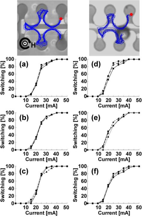
As observed in Figures 3 and 4, the switching thresholds were relatively similar across the different class of transistors. However, based on the tighter spread of the trajectories of the transistors depicted in Figs. 3b and 4b, we selected these for further testing of different experimental conditions.The switching efficiency for the two selected transistors is presented in Figure 5 as a function of the driving frequency (Figs. 5a,d), field strength (Figs. 5b,e), and field cone angle (Figs. 5c,f). For these experiments, in order to more closely simulate our immune cell population of interest, we use only the 8.4-μm diameter magnetic beads, and we present comparative examples in each of the figure panels. Fig. 5a-c shows the results for the barrier transistor depicted in Fig. 3b, while Fig. 5d-f shows similar experiments for the repulsion transistor of Fig. 4b. The switching thresholds only weakly depend on field strengths ranging from 50 – 90 Oe, cone angles ranging from 37° - 65°, and driving frequencies ranging from 0.1 – 0.6 Hz.
Figure 5. Transistor switching thresholds vs. field strength, frequency, and cone angle.
The switching efficiency of 8.4-μm magnetic beads is shown for the transistor depicted in Figure 3b as a function of (a) the driving frequency ranging from 0.1 Hz (solid line), 0.3Hz (dashed line), and 0.6Hz (dotted line) when the field magnitude and cone angle are fixed at 70 Oe and 45°, respectively, (b) the field magnitude ranging from 50 Oe (solid line), 70 Oe (dashed line), and 90 Oe (dotted line) when the cone angle and the driving frequency are fixed at 45° and 0.1Hz, respectively, and (c) the cone angle ranging from degrees 37° (solid line), 45° degrees (dashed line), and 65° degrees (dotted line) when the field magnitude and driving frequency are fixed at 70Oe and 0.1 Hz, respectively. The results from similar experiments performed on the transistor depicted in Figure 4b are shown in (d-f). The red circle depicts the starting points of the overlaid trajectories, and the curved black arrow represents the rotation sense of the horizontal field component with the direction of the vertical field is depicted at the center of the curved arrow.
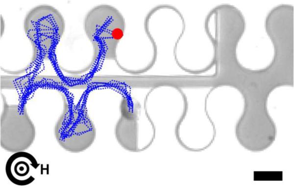
We also demonstrated the ability to switch the trajectory of magnetically labeled CD4+ human T cells with these transistor geometries (Fig. 6). The blue dotted lines present multiple overlaid cell trajectories, which demonstrate the reliability of switching. Supplementary Movies S9-S11 depict the switching trajectories of T cells using different types of transistors.
Figure 6. Transistor switching of magnetically labeled CD4+ T cells.
The overlaid trajectories (blue dotted lines) of magnetically labeled human T cells are shown with the horizontal and vertical magnetic field components fixed at 50 Oe, while the in-plane field component rotates clockwise at a driving frequency of 0.1 Hz. The gate current is fixed at 50 mA. The blue dotted lines depict the trajectories of the cells extracted from video data. The red circle depicts the starting points of the overlaid trajectories, and the curved black arrow represents the rotation sense of the horizontal field component with the direction of the vertical field is depicted at the center of the curved arrow. Examples of switching trajectories are shown in Supplementary Movies S9-S11. Scale bar, 10 μm.
Discussion
Compared to prior work on magnetophoretic circuits in a 2-D in-plane rotating magnetic field, there are fundamental advantages offered by a 3-D conical magnetic field that improves system performance by inducing repulsion between the mobile components. This feature helps not just to inhibit the formation of particle clusters, but also allows these circuits to operates more similarly to electrical circuits, which uses the self-repulsion between the individual electrons to achieve various functions, such as preventing charge accumulation in capacitors. The vertical field bias is also helpful in breaking the mirror symmetry of the rotating field, which allows the stable positions of a particle on a substrate to be uniquely defined, as compared to the degenerate bistable state that is present in a 2-D in-plane rotating field. This effect both improves the synchronization of particle motion relative to the global clock cycle, and it also allows two magnetic tracks to be placed close together without concern about inadvertent switching between the different tracks.
Among the tested transistors, the symmetric geometries (e.g., those in Figs. 3a,b,d, and 4a,b) are preferable because of their bi-directional switching properties. Moreover, transistors with shorter gate electrodes are superior, since they have lower electrical resistance, and hence they require smaller operating voltages. Integrating these transistors into higher-level circuit designs, such as crossbar memory architectures, will require many transistors to be connected in series. Therefore, the reduction of gate electrode resistance is one of the most important parameters for selecting a transistor design.
Finally, the spread of the particle trajectories in the barrier transistors of Figure 3 have tighter overlap compared to the ones shown in Figure 4. Though this is a qualitative measure, it provides an indication of a transistor's repeatability in switching particles between two discrete points in space. For comparison, we provide one example of a switching error in Fig. 4a, in which the magnetic bead was transferred to a different part of the track than intended. Though this type of switching error will often not be problematic, it can interfere with synchronization of downstream logic operations.
Compared to our prior work on transistors designed for 2D in-plane rotating fields, the transistors designed for a 3D conical field require higher gate currents to achieve 100% switching efficiency, which increases the voltage requirements for operating large multiplexed arrays. The increase in the required gate current results, in part, from the vertical field bias, which induces greater energy barriers between the different magnetic tracks. On the other hand, these transistors have a lower propensity for inadvertent switching of particles between distinct tracks, and thus provide motivation for further optimizing the devices to reduce the switching thresholds.
Finally, we find that the switching properties only weakly depend on the particle size, driving frequency, field strength, and the cone angle of the external field. These results indicate that the system is robust and insensitive to the operating conditions, which is an advantage when employing these principles to sort and manipulate biological particles and immune cells whose size, antigen receptor density, and other biological characteristics can vary substantially from one cell population and sub-population to another.
The results presented in this paper thus complete the analogous set of circuit component (conductors, diodes, transistors) required to form hierarchical control architectures enabling the scalable placement of many objects inside microfluidic environments in a 3-D driving field. We envision coupling these circuit elements with microfluidic channels to rapidly organize multicomponent patterns of cells and particles in a high-density array. These cellular arrays can be used in drug screening and to characterize dynamic cellular processes, such as the immunological interactions between pairs of single cells. Ultimately, this manipulation strategy can have an important impact on single cell biology by improving our immunological and molecular understanding of rare and critical single cells.
Supplementary Material
Acknowledgments
The authors are thankful to Hamidreza Toroghi for providing the illustration in Figure 1a. This research was supported by the Creative and Novel Ideas in HIV Research Program (CNIHR) through a supplement to the University of Alabama at Birmingham (UAB) Center For AIDS Research funding (P30 AI027767). This funding was made possible by collaborative efforts of the Office of AIDS Research, the National Institutes of Allergies and Infectious Diseases, and the International AIDS Society. This study was also supported by NIH grant 1R56AI112360, the Duke University CFAR (5P30 AI064518), and Lews Fellowship from the Pratt School of Engineering, Duke University. This work was performed in part at the Duke University Shared Materials Instrumentation Facility (SMIF), a member of the North Carolina Research Triangle Nanotechnology Network (RTNN), which is supported by the National Science Foundation (Grant ECCS-1542015) as part of the National Nanotechnology Coordinated Infrastructure (NNCI).
References
- 1.Wang Y, Navin NE. Molecular Cell. 2015;58(4):598–609. doi: 10.1016/j.molcel.2015.05.005. [DOI] [PMC free article] [PubMed] [Google Scholar]
- 2.Wills QF, Mead AJ. Human Molecular Genetics. 2015;24(R1):R74–R84. doi: 10.1093/hmg/ddv235. [DOI] [PMC free article] [PubMed] [Google Scholar]
- 3.Heath JR, Ribas A, Mischel PS. Nature Reviews Drug Discovery. 2016;15(3):204–216. doi: 10.1038/nrd.2015.16. [DOI] [PMC free article] [PubMed] [Google Scholar]
- 4.Razooky B, Gutierrez E, Terry VH, Spina CA, Groisman A, Weinberger LS. Lab on a Chip. 2012;12(21):4305–4312. doi: 10.1039/c2lc40170c. [DOI] [PMC free article] [PubMed] [Google Scholar]
- 5.Dar RD, Hosmane NN, Arkin MR, Siliciano RF, Weinberger LS. Science. 2014;344(6190):1392–1396. doi: 10.1126/science.1250220. [DOI] [PMC free article] [PubMed] [Google Scholar]
- 6.Han Q, Bagheri N, Bradshaw EM, Hafler DA, Lauffenburger DA, Love JC. Proceedings of the National Academy of Sciences of the United States of America. 2012;109(5):1607–1612. doi: 10.1073/pnas.1117194109. [DOI] [PMC free article] [PubMed] [Google Scholar]
- 7.Fan HC, Fu GK, Fodor SP. Science. 2015;347(6222):1258367. doi: 10.1126/science.1258367. [DOI] [PubMed] [Google Scholar]
- 8.Yamanaka YJ, Szeto GL, Gierahn TM, Forcier TL, Benedict KF, Brefo MSN, Lauffenburger DA, Irvine DJ, Love JC. Analytical Chemistry. 2012;84(24):10531–10536. doi: 10.1021/ac302264q. [DOI] [PMC free article] [PubMed] [Google Scholar]
- 9.Rotem A, Ram O, Shoresh N, Sperling RA, Schnall-Levin M, Zhang H, Basu A, Bernstein BE, Weitz DA. PLoS ONE. 2015;10(5):e0116328. doi: 10.1371/journal.pone.0116328. [DOI] [PMC free article] [PubMed] [Google Scholar]
- 10.Spencer SJ, Tamminen MV, Preheim SP, Guo MT, Briggs AW, Brito IL, Weitz DA, Pitkänen LK, Vigneault F, Juhani Virta MP, Alm EJ. ISME. 2016;10(2):427–436. doi: 10.1038/ismej.2015.124. [DOI] [PMC free article] [PubMed] [Google Scholar]
- 11.Kobel S, Valero A, Latt J, Renaud P, Lutolf M. Lab on a Chip. 2010;10(7):857–863. doi: 10.1039/b918055a. [DOI] [PubMed] [Google Scholar]
- 12.Jin D, Deng B, Li JX, Cai W, Tu L, Chen J, Wu Q, Wang WH. Biomicrofluidics. 2015;9(1):014101. doi: 10.1063/1.4905428. [DOI] [PMC free article] [PubMed] [Google Scholar]
- 13.Kimmerling RJ, Lee Szeto G, Li JW, Genshaft AS, Kazer SW, Payer KR, de Riba Borrajo J, Blainey PC, Irvine DJ, Shalek AK, Manalis SR. Nature Communications. 2016;7:10220. doi: 10.1038/ncomms10220. [DOI] [PMC free article] [PubMed] [Google Scholar]
- 14.Fabbri F, Carloni S, Zoli W, Ulivi P, Gallerani G, Fici P, Chiadini E, Passardi A, Frassineti GL, Ragazzini A, Amadori D. Cancer Letters. 2013;335(1):225–231. doi: 10.1016/j.canlet.2013.02.015. [DOI] [PubMed] [Google Scholar]
- 15.Fritzsch FS, Rosenthal K, Kampert A, Howitz S, Dusny C, Blank LM, Schmid A. Lab on a Chip. 2013;13(3):397–408. doi: 10.1039/c2lc41092c. [DOI] [PubMed] [Google Scholar]
- 16.Mittal N, Rosenthal A, Voldman J. Lab on a Chip. 2007;7(9):1146–1153. doi: 10.1039/b706342c. [DOI] [PubMed] [Google Scholar]
- 17.Peeters DJ, De Laere B, Van den Eynden GG, Van Laere SJ, Rothe F, Ignatiadis M, Sieuwerts AM, Lambrechts D, Rutten A, van Dam PA, Pauwels P, Peeters M, Vermeulen PB, Dirix LY. British Journal of Cancer. 2013;108(6):1358–1367. doi: 10.1038/bjc.2013.92. [DOI] [PMC free article] [PubMed] [Google Scholar]
- 18.Neuman KC, Block SM. The Review of Scientific Instruments. 2004;75(9):2787–2809. doi: 10.1063/1.1785844. [DOI] [PMC free article] [PubMed] [Google Scholar]
- 19.Jing P, Wu J, Liu GW, Keeler EG, Pun SH, Lin LY. Scientific Reports. 2016;6:19924. doi: 10.1038/srep19924. [DOI] [PMC free article] [PubMed] [Google Scholar]
- 20.Collins D, Morahan B, Garcia-Bustos J, Doerig C, Plebanski M, Neild A. Nature Communications. 2015;6:8686. doi: 10.1038/ncomms9686. [DOI] [PMC free article] [PubMed] [Google Scholar]
- 21.Marx V. Nature Methods. 2015;12(1):41–44. doi: 10.1038/nmeth.3218. [DOI] [PubMed] [Google Scholar]
- 22.Abedini-Nassab R, Eslamian M. Recent patents on nanotechnology. 2014;8(3):157–164. doi: 10.2174/1872210508666141022113849. [DOI] [PubMed] [Google Scholar]
- 23.Hejazian M, Li W, Nguyen NT. Lab on a Chip. 2015;15(4):959–970. doi: 10.1039/c4lc01422g. [DOI] [PubMed] [Google Scholar]
- 24.Wang ZM, Wu RG, Wang ZP, Ramanujan RV. Scientific Reports. 2016;6:26945. doi: 10.1038/srep26945. [DOI] [PMC free article] [PubMed] [Google Scholar]
- 25.Romain G, Senyukov V, Rey-Villamizar N, Merouane A, Kelton W, Liadi I, Mahendra A, Charab W, Georgiou G, Roysam B, Lee DA, Varadarajan N. Blood. 2014;124(22):3241–3249. doi: 10.1182/blood-2014-04-569061. [DOI] [PMC free article] [PubMed] [Google Scholar]
- 26.Varadarajan N, Kwon DS, Law KM, Ogunniyi AO, Anahtar MN, Richter JM, Walker BD, Love JC. Proceedings of the National Academy of Sciences of the United States of America. 2012;109(10):3885–3890. doi: 10.1073/pnas.1111205109. [DOI] [PMC free article] [PubMed] [Google Scholar]
- 27.Xue Q, Lu Y, Eisele MR, Sulistijo ES, Khan N, Fan R, Miller-Jensen K. Science Signalling. 2015;8(381):ra59. doi: 10.1126/scisignal.aaa2155. [DOI] [PMC free article] [PubMed] [Google Scholar]
- 28.Abedini-Nassab R, Joh DY, Van Heest MA, Yi J, Baker C, Taherifard Z, Margolis DM, Garcia-Martinez V, Chilkoti A, Murdoch DM, Yellen BB. Advanced Materials. 2015;27(40):6176–6180. doi: 10.1002/adma.201502352. [DOI] [PMC free article] [PubMed] [Google Scholar]
- 29.Lim B, Reddy V, Hu X, Kim K, Jadhav M, Abedini-Nassab R, Noh Y, Lim Y, Yellen BB, Kim C. Nature Communications. 2014;5:3846. doi: 10.1038/ncomms4846. [DOI] [PubMed] [Google Scholar]
- 30.Abedini-Nassab R, Murdoch DM, Kim C, Yellen BB. Journal of Applied Physics. 2014;115(24):244509. [Google Scholar]
- 31.Hejazian M, Nguyen NT. Biomicrofluidics. 2016;10(4):044103. doi: 10.1063/1.4955421. [DOI] [PMC free article] [PubMed] [Google Scholar]
- 32.Yellen BB, Hovorka O, Friedman G. Proceedings of the National Academy of Sciences of the United States of America. 2005;102(25):8860–8864. doi: 10.1073/pnas.0500409102. [DOI] [PMC free article] [PubMed] [Google Scholar]
- 33.Kose AR, Fischer B, Mao L, Koser H. Proceedings of the National Academy of Sciences of the United States of America. 2009;106(51):21478–21483. doi: 10.1073/pnas.0912138106. [DOI] [PMC free article] [PubMed] [Google Scholar]
- 34.Abedini-Nassab R, Joh DY, Triggiano MA, Baker C, Chilkoti A, Murdoch DM, Yellen BB. Advanced Functional Materials. 2016;26(22):4026–4034. doi: 10.1002/adfm.201503898. [DOI] [PMC free article] [PubMed] [Google Scholar]
- 35.Eschenfelder A. Magnetic Bubble Technology. Vol. 14. Springer; Berlin–Heidelberg: p. 1981. [Google Scholar]
- 36.Cohen M, Beall G, Hsieh W, Chang H. IEEE Transactions on Magnetics. 1977;13(5):1264–1266. [Google Scholar]
- 37.Cohen M, Chang H. Proceedings of the IEEE. 1975;63(8):1196–1206. [Google Scholar]
- 38.Tao SL, Popat K, Desai TA. Nature Protocols. 2007;1(6):3153–3158. doi: 10.1038/nprot.2006.451. [DOI] [PubMed] [Google Scholar]
- 39.Hucknall A, Kim D, Rangarajan S, Hill RT, Reichert WM, Chilkoti A. Advanced Materials. 2009;21(19):1968–1971. doi: 10.1002/adma.200803125. [DOI] [PMC free article] [PubMed] [Google Scholar]
Associated Data
This section collects any data citations, data availability statements, or supplementary materials included in this article.


